

UNITRODE UCC1917, UCC2917, UCC3917 Technical data
查询UCC1917供应商
Positive Floating Hot Swap Power Manager
FEATURES
Manages Hot Swap of 15V and
•
Above
Precision Fault Threshold
•
Programmable Average Power
•
Limiting
Programmable Linear Current
•
Control
Programmable Overcurrent Limit
•
Programmable Fault Time
•
Internal Charge Pump to Control
•
External NMOS Device
Fault Output and Catastrophic
•
Fault Indication
• Fault Mode Programmable to
Latch or Retry
• Shutdown Control
• Undervoltage Lockout
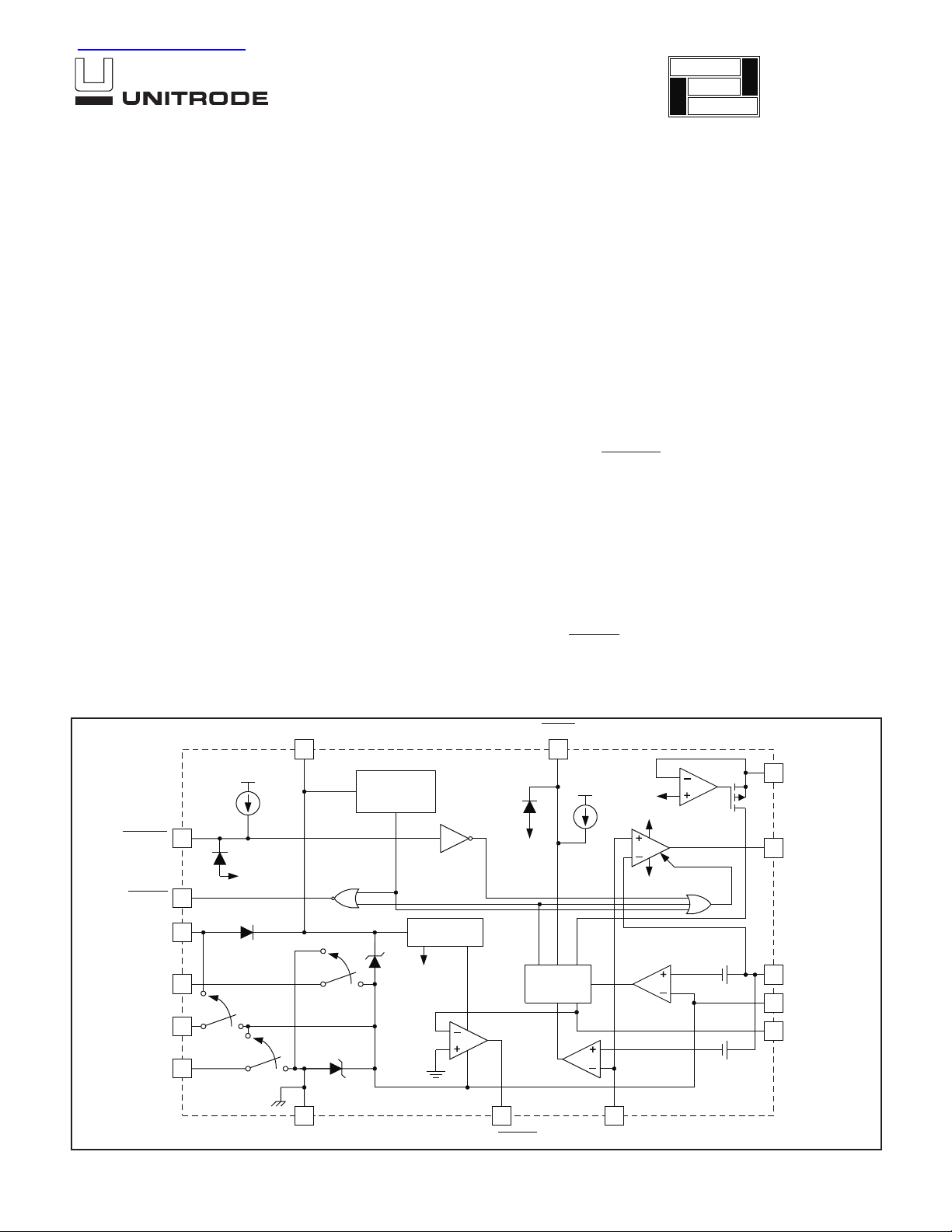
BLOCK DIAGRAM
V
DD
40µA
SHTDWN
12
DESCRIPTION
The UCC3917 family of positive floating hot swap managers provides complete
power management, hot swap, and fault handling capability. The voltage limita
tion of the application is only restricted by the external component voltage limi
tations. The IC provides its own supply voltage via a charge pump off of VOUT.
The onboard 10V shunt regulator protects the IC from excess voltage. The IC
also has catastrophic fault indication to alert the user that the ability to shut off
the output NMOS has been bypassed. All control and housekeeping functions
are integrated and externally programmable. These include the fault current
level, maximum output sourcing current, maximum fault time, soft start time,
and average NMOS power limiting.
The fault level across the current sense amplifier is fixed at 50mV to minimize
total drop out. Once 50mV is exceeded across the current sense resistor, the
fault timer will start. The maximum allowable sourcing current is programmed
with a voltage divider from the VREF/CATFLT
on the MAXI pin. The current level at which the output appears as a current
source is equal to V
trolled current startup can be programmed with a capacitor on MAXI.
When the output current is below the fault level, the output device is switched
on with full gate drive. When the output current exceeds the fault level, but is
less than maximum allowable sourcing level programmed by MAXI, the output
remains switched on, and the fault timer starts charging CT. Once CT charges
to 2.5V, the output device is turned off and attempts either a retry sometime
later or waits for the state on the LATCH
the output current reaches the maximum sourcing current level, the output device appears as a current source.
13 16
UVLO
>10V=ENABLE
< 6V=DISABLE
MAXI divided by the current sense resistor. If desired, a con
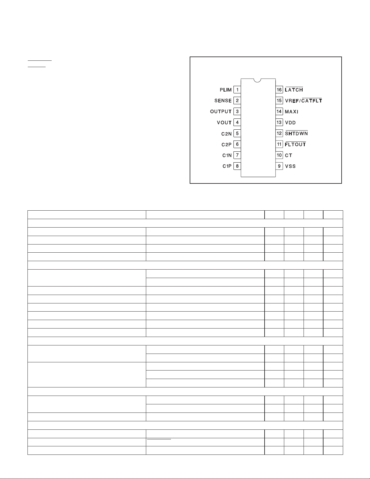
LATCHVDD
V
DD
VOUT
application
INFO
available
UCC1917
UCC2917
UCC3917
pin to generate a fixed voltage
pin to change if in latch mode. When
1
PLIM
5V
VDD
40µA
DISABLE
3
OUTPUT
-
-
-
VOUT
FLTOUT
C1P
C1N
C2P
C2N
11
8
7
6
5
SLUS203A - AUGUST 1999
5V
REFERENCE
LOGIC
SUPPLY
4V
9 15 14
VSS VREF/CATFLT MAXI
ON-TIME
DELAY
VOUT
OVER
CURRENT
COMPARATOR
OUTPUT
LOW
200mV
50mV
+
+
10
2
4
SENSE
VOUT
CT
UDG-99055
ABSOLUTE MAXIMUM RATINGS
IDD . . . . . . . . . . . . . . . . . . . . . . . . . . . . . . . . . . . . . . . . . . 20mA
SHTDWN
LATCH
VREF Current . . . . . . . . . . . . . . . . . . . . . . . . . . . . . . . . –500µA
PLIM Current . . . . . . . . . . . . . . . . . . . . . . . . . . . . . . . . . . 10mA
MAXI Input Voltage . . . . . . . . . . . . . . . . . . . . . . . . . VDD + 0.3V
Storage Temperature . . . . . . . . . . . . . . . . . . . –65°C to +150°C
Junction Temperature. . . . . . . . . . . . . . . . . . . –55°C to +150°C
Lead Temperature (Soldering, 10 sec.) . . . . . . . . . . . . . +300°C
Currents are positive into, negative out of the specified
terminal. Consult Packaging Section of Databook for thermal
limitations and considerations of package.
Current . . . . . . . . . . . . . . . . . . . . . . . . . . . . . –500µA
Current . . . . . . . . . . . . . . . . . . . . . . . . . . . . . . . –500µA
UCC1917
UCC2917
UCC3917
CONNECTION DIAGRAM
DIL-16, SOIC-16 (Top View)
J or N Package, D Package
ELECTRICAL CHARACTERISTICS:
UCC2917 and –55°C to 125°C for the UCC1917, C
Unless otherwise specified, TA= 0°C to 70°C for the UCC3917, –40°C to 85° for the
= 4.7nF. TA=TJ. All voltages are with respect to VOUT. Current is positive
T
into and negative out of the specified terminal.
PARAMETER TEST CONDITIONS MIN TYP MAX UNITS
VDD Section
I
DD From VOUT (Note 1) 3.0 5 11 mA
UVLO Turn On Threshold 7.9 8.8 9.7 V
UVLO Off Voltage 5.5 6.5 7.5 V
VSS Regulator Voltage –6 –5 –4 V
Fault Timing Section
Overcurrent Threshold T
A = 25°C 47.5 50 53 mV
Over Operating Temperature 46 50 54 mV
Overcurrent Input Bias 50 500 nA
CT Charge Current V
CT = 1V –78 –50 –28 µA
CT Catastrophic Fault Threshold 3.4 4.5 V
CT Fault Threshold 2.25 2.5 2.75 V
CT Reset Threshold 0.32 0.5 0.62 V
Output Duty Cycle Fault Condition 1.7 2.7 3.7 %
Output Section
Output High Voltage I
Output Low Voltage I
OUT = 0 6 8 10 V
OUT = –500µA 579V
I
OUT = 0 0 0.05 V
OUT = 500µA 0.1 0.5 V
I
OUT = 1mA 0.5 0.9 V
I
Linear Current Section
Sense Control Votlage MAXI = 100mV 85 100 115 mV
MAXI = 400mV 370 400 430 mV
Input Bias MAXI = 200mV 50 500 nA
SHUTDOWN Section
Shutdown Threshold 2.0 2.4 2.8 V
Input Current SHTDWN
= 0V 24 40 60 µA
Shutdown Delay 100 500 ns
2
UCC1917
UCC2917
UCC3917
ELECTRICAL CHARACTERISTICS:
the UCC2917 and –55°C to 125°C for the UCC1917, C
positive into and negative out of the specified terminal.
PARAMETER TEST CONDITIONS MIN TYP MAX UNITS
LATCH Section
Latch Threshold 1.7 2 2.3 V
Input Current LATCH = 0V 24 40 60 µA
Fault Out Section
Fault Output High 6 8 10 V
Fault Output Low 0.01 0.05 V
Power Limiting Section
SENSE Regulator Voltage I
V
Duty Cycle Control I
VREF/CATFLT Section
V
REF Regulator Voltage 4.5 5 5.5 V
Fault Output Low I
Output Sink Current V
Overload Comparator Threshold Relative to MAXI 110 200 290 mV
Note 1: Set by user with RSS.
Unless otherwise specified, TA= 0°C to 70°C for the UCC3917, –40°C to 85° for
= 4.7nF. TA=TJ. All voltages are with respect to VOUT. Current is
T
= 64µA 4.5 5 5.5 V
PLIMIT
= 64µA 0.6 1.2 1.7 %
PLIMIT
= 1mA 0.045 0.1 0.2 %
I
PLIMIT
VREF/CATFLT
=
CT
= 5mA 0.22 0.50 V
5V, V
VREF/CATFLT
= 5V 15 40 70 mA
PIN DESCRIPTIONS
C1N: Negative side of the upper charge pump capacitor.
C1P: Positive side of the upper charge pump capacitor.
C2N: Negative side of the lower charge pump capacitor.
C2P: Positive side of lower charge pump capacitor.
CT: A capacitor is connected to this pin to set the fault
time. The fault time must be more than the time to
charge the external load capacitance (see Application In
formation).
FLTOUT
: This pin provides fault output indication. Inter
face to this pin is usually performed through level shift
transistors. Under a non-fault condition, FLTOUT
will pull
to a high state. When a fault is detected by the fault timer
or the under voltage lockout, this pin will drive to a low
state, indicating the output NMOS is in the off state.
LATCH
: Pulling this pin low causes a fault to latch until
this pin is brought high or a power on reset is attempted.
However, pulling this pin high before the reset time is
reached will not clear the fault until the reset time is
reached. Keeping LATCH
high will result in normal oper
ation of the fault timer. Users should note there will be an
RC delay dependent upon the external capacitor at this
pin.
MAXI: This pin programs the maximum allowable sour
cing current. Since VREF/CATFLT
is a regulated volt
age, a voltage divider can be derived to generate the
program level for MAXI. The current level at which the
output appears as a current source is equal to the volt
age on MAXI divided by the current sense resistor. If desired, a controlled current start up can be programmed
with a capacitor on MAXI (to VOUT), and a programmed
start delay can be achieved by driving the shutdown with
an open collector/drain device into an RC network.
OUTPUT: Gate drive to the NMOS pass element.
PLIM: This feature ensures that the average external
-
NMOS power dissipation is controlled. A resistor is con
nected from this pin to the drain of the external NMOS
pass element. When the voltage across the NMOS ex
ceeds 5V, current will flow into PLIM which adds to the
fault timer charge current, reducing the duty cycle from
the 3% level.
SENSE: Input voltage from the current sense resistor.
When there is greater than 50mV across this pin with re
spect to VOUT, a fault is sensed, and CT starts to
charge.
SHTDWN
: This pin provides shutdown control. Interface
to this pin is usually performed through level shift transis
-
tors. When shutdown is driven low, the output disables
the NMOS pass device.
VDD: Power to the I.C. Is supplied by an external current
limiting resistor on initial power-up or if the load is
-
shorted. As the load voltages rises (VOUT), a small
-
amount of power is drawn from VOUT by an internal
charge pump. The charge pump’s input voltage is regu
lated by an on-chip 5V zener. Power to VDD is supplied
-
-
-
-
-
-
3
 Loading...