

查询C1888CT供应商
Off-line Power Supply Controller
UCC1888
UCC2888
UCC3888
FEATURES
•
Transformerless Off-line
Power Supply
•
Wide 100VDC to 400VDC
Allowable Input Range
•
Fixed 5VDC or Adjustable
Low Voltage Output
•
Output Sinks 200mA, Sources
150mA Into a MOSFET Gate
•
Uses Low Cost SMD Inductors
•
Short Circuit Protected
•
Optional Isolation Capability
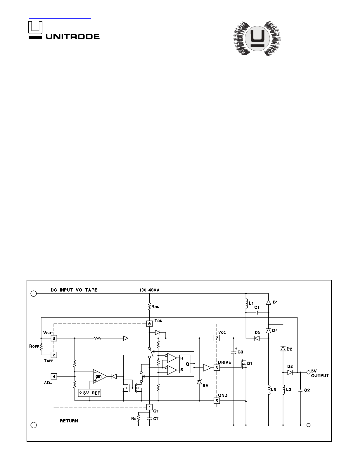
TYPICAL APPLICATION
DESCRIPTION
The UCC3888 controller is optimized for use as an off-line, low power, low voltage,
regulated bias supply. The unique circuit topology utilized in this device can be
visualized as two cascaded flyback converters, each operating in the discontinuous mode, both driven from a single external power switch. The significant benefit
of this approach is the ability to achieve voltage conversion ratios as high as 400V
to 2.7V with no transformer and low internal losses.
The control algorithm utilized by the UCC3888 sets the switch on time inversely
proportional to the input line voltage and sets the switch off time inversely proportional to the output voltage. This action is automatically controlled by an internal
feedback loop and reference. The cascaded configuration allows a voltage conversion from 400V to 2.7V to be achieved with a switch duty cycle of 7.6%. This topology also offers inherent short circuit protection since as the output voltage falls to
zero, the switch off time approaches infin ity.
The output voltage is set internally to 5V. It can be programmed for other output
voltages with two external resis tors. An isolated version can be achieved with this
topology as described fu rth er in Un itrode App licat ion N ote U-1 49.
OPERATION
With reference to the application diagram below, when input voltage is fir st ap plied,
the current through R
capacitor, C3, connected to V
tage lockout holds the circuit off and the output at DRIVE low until V
8.4V. At this time, DRIVE goes high turning on the power switch, Q1, and redirecting the current into T
with a current I
long as C
voltage. This provides a constant (line voltage) • (switch on time) product.
CHG
charges, the power switch on time will be inversely proportional to line
T
into TON is directed to VCC where it charges the external
ON
. As voltage builds on VCC, an internal undervol-
CC
reaches
CC
to the timing capacitor, CT. CT charges to a fixed threshold
ON
=0.8 • (VIN - 4.5V)/RON. Since DRIVE will only be high for as
Note: This devi ce inc orp ora tes patented tec hn ol og y us ed und er license from Lambda Electronics, Inc.
3/97
UDG-96013
OPERATION (cont.)
At the end of the on time, Q1 is turned off and the current
through R
through R
tributes to supplying power to the chip during the off time.
The power sw itch off time is controlle d by the dis charge
of C
which, in turn, is programmed by the regulated out-
T
put voltag e. The relationship between C
rent, I
DCHG
is again diverted to VCC. Thus the current
ON
, which charges CT during the on time, c on-
ON
discharge cur-
T
, and output voltage is illustrated as follows:
UCC1888
UCC2888
UCC3888
I
As V
increases, I
OUT
DCHG
= (V
The operating frequency increases and V
quickly to its regulated value.
Region 3. In th i s r eg i on , a tr ans conductance ampl ifi er re-
duces I
V
Region 4. If V
I
DCHG
DCHG
.
OUT
should rise abov e it s regu lat ion range,
OUT
falls to zero and the circuit returns to
the minimum frequency established by R
C
.
T
The range of switching frequencies is established by
RON, R
, RS, and CT as follows:
OFF
- 0.7V) / R
OUT
increases r e duc ing off time.
DCHG
OFF
rises
OUT
in order to maintain a regulated
and
S
Region 1. When V
feature provides inherent short circuit protection. However, to ensure output voltage
startup when the output is n ot a short, a high
value resistor, R
to establish a minimum switching frequency.
Region 2. As V
OUT
regulated value, I
and is equal to:
= 0, the off time is infinite. This
OUT
, is placed in parallel with C
S
rises above approxi mately 0.7V to its
is defined by R
DCHG
OFF
Frequency = 1/(T
•
T
= R
ON
T
(max) = 1.4 • RS • CT
OFF
ON
C
Regions 1 and 4
T
OFF
= R
OFF
•
Region 2, excluding the effects of R
which have a minimal impact on T
T
The above equations assume that V
voltage at T
6.5V while C
,
increases from approximately 2.5V to
ON
is charging. To take this into account, V
T
is adjusted by 4.5V in the calculation of TON. The voltage
at T
is approximately 0.7V.
OFF
ON
•
4.6
T
C
• 3.7V /(V
T
+ T
)
OFF
V/(VIN - 4.5V)
OUT
CC
- 0.7V)
S
.
OFF
equals 9V. The
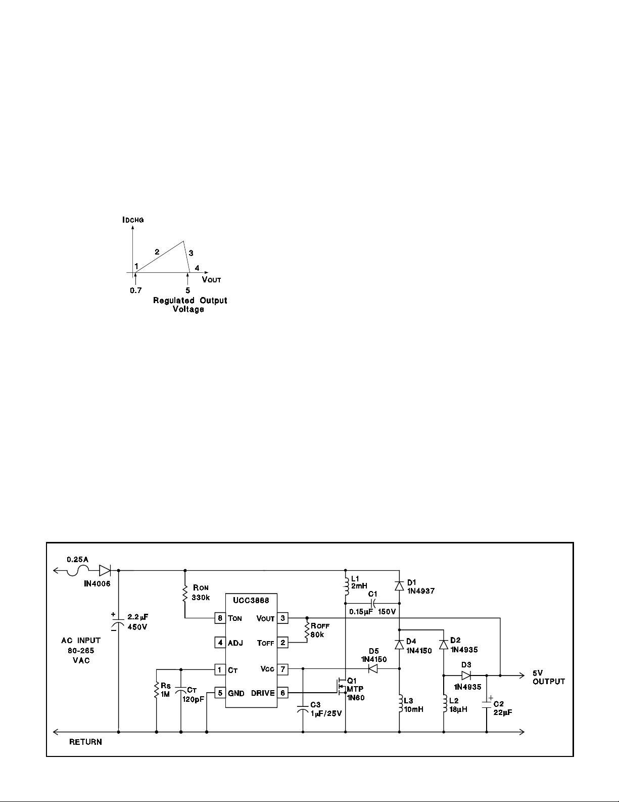
DESIGN EXAMPLE
The UCC3888 regulate s a 5 volt , 1 Watt nonisolated DC output from AC inputs between 80 and 265 volts. In this example, the I C is prog rammed t o deliver a maximum on time gate dri ve pulse width of 2.2 microseconds which occurs
at 80 VAC. The corresponding switching frequency is approximately 100kHz at low line, and overall efficiency is approximately 50%. Additional design information is available in Unitrode Application Note U-149.
IN
UDG-96014
2
 Loading...