

UNITRODE UCC1884, UCC2884, UCC3884 Technical data
查询UCC1884供应商
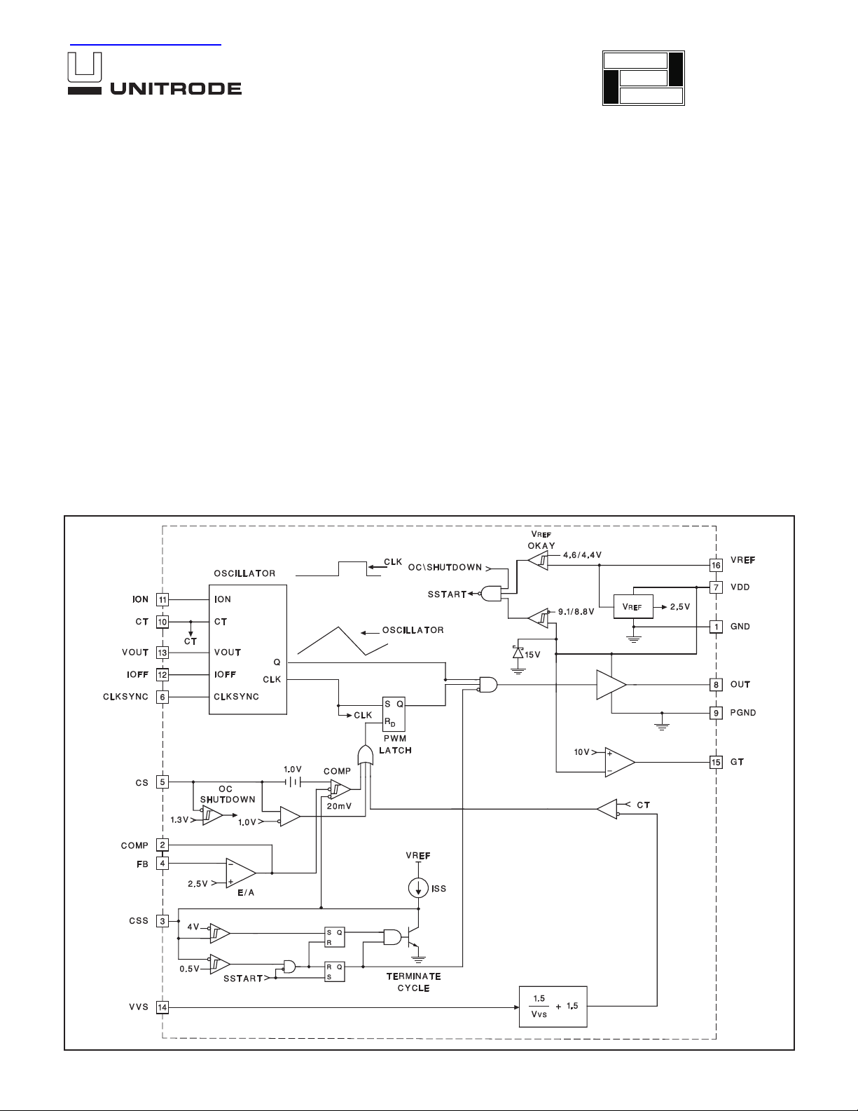
application
Frequency Foldback Current Mode PWM Controller
FEATURES
Frequency Foldback Reduces
•
Operating Frequency Under Fault
Conditions
Accurate Programmable Volt-Second
•
Clamp
Programmable Maximum Duty Cycle
•
Clamp
Oscillator Synchronization
•
Overcurrent Protection
•
Shutdown with Full Soft Start
•
Wide Gain Bandwidth Amplifier
•
(GBW > 2.5MHz)
Current Mode Operation
•
DESCRIPTION
The UCC3884 is a high performance current mode PWM controller in
tended for single ended switch mode power supplies. The chip implements
a frequency foldback scheme that decreases the oscillator frequency as
the output voltage falls below a programmed value. This technique de
creases the average output current sourced into a low impedance load
which can occur during an output short circuit or overload condition. Ex
cessive short circuit current is more prevalent in high frequency converters
where the propagation delay and switch turn-off time forces a minimum at
tainable duty cycle. An accurate volt-second clamp limits the duty cycle
during line or load transient conditions which could otherwise saturate the
transformer. The volt-second clamp may also be used with an external
overvoltage protection circuit to handle fault conditions such as current
sense disconnect or current transformer saturation. The frequency
foldback, volt-second clamp, cycle-by-cycle current limit, and overcurrent
shutdown provide a rich set of protection features for use in peak current
mode pulse width modulators.
INFO
available
UCC1884
UCC2884
UCC3884
PRELIMINARY
-
-
-
-
• Precision 5V Reference
BLOCK DIAGRAM
SLUS160A - AUGUST 1999
UDG-96026-1
ABSOLUTE MAXIMUM RATINGS
Supply Voltage . . . . . . . . . . . . . . . . . . . . . . . . . . . . . . . . . . 15V
Output Sink Current. . . . . . . . . . . . . . . . . . . . . . . . . . . . . . . . 1A
Output Source Current . . . . . . . . . . . . . . . . . . . . . . . . . . . . 0.5A
All Other Pins. . . . . . . . . . . . . . . . . . . . . . . . . . . . . . . . . . . . . 6V
Storage Temperature . . . . . . . . . . . . . . . . . . . –65°C to +150°C
Junction Temperature. . . . . . . . . . . . . . . . . . . –55°C to +150°C
Lead Temperature (Soldering, 10 sec.). . . . . . . . . . . . . +300°C
Currents are positive into, negative out of the specified termi
nal. Consult Packaging Section of Databook for thermal limita
tions and considerations of packages.
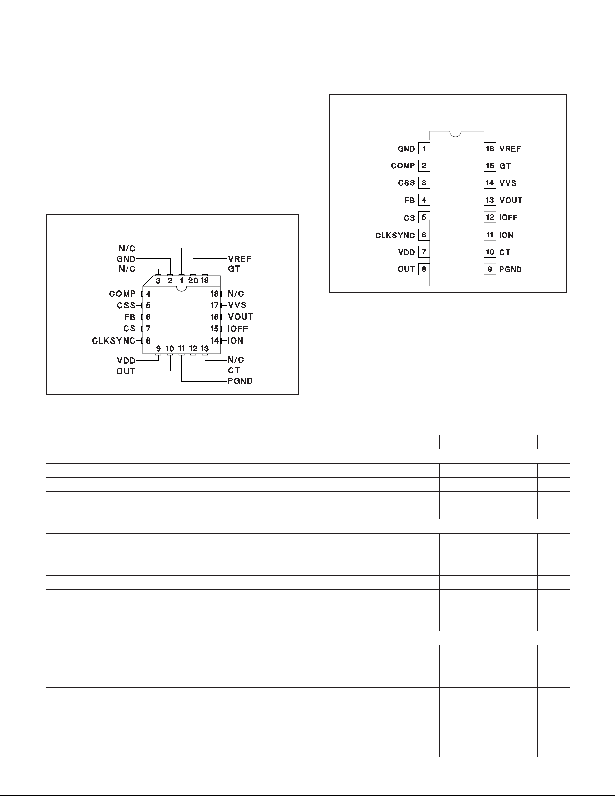
PLCC-20 (Top View)
Q Package
UCC1884
UCC2884
UCC3884
CONNECTION DIAGRAMS
DIL-16, SOIC-16 (Top View)
J, N or D Packages
-
-
ELECTRICAL CHARACTERISTICS: Unless otherwise specified, these specifications apply for TA = –55°C to 125°C for the
UCC1884, –40°C to 85°C for the UCC2884, and 0°C to 70°C for the UCC3884, CT = 220pF, RON= 53k, R
VREF, VVS = 0V, CSS = 2.5nF, VDD = 11V, Output no load, TA=TJ.
PARAMETER TEST CONDITIONS MIN TYP MAX UNITS
5V Reference Section
VREF I
= 0mA 4.86 5 5.14 V
REF
Line Regulation VDD = 10V to 12V 1 10 mV
Load Regulation 0 < I
< 5mA 1 20 mV
REF
Short Circuit I VREF = 0V 15 45 mA
Oscillator Section
Accuracy V
OUT=VREF
360 400 440 kHz
Foldback Frequency VOUT = 0.75V 200 230 260 kHz
CLKSYNC Output High 4.8 5 5.2 V
CLKSYNC Output Low 0.0 0.4 V
CLKSYNC Sink Current CLKSYNC = 1V 1.2 2.2 mA
CLKSYNC Source Current CLKSYNC = 3V –0.2 –0.1 mA
CLKSYNC Input Threshold CLKSYNC from 5V to 0V (Edge Detect) 2.5 3.0 3.5 V
Error Amplifier Section
I
B
Total Bias Current; Regulating Level –1 1 µA
FB Voltage FB = COMP 2.43 2.5 2.57 V
VO 50 90 dB
A
GBW F = 100kHz (Note 1) 2.5 5 MHz
Output Source Current FB = 2.3V, COMP = 2.5V –0.6 –1.2 mA
Output Sink Current FB = 2.7V, V
V
OL
V
OH
IO= 100µA 0.3 0.9 V
IO= –100µA 2.7 3.1 3.5 V
= 1V 0.250 1.5 mA
COMP
= 38k, VOUT =
OFF
2
UCC1884
UCC2884
UCC3884
ELECTRICAL CHARACTERISTICS: Unless otherwise specified, these specifications apply for TA = –55°C to 125°C for the
UCC1884, –40°C to 85°C for the UCC2884, and 0°C to 70°C for the UCC3884, CT = 220pF, RON= 53k, R
VREF, VVS = 0V, CSS = 2.5nF, VDD = 11V, Output no load, TA=TJ.
PARAMETER TEST CONDITIONS MIN TYP MAX UNITS
PWM Section
Minimum Duty Cycle FB = 3V, CS = 0V 0 %
Maximum Duty Cycle FB = 0V, CS = 0V 75 78 81 %
Current Sense Section
Input Bias Current (CS) 3.0 µA
CS Shutdown Threshold 1.235 1.3 1.365 V
CS Shutdown Hysteresis 20 mV
CS Over Current Threshold 0.95 1 1.05 V
Current/Fault Section
Soft Start Charge Current –10 –20 –30 µA
Soft Start Discharge Current 10 20 30 µA
V
OL
Soft Start Complete Threshold 3.6 4 4.4 V
Soft Start Restart Threshold 0.4 0.5 0.6 V
Volt Second Clamp
Duty Cycle VVS = 1.4V, T
VVS = 3.6V, T
VVS = 3.6V, T
VVS = 3.6V, T
I
B
VVS = 3.7V –1 +1 µA
= 0°C to 70°C 53.8 56.8 59.8 %
A
= –55°C to 125°C 19.8 22 26.0 %
A
= –40°C to 85°C 20.9 22 25.0 %
A
= 0°C to 70°C 21 22 23 %
A
Output Stage
Output Low Saturation I
Output High Saturation I
UVLO Output Low Saturation I
= 100mA 0.5 0.9 V
OUT
= –50mA 0.5 0.9 V
OUT
= –200mA (Note 1) 1.9 V
I
OUT
= 20mA, VDD = 0V 0.7 1.2 V
OUT
Rise Time CL = 1nF 50 70 ns
Fall Time CL = 1nF 30 50 ns
Undervoltage Lockout
Turn-On Threshold Voltage 8.4 8.9 9.4 V
Hysteresis 200 600 1000 mV
Startup Regulator
Regulated VDD Voltage 9.5 10 10.5 V
VDD Override Threshold 10.7 V
Overall
Range 14.5 V
V
DD
(run) f = 400kHz 2 5 10 mA
I
DD
I
Startup Current VDD = 5.4V 100 250 µA
DD
VDD Clamp IDD = 10mA 12 13.5 15 V
= 38k, VOUT =
OFF
050mV
Note 1: Guaranteed by design. Not 100% tested in production.
3
 Loading...