

UNITRODE UCC1858, UCC2858, UCC3858 Technical data
查询UCC1858供应商
High Efficiency, High Power Factor Preregulator
UCC1858
UCC2858
UCC3858
PRELIMINARY
FEATURES
• Programmable PWM Frequency
Foldback for Higher Efficiency at Light
Loads
• Leading Edge PWM for Reduced
Output Capacitor Ripple Current
• Controls Boost PWM to Near Unity
Power Factor
• World Wide Operation without
Switches
• Accurate Power Limiting
• Synchronizable Oscillator
• 100µA Startup Supply Current
• Low Power BCDMOS
• 12V to 18V Operation
DESCRIPTION
The UCC3858 provides all of the control functions necessary for active
power factor corrected preregulators which require high efficiency at low
power operation. The controller achieves near unity power factor by
shaping the AC input line current waveform to correspond to the AC input
line voltage using average current mode control.
The operation of the UCC3858 closely resembles that of previously designed Unitrode PFC parts with additional features to allow higher efficiency boost converter operation at light loads. This is accomplished by
linearly scaling back the PWM frequency when the output of the voltage
error amplifier drops below a predetermined user programmable level indicating a light load condition. The frequency is scaled back by reducing
the charging current for the CT ramp (in proportion to the output power),
and increasing the dead time. There is also an instantaneous reset input
to pull the IC out of foldback mode quickly when the load comes back up.
The PWM technique used in the UCC3858 is leading edge modulation.
When combined with the more conventional trailing edge modulation on
the downstream converter, this scheme offers the benefit of reduced ripple current on the bulk storage capacitor. The oscillator is designed for
easy synchronization to the downstream converter. A simple synchronization scheme can be implemented by connecting the PWM output of
the downstream converter to the SYNC pin.
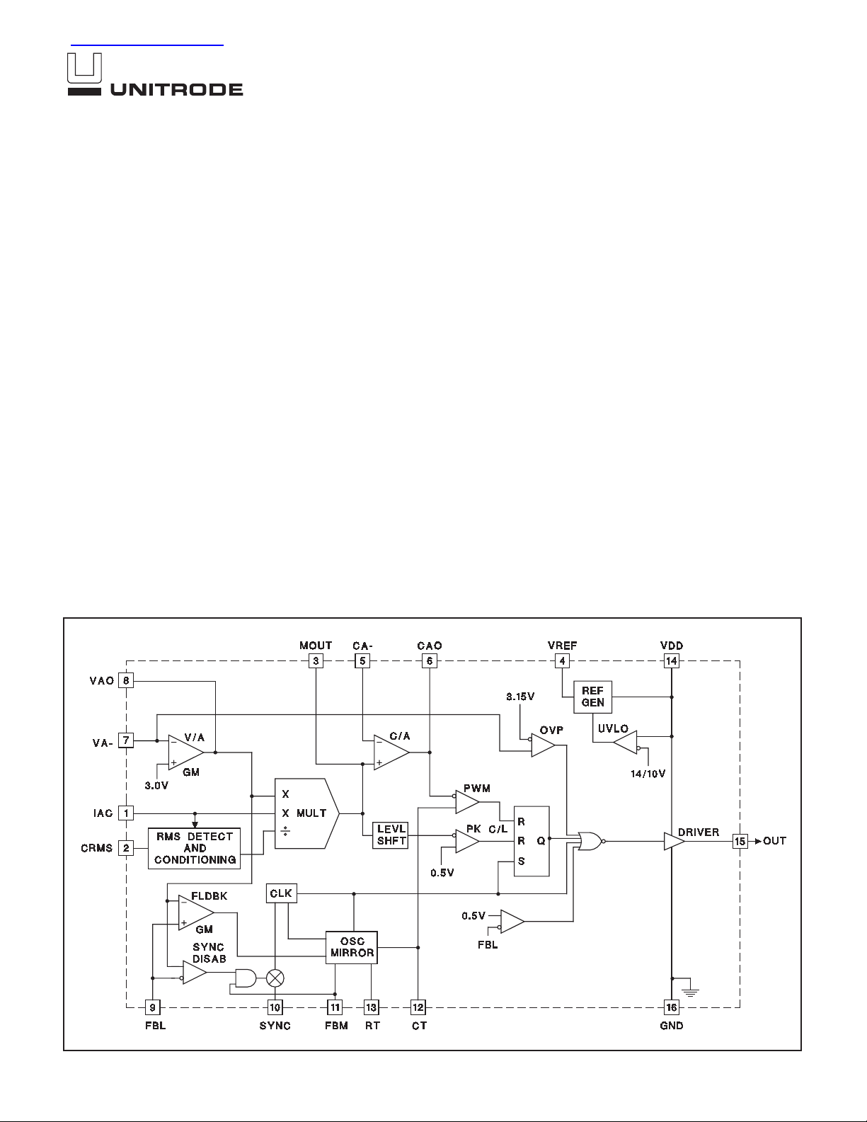
BLOCK DIAGRAM
(continued)
03/99
UDG-96191-1
ABSOLUTE MAXIMUM RATINGS
Supply Voltage VDD. . . . . . . . . . . . . . . . . . . . . . . . . . . . . . 18V
Gate Drive Current
Continuous . . . . . . . . . . . . . . . . . . . . . . . . . . . . . . . . . . 0.2A
Pulsed . . . . . . . . . . . . . . . . . . . . . . . . . . . . . . . . . . . . 500mA
Input Current IAC . . . . . . . . . . . . . . . . . . . . . . . . . . . . . . 200mA
Power Dissipation. . . . . . . . . . . . . . . . . . . . . . . . . . . . . . . . . 1W
Storage Temperature . . . . . . . . . . . . . . . . . . . −65°C to +150°C
Junction Temperature. . . . . . . . . . . . . . . . . . . −55°C to +150°C
Lead Temperature (Soldering, 10 Sec.). . . . . . . . . . . . . +300°C
Analog Inputs
Maximum Forced Voltage . . . . . . . . . . . . . . . . –0.3V to 11V
Unless otherwise indicated, voltages are reference to ground and currents are positive into, negative out of the specified terminal. Pulsed is
defined as a less than 10% duty cycle with a maximum duration of
500ns. Consult Packaging Section of Databook for thermal limitations
and considerations of packages.
DESCRIPTION (cont.)
Controller improvements include an onboard peak detector for the input line RMS voltage, an integrated
overcurrent shutdown, overvoltage shutdown and significantly lower quiescent operating current. The peak detector eliminates an external 2-pole low pass filter for
RMS detection. This simplifies the converter design as
well as providing an approximate 6X improvement in input line transient response. The current signal is extracted from the current error amplifier input to provide a
cycle-by-cycle peak current limit. Low startup and operating currents which are achieved through the use of
UCC1858
UCC2858
UCC3858
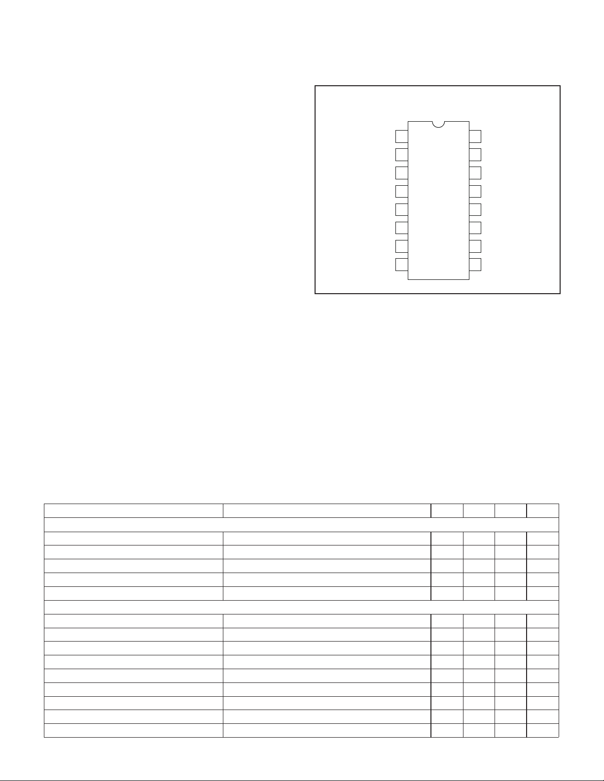
CONNECTION DIAGRAM
DIP-16, SOIC-16 (TOP VIEW)
J, N,DW Packages
IAC
1
VREF
CA–
CAO
VA–
VAO
2
3
4
5
6
7
8
CRMS
MOUT
Unitrode’s BCDMOS process simplify the bootstrap
supply design as well as minimize losses in the control
circuit. A transconductance voltage error amplifier allows
output voltage sensing for internal overvoltage protection.
Additional features include: undervoltage lockout for reliable off-line startup, a precision 7.5V reference, and a
precision RMS detection and signal conditioning circuit.
Chip shutdown can be attained by bringing the FBL pin
below 0.5V.
16
GND
15
OUT
14
VDD
13
RT
12
CT
11
FBM
10
SYNC
9
FBL
ELECTRICAL CHARACTERISTICS:
UCC3858, –40°C to +85°C for the UCC2858, and –55°C to +150°C for the UCC1858, V
96k, I
= 100µA, TA= TJ.
IAC
Unless otherwise stated, these specifications apply for TA= 0°C to 70°C for the
= 12V, RT= 24k, CT= 330pF, R
VDD
PARAMETER TEST CONDITIONS MIN TYP MAX UNITS
Overall
Supply Current, Off V
CAO
, V
= 0V, VDD= UVLO – 0.3V 100 250 µA
VAO
Supply Current, On FBL = 0V 2 3.5 5 mA
VDD Turn-On Threshold 12 13.5 15.5 V
VDD Turn-Off Threshold 10 V
UVLO Hysteresis 3.2 3.5 3.8 V
Voltage Amplifier
Input Voltage T
= 25°C 2.95 3 3.05 V
A
Over Voltage Protection Volts Above VA– Input Voltage 0.12 0.14 0.16 V
VA– Bias Current –0.5 –1 µA
Open Loop Gain V
= 2V to 5V 45 50 dB
OUT
VAO High Load = –25µA 5.7 6 6.3 V
VAO Low Load = 25µA 0.3 0.5 V
Output Source Current V
Output Sink Current V
Transconductance I
– = 2.8V –50 µA
VA
– = 3.2V 50 µA
VA
= ± 50µA 400 600 1000 µS
OUT
2
FBM
=

UCC1858
UCC2858
UCC3858
ELECTRICAL CHARACTERISTICS:
UCC3858, –40°C to +85°C for the UCC2858, and –55°C to +150°C for the UCC1858, V
96k, I
= 100µA, TA= TJ.
IAC
Unless otherwise stated, these specifications apply for TA= 0°C to 70°C for the
= 12V, RT= 24k, CT= 330pF, R
VDD
PARAMETER TEST CONDITIONS MIN TYP MAX UNITS
Current Amplifier
Input Offset Voltage V
Input Bias Current V
Input Offset Current V
Open Loop Gain V
CMRR V
CAO High V
CAO Low V
= 0V, V
CM
= 0V, V
CM
= 0V, V
CM
= 0V, V
CM
= 0V to 1.5V, V
CM
= 0V, V
–
CA
= 1V, V
–
CA
= 3V –3 0 3 mV
CAO
= 3V –6.5 –5 µA
CAO
= 3V –0.5 0.0 0.5 µA
CAO
= 2V to 5V 80 90 dB
CAO
= 3V 65 80 dB
CAO
= 1V, IL= –50µA 6.5 7 7.5 V
MOUT
= 0V, IL= 1mA 0.2 0.3 V
MOUT
Maximum Output Source Current –130 –150 µA
Voltage Reference
Output Voltage I
= 0mA, TA= 25°C 7.313 7.5 7.688 V
REF
Over Temperature, UCC3858 7.294 7.5 7.707 V
Over Temperature, UCC2858, UCC1858 7.239 7.5 7.762 V
Load Regulation I
Line Regulation V
Short Circuit Current V
= 0mA to 2mA 3 5 mV
REF
= 12V to 16V 30 mV
DD
= 0V 35 50 mA
REF
Oscillator
Initial Accuracy TA= 25°C 90 100 110 kHz
Voltage Stability V
= 12V to 16V 1 %
DD
Total Variation Line, Temperature 80 120 kHz
Ramp Amplitude (p-p) Oscillator Free Running, VAO = 5.5V 3.3 3.5 3.7 V
Ramp Peak Voltage Oscillator Free Running, VAO = 5.5V 4.4 4.6 4.8 V
Peak Current Limit
PKLMT Threshold Voltage (V
CA
–)–V
MOUT
350 450 550 mV
PKLMT Hysteresis 100 200 mV
PKLMT Propagation Delay 1 µs
Multiplier Section
High Line, Low Power I
High Line, High Power I
Low Line, Low Power I
Low Line, High Power I
IAC Limited I
Gain Constant I
Zero Current I
Power Limit (V
• IMO)I
CRMS
= 100µA, V
AC
= 100µA, V
AC
= 20µA, V
AC
= 20µA, V
AC
= 20µA, V
AC
= 100µA, V
AC
= 20µA, V
AC
=100µA, V
I
AC
= 20µA, V
AC
CRMS
CRMS
CRMS
CRMS
CRMS
CRMS
CRMS
CRMS
CRMS
= 3.5V, VA
= 3.5V, VA
= 0.75V, VA
= 0.75V, VA
= 0.4V, VA
= 3.5V, VA
= 0.75V, VA
= 3.5V, VA
= 0.75V, VA
= 1.25V 1 µA
OUT
= 5.5V 15 µA
OUT
= 1.25V 4 µA
OUT
= 5.5V 64 µA
OUT
= 5.5V 64 µA
OUT
= 5.5V 2.5 1/V
OUT
= 5.5V (Note 1) 0 µA
OUT
= 5.5V (Note 1) 0 µA
OUT
= 5.5V 45 µW
OUT
PWM Frequency Foldback
FBL Input Current –500 –100 nA
FBL Output Disable 0.5 V
Foldback Minimum Frequency R
= 100k 25 30 kHz
FBM
FBM Foldback Override 1.5 1.75 V
FBM
=
3
UCC1858
UCC2858
UCC3858
ELECTRICAL CHARACTERISTICS: Unless otherwise stated, these specifications apply for T
UCC3858, –40°C to +85°C for the UCC2858, and –55°C to +150°C for the UCC1858, V
96k, I
Gate Driver
Note1: M
= 100µA, TA= TJ.
IAC
PARAMETER TEST CONDITIONS MIN TYP MAX UNITS
Pull Up Resistance I
Pull Down Resistance I
Output Rise Time C
Output Fall Time C
current with contributions form CA+ and peak limit level shift subtracted out.
OUT
= 100mA 7 Ω
OUT
= –100mA 3.5 Ω
OUT
= 1nF, RS= 10Ω 25 ns
LOAD
= 1nF, RS= 10Ω 20 ns
LOAD
= 12V, RT= 24k, CT= 330pF, R
VDD
PIN DESCRIPTIONS
CA–: (Current Amplifier Inverting Input) This input and
the non-inverting input MOUT remain functional down to
GND.
CAO: (Current Amplifier Ouput) Output of a wide bandwidth amplifier that senses line current and commands
the pulse width modulator (PWM) to force the correct current. This output can swing close to GND, allowing the
PWM to force zero duty cycle when necessary.
CRMS: (RMS Measurement Capacitor) A capacitor connected between CRMS and GND enables averaging of
the AC line voltage over a half cycle. IAC current is internally mirrored to provide charging current for CRMS.
CT: (Oscillator Timing Capacitor) A capacitor from CT to
GND will set the free-running PWM oscillator frequency
according to:
0814.
f
=
RC
•
TT
FBL: (Frequency Foldback Level Select) Selects the level
of the voltage error amplifier output at which frequency
foldback begins. A chip shutdown can be attained by
bringing the foldback level pin to below 0.5V.
FBM: (Minimum Frequency Reference) A resistor between this pin and VREF is used to set the minimum frequency during foldback mode. Once the value of R
C
are determined, use
T
R
FBM
to find the value of R
foldback frequency to f
0857.
=
Cf
•
TMIN
R
−
T
which will set the minimum
FBM
This pin also incorporates a
MIN.
T
and
foldback override which enables the part to return quickly
to normal operating mode when the load comes back up.
To override foldback mode, force this pin below 1.5V with
an open collector.
GND: (Ground) All voltages measured with respect to
ground. VDD and VREF should be bypassed directly to
GND with a 0.1µF or larger ceramic capacitor. The timing
capacitor discharge current also returns to this pin, so
the lead from CT to GND should be as short and direct
as possible.
IAC:(Input AC Current) This input to the analog multiplier
is a current. The multiplier is tailored for very low distortion from this current input (I
some bypassing to GND for noise filtering (<470pF).
MOUT: (Multiplier Output) The output of the analog multiplier and the non-inverting input of the current amplifier
are connected together at MOUT. As the multiplier output
is a current, this is a high impedance input so the amplifier can be configured as a differential amplifier to reject
ground noise. The voltage at this pin is also used to implement peak current limiting.
OUT: (Gate Drive Output) The output of the PWM is a totem pole MOSFET gate driver. A series gate resistor of
at least 5Ω is recommended to prevent interaction between the gate impedance and the output driver that
might cause the gate drive to overshoot excessively.
RT: (Oscillator Timing Resistor) A resistor from RT to
GND is used to program oscillator discharge current.
SYNC: (Oscillator Synchronization Input) Allows the PFC
to be synchronized to a trailing edge modulator in the
DC-DC stage. A synchronization pulse can be generated
from the positive output edge of the downstream regulator and applied to this pin. The internal clock is reset
(charged up) on the rising edge of the SYNC input.
VA–: (Voltage Amplifier Inverting Input) This pin is normally connected to the boost converter output through a
divider network. It also is an input to the overvoltage
comparator where by the output is terminated if this pin’s
voltage exceeds 3.15V.
VAO: (Voltage Amplifier Output) Output of the
transconductance amplifier that regulates output voltage.
The voltage amplifier output is internally limited to approximately 6V for power limiting. It is also used to determine the frequency foldback mode. Compensation
network is connected from this pin to GND.
= 0°C to 70°C for the
A
) to MOUT. Requires
IAC
FBM
=
4
 Loading...