

Page 1
查询UCC1884供应商
application
Frequency Foldback Current Mode PWM Controller
FEATURES
Frequency Foldback Reduces
•
Operating Frequency Under Fault
Conditions
Accurate Programmable Volt-Second
•
Clamp
Programmable Maximum Duty Cycle
•
Clamp
Oscillator Synchronization
•
Overcurrent Protection
•
Shutdown with Full Soft Start
•
Wide Gain Bandwidth Amplifier
•
(GBW > 2.5MHz)
Current Mode Operation
•
DESCRIPTION
The UCC3884 is a high performance current mode PWM controller in
tended for single ended switch mode power supplies. The chip implements
a frequency foldback scheme that decreases the oscillator frequency as
the output voltage falls below a programmed value. This technique de
creases the average output current sourced into a low impedance load
which can occur during an output short circuit or overload condition. Ex
cessive short circuit current is more prevalent in high frequency converters
where the propagation delay and switch turn-off time forces a minimum at
tainable duty cycle. An accurate volt-second clamp limits the duty cycle
during line or load transient conditions which could otherwise saturate the
transformer. The volt-second clamp may also be used with an external
overvoltage protection circuit to handle fault conditions such as current
sense disconnect or current transformer saturation. The frequency
foldback, volt-second clamp, cycle-by-cycle current limit, and overcurrent
shutdown provide a rich set of protection features for use in peak current
mode pulse width modulators.
INFO
available
UCC1884
UCC2884
UCC3884
PRELIMINARY
-
-
-
-
• Precision 5V Reference
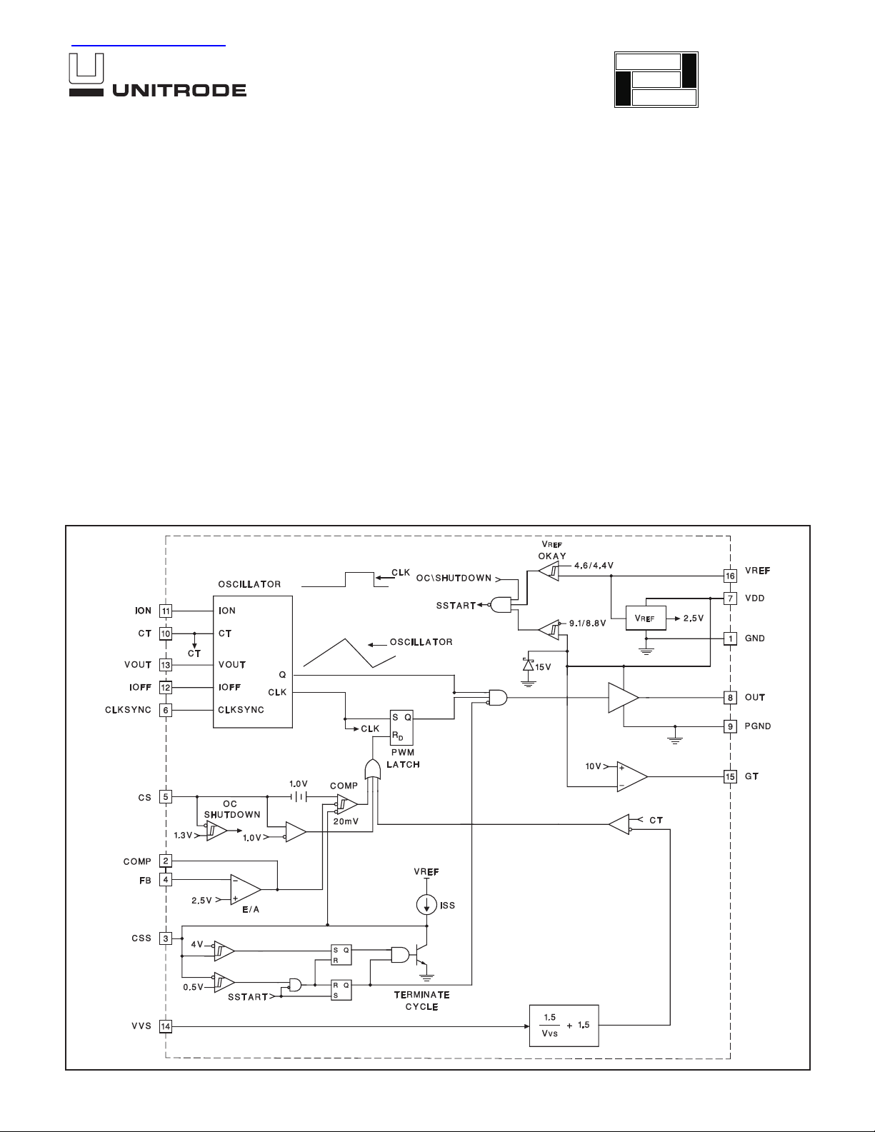
BLOCK DIAGRAM
SLUS160A - AUGUST 1999
UDG-96026-1
Page 2
ABSOLUTE MAXIMUM RATINGS
Supply Voltage . . . . . . . . . . . . . . . . . . . . . . . . . . . . . . . . . . 15V
Output Sink Current. . . . . . . . . . . . . . . . . . . . . . . . . . . . . . . . 1A
Output Source Current . . . . . . . . . . . . . . . . . . . . . . . . . . . . 0.5A
All Other Pins. . . . . . . . . . . . . . . . . . . . . . . . . . . . . . . . . . . . . 6V
Storage Temperature . . . . . . . . . . . . . . . . . . . –65°C to +150°C
Junction Temperature. . . . . . . . . . . . . . . . . . . –55°C to +150°C
Lead Temperature (Soldering, 10 sec.). . . . . . . . . . . . . +300°C
Currents are positive into, negative out of the specified termi
nal. Consult Packaging Section of Databook for thermal limita
tions and considerations of packages.
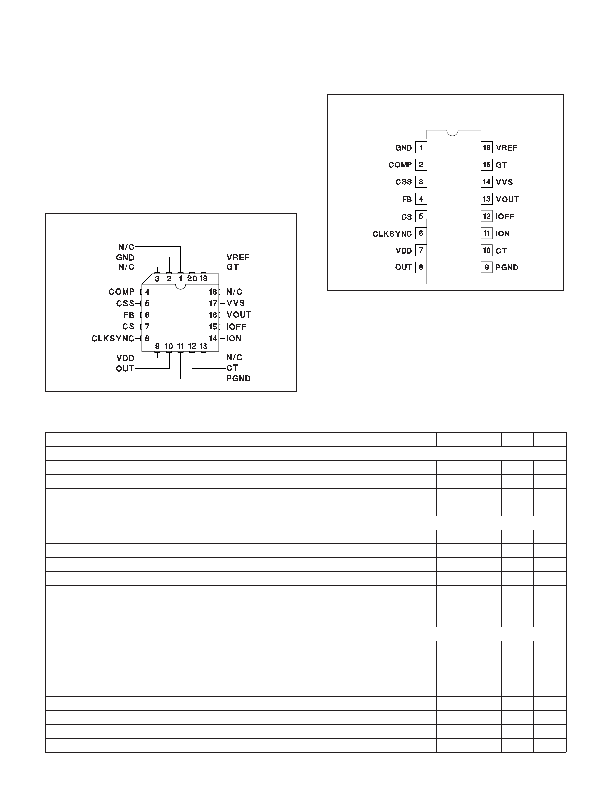
PLCC-20 (Top View)
Q Package
UCC1884
UCC2884
UCC3884
CONNECTION DIAGRAMS
DIL-16, SOIC-16 (Top View)
J, N or D Packages
-
-
ELECTRICAL CHARACTERISTICS: Unless otherwise specified, these specifications apply for TA = –55°C to 125°C for the
UCC1884, –40°C to 85°C for the UCC2884, and 0°C to 70°C for the UCC3884, CT = 220pF, RON= 53k, R
VREF, VVS = 0V, CSS = 2.5nF, VDD = 11V, Output no load, TA=TJ.
PARAMETER TEST CONDITIONS MIN TYP MAX UNITS
5V Reference Section
VREF I
= 0mA 4.86 5 5.14 V
REF
Line Regulation VDD = 10V to 12V 1 10 mV
Load Regulation 0 < I
< 5mA 1 20 mV
REF
Short Circuit I VREF = 0V 15 45 mA
Oscillator Section
Accuracy V
OUT=VREF
360 400 440 kHz
Foldback Frequency VOUT = 0.75V 200 230 260 kHz
CLKSYNC Output High 4.8 5 5.2 V
CLKSYNC Output Low 0.0 0.4 V
CLKSYNC Sink Current CLKSYNC = 1V 1.2 2.2 mA
CLKSYNC Source Current CLKSYNC = 3V –0.2 –0.1 mA
CLKSYNC Input Threshold CLKSYNC from 5V to 0V (Edge Detect) 2.5 3.0 3.5 V
Error Amplifier Section
I
B
Total Bias Current; Regulating Level –1 1 µA
FB Voltage FB = COMP 2.43 2.5 2.57 V
VO 50 90 dB
A
GBW F = 100kHz (Note 1) 2.5 5 MHz
Output Source Current FB = 2.3V, COMP = 2.5V –0.6 –1.2 mA
Output Sink Current FB = 2.7V, V
V
OL
V
OH
IO= 100µA 0.3 0.9 V
IO= –100µA 2.7 3.1 3.5 V
= 1V 0.250 1.5 mA
COMP
= 38k, VOUT =
OFF
2
Page 3
UCC1884
UCC2884
UCC3884
ELECTRICAL CHARACTERISTICS: Unless otherwise specified, these specifications apply for TA = –55°C to 125°C for the
UCC1884, –40°C to 85°C for the UCC2884, and 0°C to 70°C for the UCC3884, CT = 220pF, RON= 53k, R
VREF, VVS = 0V, CSS = 2.5nF, VDD = 11V, Output no load, TA=TJ.
PARAMETER TEST CONDITIONS MIN TYP MAX UNITS
PWM Section
Minimum Duty Cycle FB = 3V, CS = 0V 0 %
Maximum Duty Cycle FB = 0V, CS = 0V 75 78 81 %
Current Sense Section
Input Bias Current (CS) 3.0 µA
CS Shutdown Threshold 1.235 1.3 1.365 V
CS Shutdown Hysteresis 20 mV
CS Over Current Threshold 0.95 1 1.05 V
Current/Fault Section
Soft Start Charge Current –10 –20 –30 µA
Soft Start Discharge Current 10 20 30 µA
V
OL
Soft Start Complete Threshold 3.6 4 4.4 V
Soft Start Restart Threshold 0.4 0.5 0.6 V
Volt Second Clamp
Duty Cycle VVS = 1.4V, T
VVS = 3.6V, T
VVS = 3.6V, T
VVS = 3.6V, T
I
B
VVS = 3.7V –1 +1 µA
= 0°C to 70°C 53.8 56.8 59.8 %
A
= –55°C to 125°C 19.8 22 26.0 %
A
= –40°C to 85°C 20.9 22 25.0 %
A
= 0°C to 70°C 21 22 23 %
A
Output Stage
Output Low Saturation I
Output High Saturation I
UVLO Output Low Saturation I
= 100mA 0.5 0.9 V
OUT
= –50mA 0.5 0.9 V
OUT
= –200mA (Note 1) 1.9 V
I
OUT
= 20mA, VDD = 0V 0.7 1.2 V
OUT
Rise Time CL = 1nF 50 70 ns
Fall Time CL = 1nF 30 50 ns
Undervoltage Lockout
Turn-On Threshold Voltage 8.4 8.9 9.4 V
Hysteresis 200 600 1000 mV
Startup Regulator
Regulated VDD Voltage 9.5 10 10.5 V
VDD Override Threshold 10.7 V
Overall
Range 14.5 V
V
DD
(run) f = 400kHz 2 5 10 mA
I
DD
I
Startup Current VDD = 5.4V 100 250 µA
DD
VDD Clamp IDD = 10mA 12 13.5 15 V
= 38k, VOUT =
OFF
050mV
Note 1: Guaranteed by design. Not 100% tested in production.
3
Page 4

PIN DESCRIPTIONS
CLKSYNC: An edge triggered active low TTL signal to
this pin synchronizes the oscillator to an external clock.
When VOUT decreases below 3.0V, the frequency
foldback circuit is activated and the controller becomes
unsynchronized. When VOUT exceeds 3.0V, the
controller resynchronizes to the external clock.
COMP: The output of the voltage error amplifier used for
compensation. The output is clamped to 3.0V minimum.
CS: Current sense input. This pin accepts a voltage
proportional to converter inductor current. The voltage at
CS is compared to the output of the compensated error
amplifier to control the on-time of the switch. Voltage
mode control can be realized by driving this pin with a
fixed sawtooth ramp. Voltage feedforward is achieved by
making the peak of this ramp proportional to the input
voltage.
CSS: A capacitor, C
time for the power up sequence. This function is also
used when an overcurrent fault occurs. As CSS is
charged, the PWM comparator uses the lowest of either
the voltage at CSS or the error amplifier output voltage to
determine the duty cycle. The duty cycle, therefore,
slowly increases during the soft start cycle. The faults
that cause CSS to discharge and shutdown the controller
are the logical OR of VREF below 4.4V or VDD below
8.8V. If a fault is still present when CSS is discharged
below 0.5V, the supply remains off until the fault is
cleared. The soft start time is determined by:
T=3.5•
SS
where ISS is 20µA. A current limit terminates the present
cycle. It does not generate a soft start cycle.
CT: A capacitor, CT to ground, is charged and
discharged creating the oscillator waveform. This
waveform varies between 1.5V and 3.5V. The operating
frequency is determined by:
f=
R
C•
T
The ratio of the time duration of the positive sloped
portion of the CT voltage waveform to the period gives
the maximum duty cycle.
FB: The inverting input of the voltage amplifier used to
sense the output voltage. The non-inverting input of the
error amplifier is internally connected to 2.5V.
SS, to ground programs the soft start
C
SS
I
SS
4.4
R
3.5
ON OFF
+
1.5
UCC1884
UCC2884
UCC3884
GND: The ground pin internally used for all the amplifiers
and as the return for all resistor and capacitor
connections to the UCC3884.
GT: Used to drive an external depletion-mode MOSFET
for the housekeeping power supply. The MOSFET is
turned off when the bootstrap winding voltage exceeds
10V. There is 300mV of hysteresis around the 10V
turn-off voltage to prevent oscillation. See Typical
Application.
IOFF: A resistor, R
discharge current of the timing capacitor C
variable discharge current which determines the negative
slope of the oscillator voltage waveform at CT. The
discharge time is dependent on the voltage at the VOUT
pin. The discharge current is given by I
VOUT/R
OFF. The VOUT pin is internally clamped to 3.5V
maximum.
ION: A resistor, RON, to ground programs the charge
current of the timing capacitor, C
positive slope of the oscillator waveform. The charge
time is constant and corresponds to the maximum output
on-time at OUT. The charge current equation is I
1.5V/R
ON. When required the linear positive slope of the
CT voltage could be buffered and used to provide slope
compensation into the CS pin.
OUT: The output of the controller. The peak source
current is 0.5A and the peak sink current is 1.0A. The
faults listed under the CSS description turn off this
output.
PGND: The power ground pin is used as the return for
the output transistor drive stage.
VDD: The input voltage of the chip. A low ESR and ESL
ceramic capacitor from this pin to GND should be used
to bypass internal switching transients.
VOUT: This pin accomplishes frequency foldback by
controlling the discharge current for the oscillator C
capacitor. A dc voltage proportional to the output voltage
is connected to this pin. To startup with zero output
voltage the user should tie a resistor between VREF and
VOUT. The value depends on the lowest desired
operating frequency. When VOUT decreases below 3.5V
the frequency decreases by reducing the discharge
current I
OFF. When VOUT increases, the frequency
increases by increasing the discharge current. The
maximum operating frequency occurs when VOUT =
3.5V. The C
T charge time is constant to guarantee a
maximum output duty cycle. This pin must be above
3.0V to allow synchronization to occur.
OFF, to ground, programs the
T. This is a
OFF =
T, which generates the
ON =
T
4
Page 5

PIN DESCRIPTIONS (cont.)
VREF: This pin is the output of the 5V regulated
reference. Bypass this pin with a low ESR and ESL
ceramic capacitor (e.g., 0.47µF).
VVS: Provides a programmable duty cycle clamp which
is dependent upon the input voltage. A resistor divider
network reduces the input voltage supplied to VVS. The
APPLICATION INFORMATION
Theory of Operation
The UCC3884 current mode PWM controller contains a
programmable oscillator which includes the ability to
synchronize multiple PWMs. The positive and negative
sloped portions of the oscillator waveform (measured at
CT), have time intervals that are set by external resistors
at ION and IOFF. The operating frequency is inversely
proportional to the timing capacitor. The negative sloped
portion of the oscillator waveform is extended in time as
the measured output voltage decreases providing
protection during output faults. The power supply output
voltage and the voltage from VREF are fed back to
VOUT. When the output voltage decreases, the voltage
at VOUT also decreases. As VOUT decreases below
3.5V, the operating frequency decreases. This reduction
in frequency allows the duty cycle to decrease below
what the CS to OUT delay would otherwise permit. This
is referred to as frequency foldback. An output short
circuit or overload causes the converter to enter the
frequency foldback mode. Synchronization to other
controllers can only occur during normal operation, that
is, when VOUT is greater than 3.0V.
GT is provided to turn off an external depletion-mode
MOSFET after startup when the bootstrap winding
exceeds 10V. This depletion-mode MOSFET is used in
the housekeeping section of the converter to simplify
startup biasing circuitry. The amplifier that drives this
MOSFET has 300mV of hysteresis to avoid oscillation
during power up.
An accurate programmable volt-second technique
clamps the duty cycle. The duty cycle limit is inversely
proportional to input voltage and a resistor divider
network is used to program the proportionality constant.
At a given input voltage and constant load, under closed
loop control, the operating duty cycle is a fixed value.
The volt-second clamp duty cycle may then be set
somewhat higher than this operating duty cycle. For
other input voltages, the volt-second clamp will still
exceed the steady state operating duty cycle. This allows
normal closed loop operation of the converter. It is during
UCC1884
UCC2884
UCC3884
IC determines the reciprocal of the voltage at VVS and
scales the result. The voltage is then compared to the
oscillator waveform to clamp the duty cycle. The purpose
of this clamp is to reduce the likelihood of saturating the
isolation transformer during unusual line or load condi
tions.
a load transient (a fault such as a momentary short
circuit) as the error amplifier increases the duty cycle,
that when the volt-second clamp accurately limits the
maximum volt-seconds. This ensures that the
transformer does not saturate during a fault which can
fail the power supply. After the fault is removed the
converter resumes closed loop control.
CSS is provided which allows the UCC3884 to be
disabled with an external transistor. The increasing pulse
width at OUT during soft start should be programmed to
be less than the pulse width of the duty cycle limit that
the frequency foldback circuitry creates. The frequency
foldback circuit will be in effect during soft start since the
output voltage fed back to VOUT is less than 3.5V.
Designing the circuit in this fashion allows a proper
startup sequence.
The current sense feedback pin has an overcurrent
protection feature which forces a soft start cycle only if
the IC is not currently in a soft start cycle. A 1V bias at
the PWM comparator’s non-inverting input and a reset
dominant PWM latch permit zero duty cycle operation.
The error amplifier has a wide gain-bandwidth product
and its non-inverting input is internally set to 2.5VDC.
Oscillator
The oscillator has charge and discharge currents pro
grammed with resistors to ground from ION and IOFF re
spectively, as seen on the Oscillator Block Diagram (Fig.
1). This generates a linear sawtooth waveform on CT.
Frequency foldback is accomplished by the level shifted
output voltage controlling the VOUT voltage which de
creases the discharge current and the frequency.
Synchronization is accomplished by coupling the fastest
oscillator CLKSYNC signal as shown on the Oscillator
Synchronization Diagram (Fig. 2). The fastest (master)
CLKSYNC pin will couple a negative pulse into the
slower (slave) CLKSYNC pins forcing the slaves’ CT pins
to quickly discharge as shown on the Oscillator Wave
form diagram (Fig. 3).
-
-
-
-
-
5
Page 6

APPLICATION INFORMATION (cont.)
1.5V
ION
11
UCC1884
UCC2884
UCC3884
V
REF
CLK
10CT
IOFF
13
12
3.5V
14
SYNCEN
3V
VOUT
Figure 1. UCC3884 oscillator.
3.5V
V
REF
8.8X
1.5V
SQ
QR
6 CLKSYNC
3.0V
SYNCEN
UDG-99088
Figure 2. Oscillator synchonization connection
diagram.
UDG-96027
UDG-96028-1
Figure 3. Oscillator waveforms.
6
Page 7

APPLICATION INFORMATION (cont.)
The following explains two synchronization techniques:
1. If the user does not care which unit is the master,
then the oscillator frequencies are designed as accu
rate as necessary and one unit will become the mas
ter and synchronize the remaining units. The user
will never know exactly which unit will be themaster
upon power up.
2. If the user does care which unit is the master, a unit
should be identified as the master, and the frequency
UCC1884
UCC2884
UCC3884
and maximum duty cycle clamp should be pro
grammed accordingly. The ROFF resistor which pro
-
-
grams the slave units oscillator discharge ramp
should be between 50% and 100% of the ROFF re
sistor which programs the master. This guarantees
that if a slave unit tries to synchronize the master,
the master frequency will still be faster than the slave
frequency and the master will synchronize all the re
maining units.
-
-
-
-
Figure 4. Typical application.
UNITRODE CORPORATION
7 CONTINENTAL BLVD. • MERRIMACK, NH 03054
TEL. (603) 424-2410 FAX (603) 424-3460
UDG-96032-1
7
Page 8

IMPORTANT NOTICE
T exas Instruments and its subsidiaries (TI) reserve the right to make changes to their products or to discontinue
any product or service without notice, and advise customers to obtain the latest version of relevant information
to verify, before placing orders, that information being relied on is current and complete. All products are sold
subject to the terms and conditions of sale supplied at the time of order acknowledgement, including those
pertaining to warranty, patent infringement, and limitation of liability.
TI warrants performance of its semiconductor products to the specifications applicable at the time of sale in
accordance with TI’s standard warranty. Testing and other quality control techniques are utilized to the extent
TI deems necessary to support this warranty . Specific testing of all parameters of each device is not necessarily
performed, except those mandated by government requirements.
CERTAIN APPLICATIONS USING SEMICONDUCTOR PRODUCTS MAY INVOLVE POTENTIAL RISKS OF
DEATH, PERSONAL INJURY, OR SEVERE PROPERTY OR ENVIRONMENTAL DAMAGE (“CRITICAL
APPLICATIONS”). TI SEMICONDUCTOR PRODUCTS ARE NOT DESIGNED, AUTHORIZED, OR
WARRANTED TO BE SUITABLE FOR USE IN LIFE-SUPPORT DEVICES OR SYSTEMS OR OTHER
CRITICAL APPLICA TIONS. INCLUSION OF TI PRODUCTS IN SUCH APPLICATIONS IS UNDERST OOD TO
BE FULLY AT THE CUSTOMER’S RISK.
In order to minimize risks associated with the customer’s applications, adequate design and operating
safeguards must be provided by the customer to minimize inherent or procedural hazards.
TI assumes no liability for applications assistance or customer product design. TI does not warrant or represent
that any license, either express or implied, is granted under any patent right, copyright, mask work right, or other
intellectual property right of TI covering or relating to any combination, machine, or process in which such
semiconductor products or services might be or are used. TI’s publication of information regarding any third
party’s products or services does not constitute TI’s approval, warranty or endorsement thereof.
Copyright 1999, Texas Instruments Incorporated
 Loading...