

Page 1
查询UCC1858供应商
High Efficiency, High Power Factor Preregulator
UCC1858
UCC2858
UCC3858
PRELIMINARY
FEATURES
• Programmable PWM Frequency
Foldback for Higher Efficiency at Light
Loads
• Leading Edge PWM for Reduced
Output Capacitor Ripple Current
• Controls Boost PWM to Near Unity
Power Factor
• World Wide Operation without
Switches
• Accurate Power Limiting
• Synchronizable Oscillator
• 100µA Startup Supply Current
• Low Power BCDMOS
• 12V to 18V Operation
DESCRIPTION
The UCC3858 provides all of the control functions necessary for active
power factor corrected preregulators which require high efficiency at low
power operation. The controller achieves near unity power factor by
shaping the AC input line current waveform to correspond to the AC input
line voltage using average current mode control.
The operation of the UCC3858 closely resembles that of previously designed Unitrode PFC parts with additional features to allow higher efficiency boost converter operation at light loads. This is accomplished by
linearly scaling back the PWM frequency when the output of the voltage
error amplifier drops below a predetermined user programmable level indicating a light load condition. The frequency is scaled back by reducing
the charging current for the CT ramp (in proportion to the output power),
and increasing the dead time. There is also an instantaneous reset input
to pull the IC out of foldback mode quickly when the load comes back up.
The PWM technique used in the UCC3858 is leading edge modulation.
When combined with the more conventional trailing edge modulation on
the downstream converter, this scheme offers the benefit of reduced ripple current on the bulk storage capacitor. The oscillator is designed for
easy synchronization to the downstream converter. A simple synchronization scheme can be implemented by connecting the PWM output of
the downstream converter to the SYNC pin.
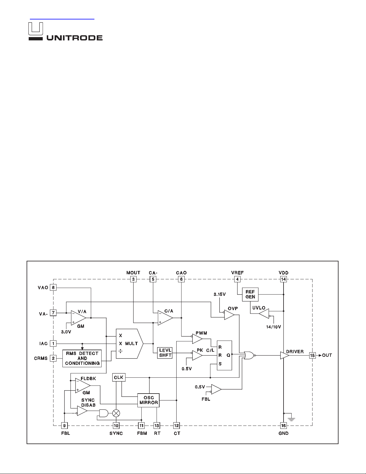
BLOCK DIAGRAM
(continued)
03/99
UDG-96191-1
Page 2
ABSOLUTE MAXIMUM RATINGS
Supply Voltage VDD. . . . . . . . . . . . . . . . . . . . . . . . . . . . . . 18V
Gate Drive Current
Continuous . . . . . . . . . . . . . . . . . . . . . . . . . . . . . . . . . . 0.2A
Pulsed . . . . . . . . . . . . . . . . . . . . . . . . . . . . . . . . . . . . 500mA
Input Current IAC . . . . . . . . . . . . . . . . . . . . . . . . . . . . . . 200mA
Power Dissipation. . . . . . . . . . . . . . . . . . . . . . . . . . . . . . . . . 1W
Storage Temperature . . . . . . . . . . . . . . . . . . . −65°C to +150°C
Junction Temperature. . . . . . . . . . . . . . . . . . . −55°C to +150°C
Lead Temperature (Soldering, 10 Sec.). . . . . . . . . . . . . +300°C
Analog Inputs
Maximum Forced Voltage . . . . . . . . . . . . . . . . –0.3V to 11V
Unless otherwise indicated, voltages are reference to ground and currents are positive into, negative out of the specified terminal. Pulsed is
defined as a less than 10% duty cycle with a maximum duration of
500ns. Consult Packaging Section of Databook for thermal limitations
and considerations of packages.
DESCRIPTION (cont.)
Controller improvements include an onboard peak detector for the input line RMS voltage, an integrated
overcurrent shutdown, overvoltage shutdown and significantly lower quiescent operating current. The peak detector eliminates an external 2-pole low pass filter for
RMS detection. This simplifies the converter design as
well as providing an approximate 6X improvement in input line transient response. The current signal is extracted from the current error amplifier input to provide a
cycle-by-cycle peak current limit. Low startup and operating currents which are achieved through the use of
UCC1858
UCC2858
UCC3858
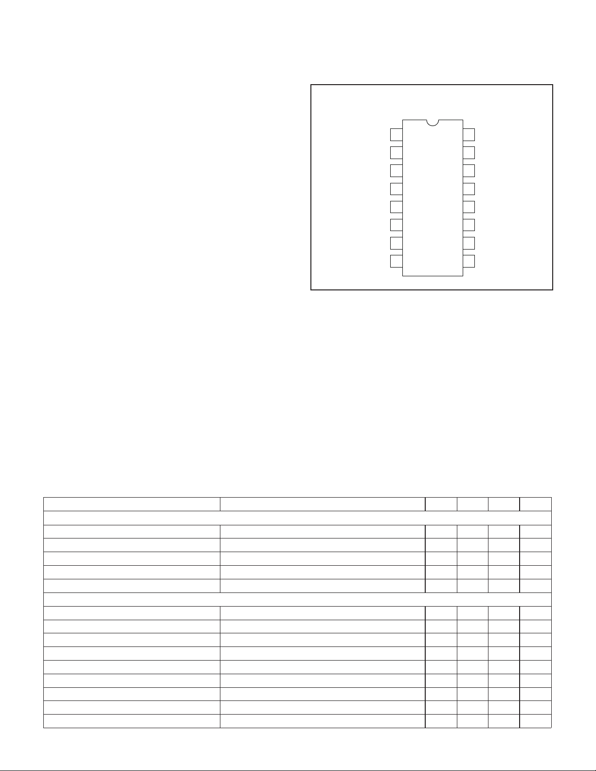
CONNECTION DIAGRAM
DIP-16, SOIC-16 (TOP VIEW)
J, N,DW Packages
IAC
1
VREF
CA–
CAO
VA–
VAO
2
3
4
5
6
7
8
CRMS
MOUT
Unitrode’s BCDMOS process simplify the bootstrap
supply design as well as minimize losses in the control
circuit. A transconductance voltage error amplifier allows
output voltage sensing for internal overvoltage protection.
Additional features include: undervoltage lockout for reliable off-line startup, a precision 7.5V reference, and a
precision RMS detection and signal conditioning circuit.
Chip shutdown can be attained by bringing the FBL pin
below 0.5V.
16
GND
15
OUT
14
VDD
13
RT
12
CT
11
FBM
10
SYNC
9
FBL
ELECTRICAL CHARACTERISTICS:
UCC3858, –40°C to +85°C for the UCC2858, and –55°C to +150°C for the UCC1858, V
96k, I
= 100µA, TA= TJ.
IAC
Unless otherwise stated, these specifications apply for TA= 0°C to 70°C for the
= 12V, RT= 24k, CT= 330pF, R
VDD
PARAMETER TEST CONDITIONS MIN TYP MAX UNITS
Overall
Supply Current, Off V
CAO
, V
= 0V, VDD= UVLO – 0.3V 100 250 µA
VAO
Supply Current, On FBL = 0V 2 3.5 5 mA
VDD Turn-On Threshold 12 13.5 15.5 V
VDD Turn-Off Threshold 10 V
UVLO Hysteresis 3.2 3.5 3.8 V
Voltage Amplifier
Input Voltage T
= 25°C 2.95 3 3.05 V
A
Over Voltage Protection Volts Above VA– Input Voltage 0.12 0.14 0.16 V
VA– Bias Current –0.5 –1 µA
Open Loop Gain V
= 2V to 5V 45 50 dB
OUT
VAO High Load = –25µA 5.7 6 6.3 V
VAO Low Load = 25µA 0.3 0.5 V
Output Source Current V
Output Sink Current V
Transconductance I
– = 2.8V –50 µA
VA
– = 3.2V 50 µA
VA
= ± 50µA 400 600 1000 µS
OUT
2
FBM
=
Page 3
UCC1858
UCC2858
UCC3858
ELECTRICAL CHARACTERISTICS:
UCC3858, –40°C to +85°C for the UCC2858, and –55°C to +150°C for the UCC1858, V
96k, I
= 100µA, TA= TJ.
IAC
Unless otherwise stated, these specifications apply for TA= 0°C to 70°C for the
= 12V, RT= 24k, CT= 330pF, R
VDD
PARAMETER TEST CONDITIONS MIN TYP MAX UNITS
Current Amplifier
Input Offset Voltage V
Input Bias Current V
Input Offset Current V
Open Loop Gain V
CMRR V
CAO High V
CAO Low V
= 0V, V
CM
= 0V, V
CM
= 0V, V
CM
= 0V, V
CM
= 0V to 1.5V, V
CM
= 0V, V
–
CA
= 1V, V
–
CA
= 3V –3 0 3 mV
CAO
= 3V –6.5 –5 µA
CAO
= 3V –0.5 0.0 0.5 µA
CAO
= 2V to 5V 80 90 dB
CAO
= 3V 65 80 dB
CAO
= 1V, IL= –50µA 6.5 7 7.5 V
MOUT
= 0V, IL= 1mA 0.2 0.3 V
MOUT
Maximum Output Source Current –130 –150 µA
Voltage Reference
Output Voltage I
= 0mA, TA= 25°C 7.313 7.5 7.688 V
REF
Over Temperature, UCC3858 7.294 7.5 7.707 V
Over Temperature, UCC2858, UCC1858 7.239 7.5 7.762 V
Load Regulation I
Line Regulation V
Short Circuit Current V
= 0mA to 2mA 3 5 mV
REF
= 12V to 16V 30 mV
DD
= 0V 35 50 mA
REF
Oscillator
Initial Accuracy TA= 25°C 90 100 110 kHz
Voltage Stability V
= 12V to 16V 1 %
DD
Total Variation Line, Temperature 80 120 kHz
Ramp Amplitude (p-p) Oscillator Free Running, VAO = 5.5V 3.3 3.5 3.7 V
Ramp Peak Voltage Oscillator Free Running, VAO = 5.5V 4.4 4.6 4.8 V
Peak Current Limit
PKLMT Threshold Voltage (V
CA
–)–V
MOUT
350 450 550 mV
PKLMT Hysteresis 100 200 mV
PKLMT Propagation Delay 1 µs
Multiplier Section
High Line, Low Power I
High Line, High Power I
Low Line, Low Power I
Low Line, High Power I
IAC Limited I
Gain Constant I
Zero Current I
Power Limit (V
• IMO)I
CRMS
= 100µA, V
AC
= 100µA, V
AC
= 20µA, V
AC
= 20µA, V
AC
= 20µA, V
AC
= 100µA, V
AC
= 20µA, V
AC
=100µA, V
I
AC
= 20µA, V
AC
CRMS
CRMS
CRMS
CRMS
CRMS
CRMS
CRMS
CRMS
CRMS
= 3.5V, VA
= 3.5V, VA
= 0.75V, VA
= 0.75V, VA
= 0.4V, VA
= 3.5V, VA
= 0.75V, VA
= 3.5V, VA
= 0.75V, VA
= 1.25V 1 µA
OUT
= 5.5V 15 µA
OUT
= 1.25V 4 µA
OUT
= 5.5V 64 µA
OUT
= 5.5V 64 µA
OUT
= 5.5V 2.5 1/V
OUT
= 5.5V (Note 1) 0 µA
OUT
= 5.5V (Note 1) 0 µA
OUT
= 5.5V 45 µW
OUT
PWM Frequency Foldback
FBL Input Current –500 –100 nA
FBL Output Disable 0.5 V
Foldback Minimum Frequency R
= 100k 25 30 kHz
FBM
FBM Foldback Override 1.5 1.75 V
FBM
=
3
Page 4
UCC1858
UCC2858
UCC3858
ELECTRICAL CHARACTERISTICS: Unless otherwise stated, these specifications apply for T
UCC3858, –40°C to +85°C for the UCC2858, and –55°C to +150°C for the UCC1858, V
96k, I
Gate Driver
Note1: M
= 100µA, TA= TJ.
IAC
PARAMETER TEST CONDITIONS MIN TYP MAX UNITS
Pull Up Resistance I
Pull Down Resistance I
Output Rise Time C
Output Fall Time C
current with contributions form CA+ and peak limit level shift subtracted out.
OUT
= 100mA 7 Ω
OUT
= –100mA 3.5 Ω
OUT
= 1nF, RS= 10Ω 25 ns
LOAD
= 1nF, RS= 10Ω 20 ns
LOAD
= 12V, RT= 24k, CT= 330pF, R
VDD
PIN DESCRIPTIONS
CA–: (Current Amplifier Inverting Input) This input and
the non-inverting input MOUT remain functional down to
GND.
CAO: (Current Amplifier Ouput) Output of a wide bandwidth amplifier that senses line current and commands
the pulse width modulator (PWM) to force the correct current. This output can swing close to GND, allowing the
PWM to force zero duty cycle when necessary.
CRMS: (RMS Measurement Capacitor) A capacitor connected between CRMS and GND enables averaging of
the AC line voltage over a half cycle. IAC current is internally mirrored to provide charging current for CRMS.
CT: (Oscillator Timing Capacitor) A capacitor from CT to
GND will set the free-running PWM oscillator frequency
according to:
0814.
f
=
RC
•
TT
FBL: (Frequency Foldback Level Select) Selects the level
of the voltage error amplifier output at which frequency
foldback begins. A chip shutdown can be attained by
bringing the foldback level pin to below 0.5V.
FBM: (Minimum Frequency Reference) A resistor between this pin and VREF is used to set the minimum frequency during foldback mode. Once the value of R
C
are determined, use
T
R
FBM
to find the value of R
foldback frequency to f
0857.
=
Cf
•
TMIN
R
−
T
which will set the minimum
FBM
This pin also incorporates a
MIN.
T
and
foldback override which enables the part to return quickly
to normal operating mode when the load comes back up.
To override foldback mode, force this pin below 1.5V with
an open collector.
GND: (Ground) All voltages measured with respect to
ground. VDD and VREF should be bypassed directly to
GND with a 0.1µF or larger ceramic capacitor. The timing
capacitor discharge current also returns to this pin, so
the lead from CT to GND should be as short and direct
as possible.
IAC:(Input AC Current) This input to the analog multiplier
is a current. The multiplier is tailored for very low distortion from this current input (I
some bypassing to GND for noise filtering (<470pF).
MOUT: (Multiplier Output) The output of the analog multiplier and the non-inverting input of the current amplifier
are connected together at MOUT. As the multiplier output
is a current, this is a high impedance input so the amplifier can be configured as a differential amplifier to reject
ground noise. The voltage at this pin is also used to implement peak current limiting.
OUT: (Gate Drive Output) The output of the PWM is a totem pole MOSFET gate driver. A series gate resistor of
at least 5Ω is recommended to prevent interaction between the gate impedance and the output driver that
might cause the gate drive to overshoot excessively.
RT: (Oscillator Timing Resistor) A resistor from RT to
GND is used to program oscillator discharge current.
SYNC: (Oscillator Synchronization Input) Allows the PFC
to be synchronized to a trailing edge modulator in the
DC-DC stage. A synchronization pulse can be generated
from the positive output edge of the downstream regulator and applied to this pin. The internal clock is reset
(charged up) on the rising edge of the SYNC input.
VA–: (Voltage Amplifier Inverting Input) This pin is normally connected to the boost converter output through a
divider network. It also is an input to the overvoltage
comparator where by the output is terminated if this pin’s
voltage exceeds 3.15V.
VAO: (Voltage Amplifier Output) Output of the
transconductance amplifier that regulates output voltage.
The voltage amplifier output is internally limited to approximately 6V for power limiting. It is also used to determine the frequency foldback mode. Compensation
network is connected from this pin to GND.
= 0°C to 70°C for the
A
) to MOUT. Requires
IAC
FBM
=
4
Page 5

PIN DESCRIPTIONS (cont.)
VDD: (Positive Supply Voltage) Connect to a stable
source of at least 20mA between 13V and 17V for normal
operation. Bypass VDD directly to GND to absorb supply
current spikes required to charge external MOSFET gate
capacitance. To prevent inadequate gate drive signals,
the output devices will be inhibited unless V
VDD
exceeds
the upper undervoltage lockout voltage threshold and remains above the lower threshold.
APPLICATION INFORMATION
The UCC3858 is designed to optimize the implementation of power factor corrected boost converters in low to
medium power applications where light load efficiency is
critical. While basic configuration of the UCC3858 is similar to the industry standard UC3854 series controllers,
several distinguishing features have been added. A typical application circuit is shown along with a diagram
showing how the UCC3858 can be used with the downstream converter to achieve optimum performance.
Chip Bias Supply and Startup
The UCC3858 is implemented using Unitrode’s
BCDMOS process allowing minimal startup (60µA typical) and operating (3.5mA typical) supply currents. This
results in significantly lower power consumption in the
trickle charge resistor used to startup the IC, increasing
the system efficiency at light loads. Lower supply currents, coupled with the wide undervoltage lockout hysteresis (13.75V on, 10V off) provide the opportunity to
operate both stages from the same startup and bootstrap
supply as shown in the typical application drawing.
Oscillator and Frequency Foldback at Light Loads
The oscillator of the UCC3858 is set up to operate either
synchronously with the downstream converter or as a
stand alone oscillator. A simplified block diagram of the
oscillator and associated circuitry is shown in Fig. 2 and
the related waveforms are shown in Fig. 3a - 3c. A rising
edge at the SYNC pin initiates the clock cycle by charging up the CT pin with a nominal internal current of
I
CHnom (=19 •IDIS). Once the high threshold of the ramp
(4.5V) is crossed, the internal latch is set and the CT pin
starts discharging at a rate (I
on the RT pin. In the absence of a SYNC pulse, C
charges all the way to the ramp low threshold (1V) and
that sets the free running frequency of the oscillator as
given by equation 1. In applications where synchronization is used, the R
values should be chosen so that
T,CT
the free running frequency is always lower than the synchronization frequency.
19203
f
=• •
351.
RC
•
TT
=3/RT) set by the resistor
DIS
dis-
T
(1)
UCC1858
UCC2858
UCC3858
VREF: (Reference Voltage) VREF is the output of an ac-
curate 7.5V voltage reference. This output is capable of
delivering 10mA to peripheral circuitry and is internally
short circuit current limited. VREF is disabled and will remain at 0V when V
a 0.1µF or larger ceramic capacitor for best stability.
When VAO falls below the threshold level set by FBL, the
oscillator goes into frequency foldback mode and disables synchronization. The frequency foldback is
achieved by reducing the oscillator charging current as
the power level (and VAO voltage) falls. As shown in Fig.
2, the difference between VAO and FBL regulates current I
Csub which subtracts the current available for charg-
ing C
. The effective charge current into the capacitor is
T
given by (I
CHnom-ICsub
the low frequency range (e.g. audio), the charge current
should not be allowed to go very low.Minimum frequency
of the controller is programmed by the current I
ing into pin FBM which sets the minimum charging current. The value of R
frequency is given by:
R
FBM
3351
=•
.
Fig. 4 shows the characteristic curves for the frequency
foldback. When the converter comes out of the low
power mode, the time taken to restore normal mode operation (return to nominal or synchronized frequency operation) must be minimized. Given that the voltage error
amplifier response is very slow in PFC circuits, the VAO
pin change is not the best indicator of change in load
conditions. UCC3858 provides a solution where the normal mode can be restored instantaneously when FBM is
pulled below 1.5V. A typical interface would involve the
output of the error amplifier of the downstream converter
(with proper buffering and filtering) driving an npn switch
that pulls FBM down to GND. The buffer and filter should
ensure that the switch is turned on only when the error
amplifier of downstream converter is saturated high for a
preset duration indicating a droop in output voltage from
increased load. The FBM input can also be permanently
pulled low to disable the frequency foldback mode completely, while still using the other features of UCC3858.
FBL pin also acts as a chip disable input when it is
brought below 0.5V.
is low.Bypass VREF to GND with
VDD
). To avoid converter operation in
to set the desired minimum
FBM
R
–
fC
•
MIN T
T
MIN flow-
(2)
5
Page 6

APPLICATION INFORMATION (cont.)
UCC1858
UCC2858
UCC3858
UDG-97120-1
* Pins 4, 9 and 14 need good bypassing to GND for noise immunity. Capacitors C2, C3 and C23 should each consist of a combination of ceramic (0.47
* * L1 can be fabricated with an Allied Signal Amorphous Core MP4510PFC, using a 100 turn (AWG 18) primary and 5 turn secondary.Alternatively, a gapped Ferrite Choke can be used. (Coiltronics CTX-08-13679)
µ
F) and tantalum (4.7µF) capacitors for best results.
Figure 1. UCC3858 Typical application circuit.
6
Page 7

APPLICATION INFORMATION (cont.)
UCC1858
UCC2858
UCC3858
Figure 2. Oscillator block diagram.
SYNC
V
CAO
V
V
OUT
BOOST
DIODE
CURRENT
CT
4.75V
T
S
>1V
V
CAO
V
V
OUT
BOOST
DIODE
CURRENT
CT
UDG-97121-1
4.75V
>1V
T
S
Figure 3a. Oscillator timing waveforms synchronized
to buck (DC/DC) PWM.
Figure 3b. Oscillator timing waveforms stand alone
operation.
7
Page 8

APPLICATION INFORMATION (cont.)
UCC1858
UCC2858
UCC3858
T
4.5V
S
SLOPE=
I
CH
C
V
CAO
V
V
OUT
CLK
BOOST
DIODE
CURRENT
CT
Figure 3c. Frequency foldback mode.
100
% NOMINAL FREQUENCY
80
60
40
20
–1 –2 –30
FBL = VAO(V)
(R
= 24k, CT= 330pF, NOMINALFREQUENCY 100kHz)
T
–4
–5 –6
R
= 10k
FBM
R
= 25k
FBM
R
= 100k
FBM
>1V
T
Figure 4. Frequency foldback characteristics.
Capacitor Ripple Reduction
For a power system where the PFC boost converter is
followed by a DC-DC converter stage, there are benefits
to synchronizing the two converters. In addition to the
usual advantages such as noise reduction and stability,
proper synchronization can significantly reduce the ripple
currents in the boost circuit’s output capacitor. Fig. 5
helps illustrate the impact of proper synchronization by
showing a PFC boost converter together with the simplified input stage of a forward converter. The capacitor current during a single switching cycle depends on the
status of the switches Q1 and Q2 and is shown in Fig. 6.
It can be seen that with a synchronization scheme that
maintains conventional trailing edge modulation on both
converters, the capacitor current ripple is highest. The
greatest ripple current cancellation is attained when the
overlap of Q1 off-time and Q2 on-time is maximized. One
method of achieving this is to synchronize the turn-on of
the boost diode (D1) with the turn-on of Q2. This approach implies that the boost converter’s leading edge is
pulse width modulated while the forward converter is
modulated with traditional trailing edge PWM. The
UCC3858 is designed as a leading edge modulator with
easy synchronization to the downstream converter to facilitate this advantage. Table 1 compares the I
CBrms
for
D1/Q2 synchronization as offered by UCC3858 vs. the
I
CB
for the other extreme of synchronizing the turn-on
rms
of Q1 and Q2 for a 200W power system with a V
BST
of
385V.
UDG-97130-1
Figure 5. Simplified representation of a 2-stage PFC
power supply.
UDG-97131
Switch Sync
Trailing-Edge PWM for
both Boost and Buck
Inverted Switch Sync
Leading-Edge Boost PWM
Trailing-Edge Buck PWM
Figure 6. Timing waveforms for synchronization
scheme.
8
Page 9

APPLICATION INFORMATION (cont.)
Table I. Effects of Sychronization on Boost
Capacitor Current
VIN= 85V VIN= 120V VIN= 240V
D(Q2) Q1/Q2 D1/Q2 Q1/Q2 D1/Q2 Q1/Q2 D1/Q2
0.35 1.491A 0.835A 1.341A 0.663A 1.024A 0.731A
0.45 1.432A 0.93A 1.276A 0.664A 0.897A 0.614A
Table 1 illustrates that the boost capacitor ripple current
can be reduced by about 50% at nominal line and about
30% at high line with the synchronization scheme facilitated by the UCC3858. The output capacitance value can
be significantly reduced if its choice is dictated by ripple
current or the capacitor life can be increased as a result.
In cost sensitive designs where hold-up time is not critical, this is a significant advantage.
An alternative method of synchronization to achieve the
same ripple reduction is possible. In this method, the
turn-on of Q1 is synchronized to the turn-off of Q2. While
this method yields almost identical ripple reduction and
maintains trailing edge modulation on both converters,
the synchronization is much more difficult to achieve and
the circuit can become susceptible to noise as the synchronizing edge itself is being modulated.
Reference Signal (I
Like the UC3854 series, the UCC3858 has an Analog
Computation Unit (ACU) which generates a reference
current signal for the current error amplifier. The inputs to
the ACU are (signals proportional to) instantaneous line
voltage, input voltage RMS information and the voltage
error amplifier output. Unlike prior techniques of RMS
voltage sensing, UCC3858 employs a patent pending
technique to simplify the RMS voltage generation and
eliminate performance degradation caused by the prior
techniques. With the novel technique (shown in Fig. 7),
need for external two pole filter for V
eliminated. Instead, the IAC current is mirrored and used
to charge an external capacitor (C
cle. The voltage on CRMS takes the integrated sinusoidal
shape and is given by equation 3. At the end of the halfcycle, CRMS voltage is held and converted into a 4-bit
digital word for further processing in the ACU. CRMS is
discharged and readied for integration during the next
half cycle. The advantage of this method is that the second harmonic ripple on the V
nated. Such second harmonic ripple is unavoidable with
the limited roll-off of a conventional 2-pole filter and results in a 3rd harmonic distortion in the input current signal. The dynamic response to the input line variations is
also improved as a new V
cycle.
) Generation
MULT
generation is
RMS
) during a half cy-
RMS
signal is virtually elimi-
RMS
signal is generated every
RMS
UCC1858
UCC2858
UCC3858
I
AC
V
Vpk
CRMS
RMS
C
CRMS
CRMS
2
=
()=
••
LINE
V
CRMS
ADC
HOLD
AD
pk
C
RMS
I
AC
pk
C
•ω
RMS
R
AC
IAC
1
4BIT
WORD
•21ωω(–cos )
REGISTER
t
VAO
MULTI
DAC
(X2)
Figure 7. Novel circuit for RMS signal generation.
For proper operation, I
should be selected to be
ACpk
100µA at peak line voltage. For universal input voltage
with peak value of 265 VAC, this means R
= 3.6M. The
AC
noise sensitivity of the IC requires a small bypass capacitor for high frequency noise filtering. The value of this capacitor should be limited to 330pF maximum. The V
value should be approximately 1V at the peak of low line
(80 VAC) to minimize any digitization errors. The peak
value of V
sired C
RMS
at high line then becomes 3.5V. The de-
CRMS
can be calculated from equation 3 to be 90nF
for 50Hz line and 75nF for 60Hz line.
The multiplier output current is given by equation (4) with
K=0.33.
I
MULT
VIK
VAO AC
=
••(–)1
CRMS
2
V
The multiplier peak current is limited to 200µA and the
selected values for IACand V
should ensure that
CRMS
the current is within this range. Another limitation of the
multiplier is that I
current, limiting the minimum voltage on V
can not exceed two times the I
MULT
CRMS
(3a)
(3b)
A
A•B
B
C
C
CRMS
(4)
AC
.
9
Page 10

APPLICATION INFORMATION (cont.)
The discrete nature of the RMS voltage feedforward
means that there are regions of operation where the input voltage changes, but the V
tiplier does not change. The voltage error amplifier
compensates for this by changing its output to maintain
the required multiplier output current. When the output of
the ADC changes, there is a jump in the output of the error amplifier. There is a resultant shift in the foldback frequency if the converter is at light load. However, the
impact of this change is minimal on the overall converter
operation.
Another key consideration with the RMS voltage scheme
is that it relies on the zero-crossing of the I
effective. At very light loads and high line conditions, the
rectified AC does not quite reach zero if a large capacitor
is being used for filtering on the rectified side of the
bridge. In such instances, the feedforward effect does not
take place and the controller functionality is lost. For
UCC3858, the I
current should go below 10µA for the
AC
zero crossing detection to take place. It is recommended
that the capacitor value be kept low enough for the light
load operation or the feedforward be derived directly from
the AC side of the input bridge as shown in the typical
applications circuit.
Gate Drive Considerations
The gate drive circuit in UCC3858 is designed for high
speed power switch drive. It consists of low impedance
pull-up and pull-down DMOS output stages. When operating with high bias voltages, in order to stay within the
SOA of the DMOS output stages, it is recommended that
the gate drive current be limited to 0.5A peak with the
use of external gate resistor. Please see the characteristic curve in Fig. 8 for determining the required external resistance.
40
value fed into the mul-
RMS
signal to be
AC
UCC1858
UCC2858
UCC3858
Current Amplifier Set-up
The multiplier is set-up first by choosing the V
The maximum multiplier output is at low line, full load
conditions. The inductor peak current also occurs at the
same point. The multiplier terminating resistor can be determined using equation 5.
IL R
•
R
MULT
PK SENSE
=
I
MULT
PK
The peak current limiting function provided by the
UCC3858 is integrated into MOUT. The signal on MOUT
is normally maintained at 0V as the (I
MULT•RMULT
cels the voltage drop across the sense resistor with
closed loop operation. During short circuit or transient
startup conditions, the multiplier current can not fully cancel the voltage drop across R
SENSE and the voltage at
MOUT drops below 0V. The internal peak current limit is
activated when MOUT drops below –0.5V. The peak current limit at any operating point is given by:
IR
•+05.
LIM
=
MULT MULT
R
SENSE
I
The current amplifier can be compensated using previously presented techniques, (Application Note U- 134),
summarized here. A simplified high frequency model for
inductor current to duty cycle transfer function is given
by:
∧
idV
()=
LO
=
∧
sL
Gs
id
The gain of the current feedback path at the frequency of
interest (crossover) is given by:
∧
d
R
=••
SENSE
∧
i
L
R
RV
1
Z
ISE
RMS
range.
(5)
) can-
(6)
(7)
(8)
30
)
Ω
20
RS(
10
0
10 12 14 16 18 20
VDD(V)
Figure 8. Reguired series gate resistance as a
function of supply voltage.
Where V
is the ramp amplitude (p-p) which is 3.5V for
SE
UCC3858. Combining equations 7 and 8 yields the loop
gain of the current loop and equating it to 1 at the desired crossover frequency can result in a design value for
R
. The current loop crossover frequency selected using
Z
conventional trade offs. However, it should be ensured
that the current-loop is stable at the minimum switching
frequency under foldback conditions.
10
Page 11

APPLICATION INFORMATION (cont.)
APPLICATION INFORMATION (continued)
UCC1858
UCC2858
UCC3858
Voltage Amplifier Set-up
The voltage amplifier in UCC3858 is a transconductance
type amplifier to allow output voltage monitoring for an
overvoltage condition. The gain of the amplifier, given by
Figure 9. Use of the UCC3858 in a two stage converter to optimize performance.
UNITRODE CORPORATION
7 CONTINENTAL BLVD. • MERRIMACK, NH 03054
TEL. (603) 424-2410 • FAX (603) 424-3460
11
UDG-96192-1
Page 12

IMPORTANT NOTICE
T exas Instruments and its subsidiaries (TI) reserve the right to make changes to their products or to discontinue
any product or service without notice, and advise customers to obtain the latest version of relevant information
to verify, before placing orders, that information being relied on is current and complete. All products are sold
subject to the terms and conditions of sale supplied at the time of order acknowledgement, including those
pertaining to warranty, patent infringement, and limitation of liability.
TI warrants performance of its semiconductor products to the specifications applicable at the time of sale in
accordance with TI’s standard warranty. Testing and other quality control techniques are utilized to the extent
TI deems necessary to support this warranty . Specific testing of all parameters of each device is not necessarily
performed, except those mandated by government requirements.
CERTAIN APPLICA TIONS USING SEMICONDUCTOR PRODUCTS MA Y INVOLVE POTENTIAL RISKS OF
DEATH, PERSONAL INJURY, OR SEVERE PROPERTY OR ENVIRONMENTAL DAMAGE (“CRITICAL
APPLICATIONS”). TI SEMICONDUCTOR PRODUCTS ARE NOT DESIGNED, AUTHORIZED, OR
WARRANTED TO BE SUITABLE FOR USE IN LIFE-SUPPORT DEVICES OR SYSTEMS OR OTHER
CRITICAL APPLICA TIONS. INCLUSION OF TI PRODUCTS IN SUCH APPLICATIONS IS UNDERST OOD TO
BE FULLY AT THE CUSTOMER’S RISK.
In order to minimize risks associated with the customer’s applications, adequate design and operating
safeguards must be provided by the customer to minimize inherent or procedural hazards.
TI assumes no liability for applications assistance or customer product design. TI does not warrant or represent
that any license, either express or implied, is granted under any patent right, copyright, mask work right, or other
intellectual property right of TI covering or relating to any combination, machine, or process in which such
semiconductor products or services might be or are used. TI’s publication of information regarding any third
party’s products or services does not constitute TI’s approval, warranty or endorsement thereof.
Copyright 1999, Texas Instruments Incorporated
 Loading...