

UNITRODE UC1706, UC2706, UC3706 Technical data
查询UC2706供应商
Dual Output Driver
UC1706
UC2706
UC3706
FEATURES
• Dual, 1.5A Totem Pole Outputs
• 40nsec Rise and Fall into 1000pF
• Parallel or Push-Pull Operation
• Single-Ended to Push-Pull Conversion
• High-Speed, Power MOSFET
Compatible
• Low Cross-Conduction Current Spike
• Analog, Latched Shutdown
• Internal Deadband Inhibit Circuit
• Low Quiescent Current
• 5 to 40V Operation
• Thermal Shutdown Protection
• 16-Pin Dual-In-Line Package
• 20-Pin Surface Mount Package
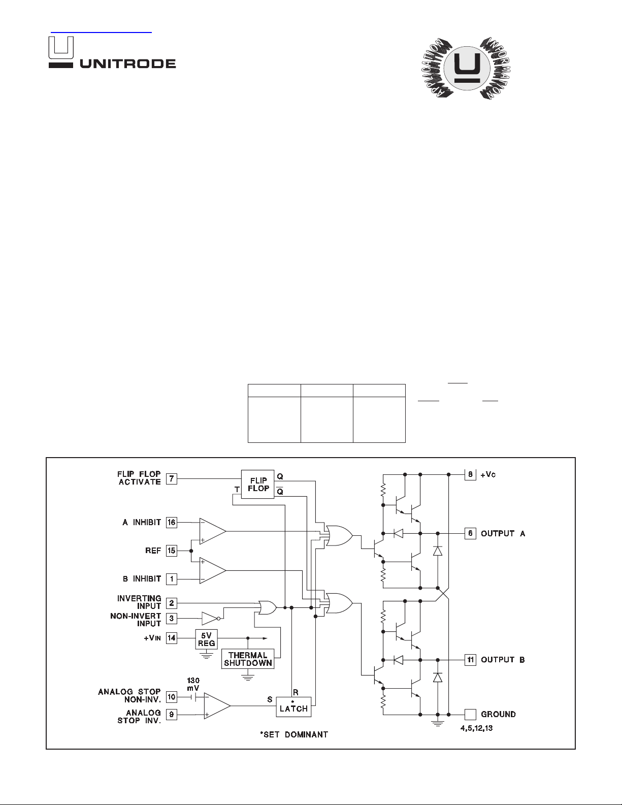
BLOCK DIAGRAM
DESCRIPTION
The UC1706 family of output drivers are made with a high-speed
Schottky process to interface between low-level control functions and
high-power switching devices - particularly power MOSFET's. These devices implement three generalized functions as outlined below.
First: They accept a single-ended, low-current digital input of either polarity and process it to activate a pair of high-current, totem pole outputs
which can source or sink up to 1.5A each.
Second: They provide an optional single-ended to push-pull conversion
through the use of an internal flip-flop driven by double-pulsesuppression logic. With the flip-flop disabled, the outputs work in parallel
for 3.0A capability.
Third: Protection functions are also included for pulse-by-pulse current
limiting, automatic deadband control, and thermal shutdown.
These devices are available in a two-watt plastic “bat-wing” DIP for operation over a 0°C to 70°C temperature range and, with reduced power,
in a hermetically sealed cerdip for -55°C to +125°C operation. Also available in surface mount Q and L packages.
TRUTH TABLE
INV N.I OUT
H
L
H
L
H
H
L
L
L
H
L
L
OUT = INV and N.I.
OUT
= INV or N.I.
10/98
ABSOLUTE MAXIMUM RATINGS
....................................... N--Pkg ............ J--Pkg
Supply Voltage, VIN .........................40V..................40V
Collector Supply Voltage, VC ..................40V..................40V
Output Current (Each Output, Source or Sink)
Steady--State..........................±500mA ..............±500mA
Peak Transient..........................±1.5A ................±1.0A
Capacitive Discharge Energy .............. 20mJ................. 15mJ
Digital Inputs ..............................5.5V .................5.5V
Analog Stop Inputs......................... VIN.................. VIN
Power Dissipation at TA = 25°C (See Note) .......2W ..................1W
Power Dissipation at T (Leads/Case) = 25°C......5W...................2
(See Note)
Operating Temperature Range ......................--55°C to +125°C
Storage Temperature Range........................--65°C to +150°C
Lead Temperature (Soldering, 10 Seconds) ................300°C
Note: All voltages are with respect to the four ground pins which must be connected
together.All currents are positive into, negative out of the specified trerminal. Consult
Packaging sections of the Databook for thermal limitations and considerations of package.
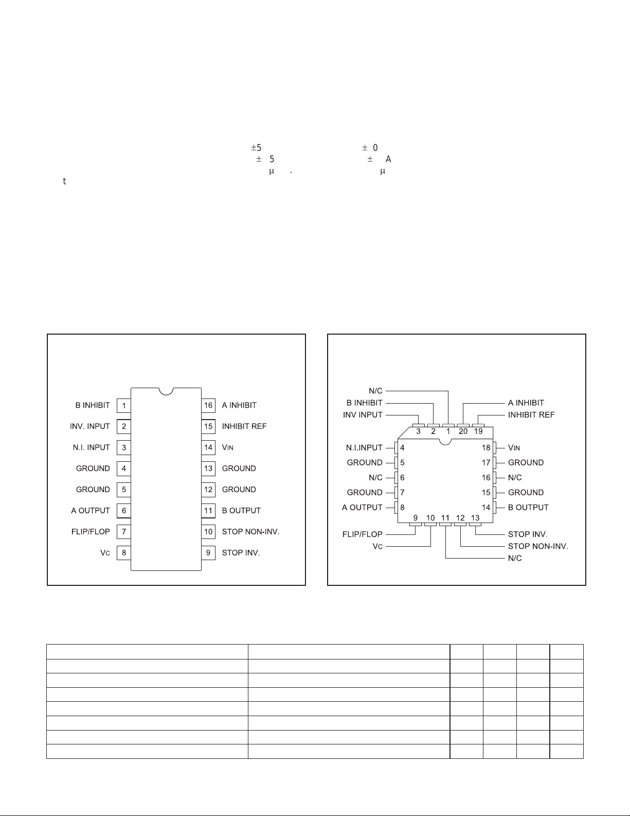
CONNECTION DIAGRAMS
UC1706
UC2706
UC3706
DIL-16, SOIC-16 (TOP VIEW)
JorNPackage,DWPackage
Note: All four ground pins must be connected to a common
ground.
PLCC-20, LCC-20 (TOP VIEW)
Q, L Packages
ELECTRICAL CHARACTERISTICS: Unless otherwise stated, these specifications apply for TA = –55°C to +125°C for
the UC1706, –25°C to +85°C for the UC2706 and 0°C to +70°C for the UC3706; VIN =VC= 20V. TA =TJ.
PARAMETERS TEST CONDITIONS MIN TYP MAX UNITS
IN Supply Current VIN = 40V 8 10 mA
V
VC Supply Current VC = 40V, Outputs Low 4 5 mA
VC Leakage Current VIN =0,VC= 30V, No Load .05 0.1 mA
Digital Input Low Level 0.8 V
Digital Input High Level 2.2 V
Input Current V
Input Leakage V
I = 0 –0.6 –1.0 mA
I = 5V .05 0.1 mA
2
 Loading...