

Page 1
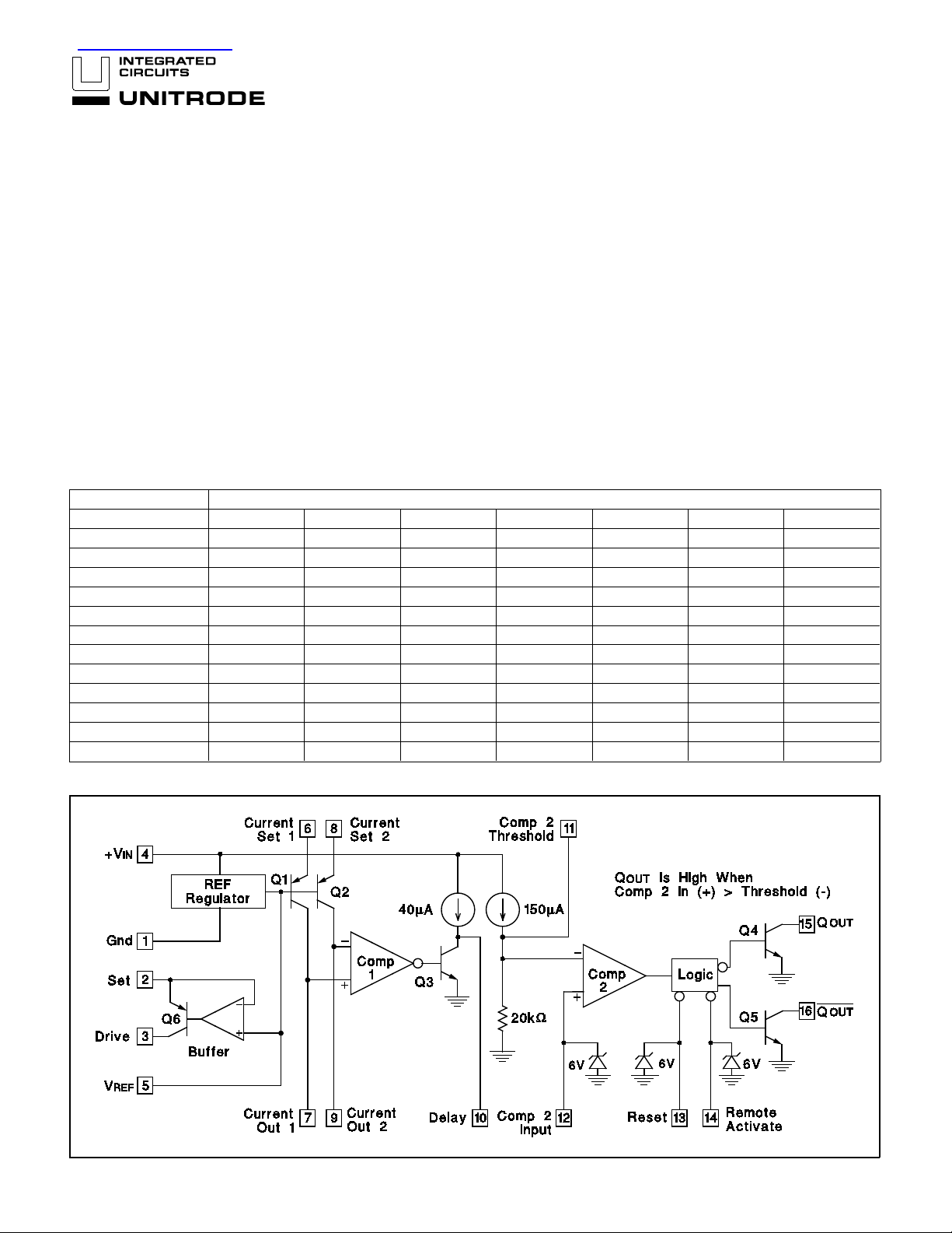
This integrated circuit contains a complete signal conditioning system to interface low-level variable impedance transducers to a
digital system. A pair of matched, temperature-compensated current sources are p rovided for balanced transducer excitation followed by a precision, high-gain comparator. The output of this
comparator can be delayed by a user-selectable duration, after
which a second comparator will switch complementary outputs
separately activated for diagnostic operation and has an optional
latch with external rese t capabil ity. An added feature is a high current power source useful as a heater driver in differential temperature sensing applications. The UC3704 is designed for 0°C to
+70°C environments.
查询UC3704供应商
Bridge Transduc er Swit ch
UC3704
FEATURES
• Dual Matched Current Sources
• High-gain Differential Sensing Circuit
• Wide Common-mode Input Capability
• Complementary Digital Open-collector
Outputs
• Externally Programm a ble Time Delay
• Optional Output Latch with Reset
• Built-in Diagnostic Activation
• Wide Supply Voltage Range
• High Current Heater Power Source Driver
DESCRIPTI ON
UC3704 COMPATIBLE SE NSO RS
SENSOR TYPE ACTIVATION SOURCE
Temperature Pressure Force Position Displacement Velocity Shock
Thermistor X X
Sensistor X X
Thermocouple X
Semiconductor X X X
Photo Voltaic X X X
Photo Resistive X X X
Strain Gag e XXXXXX
Piezoelectric X X X X X
Magneto Resistive X X
Inductive XXXX
Hall Effect X X
Capacitive X
BLOCK DIAGRA M
6/93
Page 2
UC3704
ABSOLUTE MAXI MUM RATING S
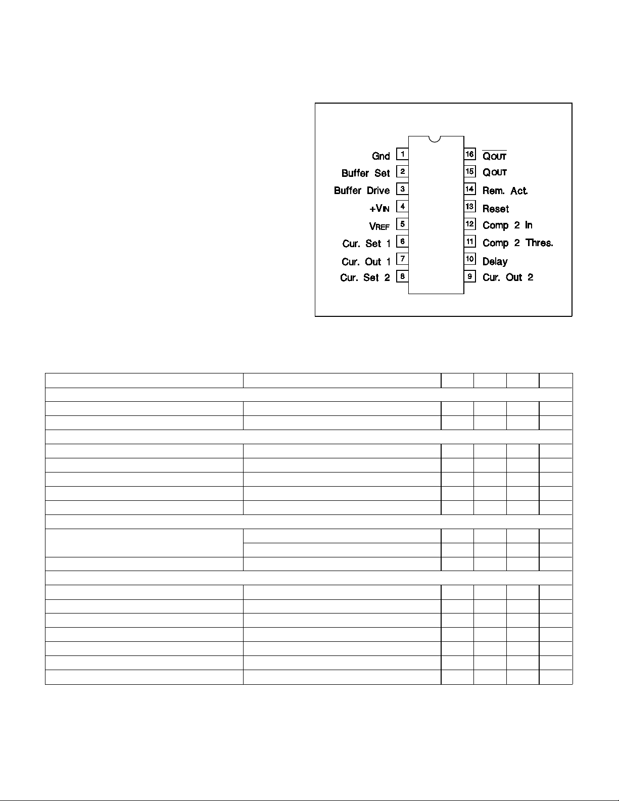
CONNECTION DIAGRAM
Supply Voltage ( +V IN). . . . . . . . . . . . . . . . . . . . . . . . . . . . . . 40 V
Output Current (each output) . . . . . . . . . . . . . . . . . . . . . . 50 mA
Buffer Power So urce Current. . . . . . . . . . . . . . . . . . . . . 200mA
Compara to r 1 Inputs. . . . . . . . . . . . . . . . . . . . . . . -0.5V to V
REF
DIL-16 (TOP VI EW)
J or N Package
Compara to r 2 Inputs. . . . . . . . . . . . . . . . . . . . . . . . . . . 0 to 5.5V
Remote Activa tion and Reset Inpu ts . . . . . . . . . . . . . . 0 to 5.5V
Power Dissipation at T
A = 25°C . . . . . . . . . . . . . . . . . . 1000mW
Operating Junct ion Te mp era tu re . . . . . . . . . . . -55°C to +150°C
Storage Temperature Range . . . . . . . . . . . . . . -65°C to +150°C
Lead Tempera ture (Solder ing, 10 Seconds) . . . . . . . . . +3 00°C
Note: Unless otherw ise specified, all volta ges are with respect
to ground (Pin 1).
Currents are positiv e into , negat ive out of th e specified
terminal.
Consult Packag in g sect ion of Dat abo ok f or therm al
imitations and con sider at ions of package.
ELECTRICAL CHARACTERISTICS:
Unless otherwise state d, these spe cifica tion s apply for TA = 0°C to +70°C for the
UC3704: V
IH = 15V, TA =TJ.
PARAMETERS TEST CONDITION S MIN TYP MAX UNITS
Power Inputs
Supply Voltage Range 4.2 36 V
Supply Current V
Reference Sec tion ( w ith respect to V
REF Value |VIN - VREF|TJ = 25°C 2.1 2.2 2.3 V
V
V
REF Temperatur e Coeff icie nt Note 1 -1 -2 -3 mV/°C
IN)
Line Regulatio n ∆V
Load Regulation ∆I
Short Circuit Current V
IN = 36V 5 10 mA
IN = 4.2 to 25V 2 10 mV
O = 0 to 4mA 2 10 mV
IN = 36V, VREF = VIN or Ground
±
25 mA
Current Source ( Q1 and Q 2)
Output Cur rent (Note 2) Current Set = 10µA-9-9.5-10µA
Current Set = 200 µA -180 -195 -200 µA
Output Offset Current R
E6 = RE8 = 20kΩ 0
±
1 µA
Comparator One
Input Offs et Vo lta ge
±
±
1
4mV
Input Bias Cur rent -100 -300 nA
Input Offs et Cu rr ent
CMRR V
Voltage gain R
CM = 0 to 12V 60 70 dB
L>150kΩ 70 85 dB
±
60 nA
Delay Current Source 34 40 52 µA
Output Rise Time Overdrive = 10mV, C
D = 15pF, TJ = 20° C 2 V/µs
2
Page 3

UC3704
ELECTRICAL CHARACTERIST ICS :
PARAMETER TEST CONDITIONS M IN TYP MAX UNITS
Comparator Two (Q
Threshold Voltage 2.2 3.0 3.8 V
Threshold Resistanc e To Ground 14 20 24 kΩ
Input Bias Cur rent V
Remote Activat e Cur ren t Pin 14 = 0V 0.2 0.5 mA
Reset Current Pin 13 = 0V 0.2 0.5 mA
Remote Activat e Thr esh old T
Reset Threshold T
Output Saturation I
Output Lea kage V
Output Resp onse Comp. O verdrive = 1V
Buffer
Set Voltage (V
Drive Current T
OUT
and QOUT)
IN -VS)TJ = 25°C, IS = 100mA 1.9 2.1 2.3 V
Unless otherw ise stat ed, these sp ecif icat io ns apply for TA = 0°C to +70°C for the
UC3704: V
IN (Pin 12) = 5V 1 3 µA
A = 25°C 0.8 1.2 V
A = 25°C 0.8 1.2 V
OUT = 16mA 0.2 0.5 V
OUT = 50mA 0.7 2.0 V
I
OUT = 40V 0.2 10 µA
R
L
J = 25°C, RS = 200Ω, VD = 0V 90 100 120 mA
IH = 15V, TA =TJ.
= 5k to VIN
Turn- on 0.4 µs
Turn- of f 1.0 µs
Note 1: Parameter guar anteed by design, not tested in productio n.
IN
−
V
REF
−
V
Note 2: Collector out put cur re nt =
V
BE
R
E
≈
1.5
R
V
E
APPLICATIONS INFORMATION
Sensor Section
The input portion of the UC3704 provides both excitation
and sensing for a low-level, variable impedance
transducer. This circuitry consists of a pair of highly
matched PNP transistor s biased for operation as constant
current sources followed by a hi gh gain precision comparator.
The reference voltage at the bases of the PNP transistors
has a TC to offset the base-emitter voltage variation of
these transistors resulting in a constant voltage across
the external emitter resistors and correspondingly constant collector currents for balancing, offsetting, or to provide unique temperature characterist ic.
With the PNP transistor’s optimum current ranging from
10 to 200µA, and the common-mode input voltage of the
comparator usable from ground to (V
range of transducer impedance levels is possible.
The sensor comparator has a current source pull-up at
the output so that an external capacitor from this point to
IN - 3V), a wide
ground can be used to provide a programmable delay before reaching the second comparator’s threshold. The
low-impedance on-state of Comp 1’s output provides
quick reset of this capacitor. This programmable delay
function is useful for providing transi ent protection by requiring that Comp 1 remain activated for a finite period of
time before Comp 2 triggers. Another application is in
counting repe titive pulses where a missing pulse will allow Comp 1’s output to rise to Comp 2’s threshold. This
time delay function is:
Delay
=
Delay
Threshold
Current
X
C
D
≈ 175
ms
⁄
µ
F
Comp
2
If hysteresis is desired for Comparator 1, it may be accommodated by applyin g positive feedback from the delay ter minal to the n on-inverting i nput on Pin 7. This will
aid in provid ing oscillation-free transitions for very slowly
changing inputs.
3
Page 4

APPLICATIONS INFORMATION (cont.)
Output Section
The output portion of the UC3704 is basically a second
comparator with complimentary, open-collector outputs.
This comparator has a built-in, ground-referenced threshold implemented with a high-impedance current source
and resistor so that it may be easil y overridden with an
external voltage source if desired. Comp 2’s input transistors are NPN types which require at least 1V of common-mode voltage for accurate operation and should not
see a differentia l input voltage greater than 6V.
For diagnostic or latching purposes, the output logic is
equipped with a Remote Activate and Reset function.
These pins have internal pull-ups and are only active
when pulled low below a threshold of approximately 1V . A
low signal at the Remote Activate Pin causes the outputs
to change state in exactly the same manner as if Comp
2’s input is raised above the threshold on Pin 11. If Pin
16 is connected to Pi n 14, positive feedback results and
the outputs will latch once triggered by Comp 2’s input.
UC3704
Pulling the Reset terminal low overrides the Remote Activate Pin releasing the latch.
Reference Buffer
This circuit is designed to provide up to 100mA to drive a
high current external PNP transistor useful for powering
a heater for differential temperature measurements. Care
must be taken that power dissipation in Q6 does not
cause excessive thermal gradients which will degrade
the accuracy of the sensing circuitry.
Using a heating element a ttached to a temperature sensitive resis tor, RS1, in one leg o f the inp ut bridge i mplements a flow sensor for either gasses or liquids. As long
as there is flow, heat from the element is carried away
and the sensor vol tage remains below threshol d. Using
an identical sensor, RS2, without a heater to establish
this threshold compensates for the ambie nt temperature
of the flow.
TYPICAL APPL ICATION FOR MONITORING LIQUID OR GAS FLOW
UNITRODE INTEGRATED CIRCUITS
7 CONTINENTAL BLVD.•• MERRIMACK, NH 03054
TEL. (603) 424-2410 •• FAX (603) 424-3460
4
Page 5

IMPORTANT NOTICE
T exas Instruments and its subsidiaries (TI) reserve the right to make changes to their products or to discontinue
any product or service without notice, and advise customers to obtain the latest version of relevant information
to verify, before placing orders, that information being relied on is current and complete. All products are sold
subject to the terms and conditions of sale supplied at the time of order acknowledgement, including those
pertaining to warranty, patent infringement, and limitation of liability.
TI warrants performance of its semiconductor products to the specifications applicable at the time of sale in
accordance with TI’s standard warranty. Testing and other quality control techniques are utilized to the extent
TI deems necessary to support this warranty . Specific testing of all parameters of each device is not necessarily
performed, except those mandated by government requirements.
CERTAIN APPLICATIONS USING SEMICONDUCTOR PRODUCTS MAY INVOLVE POTENTIAL RISKS OF
DEATH, PERSONAL INJURY, OR SEVERE PROPERTY OR ENVIRONMENTAL DAMAGE (“CRITICAL
APPLICATIONS”). TI SEMICONDUCTOR PRODUCTS ARE NOT DESIGNED, AUTHORIZED, OR
WARRANTED TO BE SUITABLE FOR USE IN LIFE-SUPPORT DEVICES OR SYSTEMS OR OTHER
CRITICAL APPLICA TIONS. INCLUSION OF TI PRODUCTS IN SUCH APPLICATIONS IS UNDERST OOD TO
BE FULLY AT THE CUSTOMER’S RISK.
In order to minimize risks associated with the customer’s applications, adequate design and operating
safeguards must be provided by the customer to minimize inherent or procedural hazards.
TI assumes no liability for applications assistance or customer product design. TI does not warrant or represent
that any license, either express or implied, is granted under any patent right, copyright, mask work right, or other
intellectual property right of TI covering or relating to any combination, machine, or process in which such
semiconductor products or services might be or are used. TI’s publication of information regarding any third
party’s products or services does not constitute TI’s approval, warranty or endorsement thereof.
Copyright 1999, Texas Instruments Incorporated
 Loading...