

查询UC1633供应商
Phase Locked Frequency Controller
UC1633
UC2633
UC3633
FEATURES
• Precision Phase Locked Frequency
Control System
• Crystal Oscillator
• Programmable Reference Frequency
Dividers
• Phase Detector with Absolute Frequency
Steering
• Digital Lock Indicator
• Double Edge Option on the Frequency
Feedback Sensing Amplifier
• Two High Current Op-Amps
• 5V Reference Output
DESCRIPTION
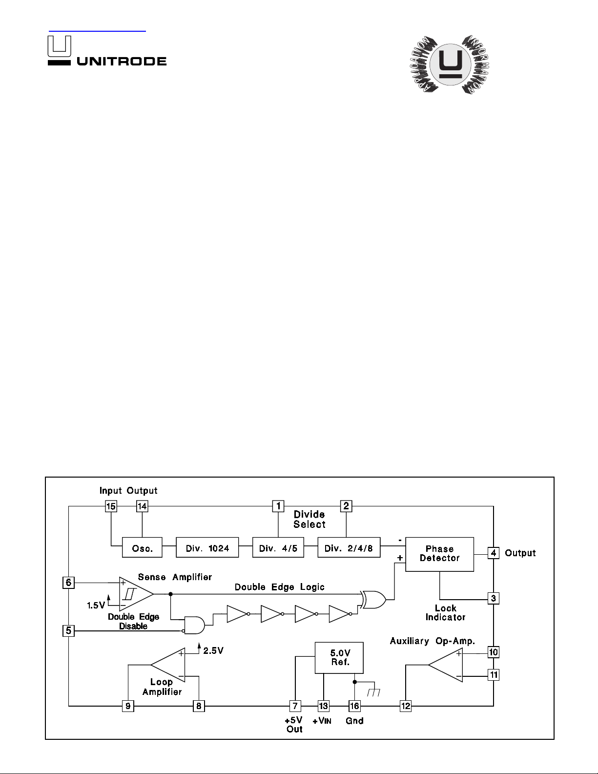
The UC1633 family of integrated circuits was designed for use in phase
locked frequency control loops. While optimized for precision speed
control of DC m ot ors, t hes e devices ar e u niversa l en ough for most applications that require phase locked control. A precise reference frequency c an be generated us ing the device’s high frequency oscillator
and programma ble frequency dividers. The oscillator operates using a
broad range of crystals, or, can function as a buffer stage to an external
frequency source.
The phase detector on these integrated circuits compares the reference freque ncy with a f requenc y/phase feedback signal. In the case of
a motor, feedback is obtained at a hall ou tput of ot her speed detection
device. This signal is buffered by a sense ampilfier that squares up the
signal as it goes into the digital phase detector. The phase detector responds propor tionally to the phase error between the reference and the
sense amplifier output. This phase detector includes absolute frequency steering to provide maximum drive signals when any frequency
error exists. This feature allows optimum start-up and lock times to be
realized.
Two op-amps are included that can be configured to provide necessary
loop filtering. The outputs of the op-amps will source or sink in excess
of 16mA, so they can provide a low impedence control signal to driving
circuits.
BLOCK DIAGRAM
Additional featur es i nc l ud e a do uble edge option on the sense amplifier
that can be use d to double the loop reference frequency for increased
loop bandwidths. A digital lock signal is provided that indicates when
there is zero fr equen cy erro r, and a 5V reference output allows DC operating levels to be accurately set.
4/97
1
ABSOLUTE MAXIMUM RATINGS
Input Supply Voltage (+VIN) . . . . . . . . . . . . . . . . . . . . . . . . +20V
Reference Output Current . . . . . . . . . . . . . . . . . . . . . . . . -30mA
Op-Amp Output Currents . . . . . . . . . . . . . . . . . . . . . . . . ±30mA
Op-Amp Input Voltages . . . . . . . . . . . . . . . . . . . . . -.3V to +20V
Phase Detector Output Current . . . . . . . . . . . . . . . . . . . ±10mA
Lock Indicator Output Current . . . . . . . . . . . . . . . . . . . . +15mA
Lock Indicator Output Voltage . . . . . . . . . . . . . . . . . . . . . . +20V
Divide Select Input Voltages . . . . . . . . . . . . . . . . . -.3V to +10V
Double Edge Disable Input Voltage . . . . . . . . . . . . -.3V to +10V
Oscillator Input Voltage . . . . . . . . . . . . . . . . . . . . . . -.3V to +5V
Sense Amplifier Input Voltage . . . . . . . . . . . . . . . . .3V to +20V
Power Dissipation at TA = 25°C (Note 2 . . . . . . . . . . . 1000mW
Power dissipation at TC = 25°C (Note 2) . . . . . . . . . . . 2000mW
Operating Junction Temperature . . . . . . . . . . . -55°C to +150°C
Storage Temperature . . . . . . . . . . . . . . . . . . . . -65°C to +150°C
Lead Temperature (Soldering, 10 Seconds) . . . . . . . . . . 300°C
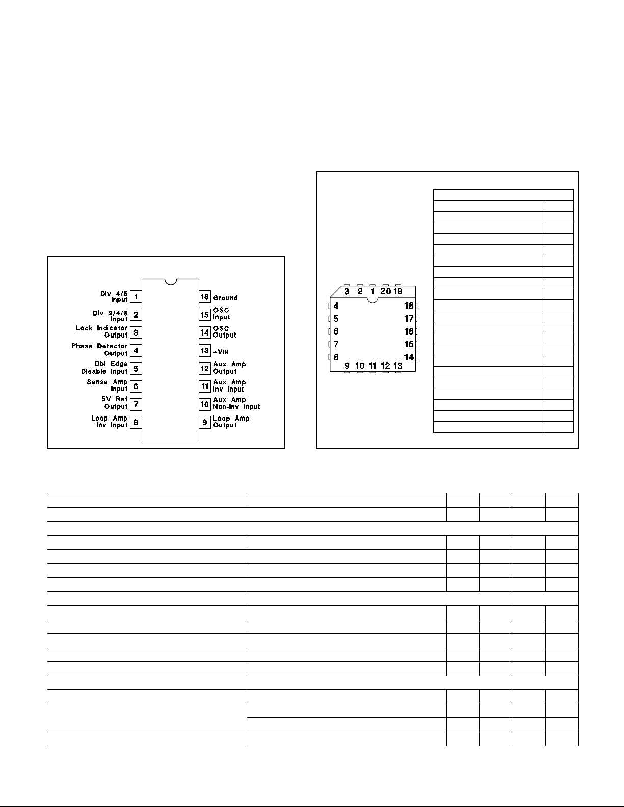
DIL-16 (TOP VIEW)
J or N Package
UC1633
UC2633
UC3633
Note1: V oltages are referenced to ground, (Pin 16). Currents
are positive into, negative out of, the specified terminals.
Note 2: Consult Packaging Section of Databook for thermal limitations and considerations of package.
CONNECTION DIAGRAMS
PLCC-20 (T OP VIEW)
Q Package
PACKAGE PIN FUNCTION
FUNCTION PIN
N/C
Div 4/5 Input
Div 2/4/8 Input
Lock Indicator Output
Phase Detector Output
N/C
Dbl Edge Disable Input
Sense Amp Input
5V Ref Output
Loop Amp Inv Input
N/C
Loop Amp Output
Aux Amp Non-Inv Input
Aux Amp Inv Input
Aux Amp Output
N/C
+V
IN
OSC Output
OSC Input
Ground
1
2
3
4
5
6
7
8
9
10
11
12
13
14
15
16
17
18
19
20
ELECTRICAL CHARACTERISTICS:
(Unless otherwise stated, these specifications apply for TA = 0°C to +70°C for the
UC3633, -25°C to +85°C for the UC2633, -55°C to +125°C for the UC1633, +VIN =
12V; TA=TJ.)
PARAMETER TEST CONDITIONS MIN. TYP. MAX. UNITS
Supply Current +VIN = 15V 20 28 mA
Reference
Output Voltage (V
Load Regulation I
Line Regulation +V
Short Circuit Current V
) 4.75 5.0 5.25 V
REF
= 0V to 7mA 5.0 20 mV
OUT
= 8V to 15V 2.0 20 mV
IN
= 0V 12 30 mA
OUT
Oscillator
DC Voltage Gain Oscillator Input to Oscillator Output 12 16 20 dB
Input DC Level (V
Input Impedance (Note 3) V
) Oscillator Input Pin Open, TJ = 25°C 1.15 1.3 1.45 V
IB
= VIB ±0.5V, TJ = 25°C 1.3 1.6 1.9 k
IN
Output DC Level Oscillator Input Pin Open, TJ = 25°C 1.2 1.4 1.6 V
Maximum Operating Frequency 10 MHz
Dividers
Maximum Input Frequency Input = 1VPP at Oscillator Input 10 MHz
Div. 4/5 Input Current Input = 5V (Div. by 4) 150 500
Input = 0V (Div. by 5) -5.0 0.0 5.0
Div. 4/5 Threshold 0.5 1.6 2.2 V
Note 3: These impedence levels will vary with TJ at about 1700ppm/°C
Ω
A
µ
A
µ
2

UC1633
UC2633
UC3633
ELECTRICAL
CHARACTERISTICS (cont.):
(Unless otherwise stated, these specifications apply for TA = 0°C to +70°C for t he UC3 633,
-25°C to +85°C for the UC2633, -55°C to +125°C for the UC1633, +VIN = 12V; TA=TJ.)
PARAMETER TEST CONDITIONS MIN. TYP. MAX. UNITS
Dividers (cont.)
Div. 2/4/8 Input Curre nt Input = 5V (Div. by 8) 150 500
Input = 0V (Div. by 2) -500 -150
Div. 2/4/8 Open Circui t Voltage Input Current = 0µA (Div. by 4) 1.5 2.5 3.5 V
Div. by 2 Threshold 0.20 0.8 V
Div. by 4 Threshold 1.5 3.5 V
Div. by 8 Threshold Volts Below V
REF
0.20 0.8 V
Sense Amplifier
Threshold Voltage Percent of V
REF
27 30 33 %
Threshold Hysteresis 10 mV
Input Bias Current Input = 1.5V -1.0 -0.2
Double Edge Disable Input
Input Current Input = 5V (Disabled) 150 500
Input = 0V (Enabled) -5.0 0.0 5.0
Threshold Voltage 0.5 1.6 2.2 v
Phase Detector
High Output Level Positive Phase/Freq. Error, Volts Below V
REF
0.2 0.5 V
Low Output Level Negative Phase/Freq. Error 0.2 0.5 V
Mid Output Level Zero Phase/Freq. Error, Percen t of V
High Level Maximum Source Current V
Low Level Maximum Sink Current V
Mid Level Outpu t Im pe da nc e (N ot e 3) I
= 4.3V 2.0 8.0 mA
OUT
= 0.7V 2.0 5.0 mA
OUT
= -200 to +200µA, TJ = 25°C 4.5 6.0 7.5 k
OUT
REF
47 50 53 %
Lock Indicator Output
Saturation Voltage Freq. Error, I
Leakage Current Zero Freq. Error, V
= 5mA 0.3 0.45 V
OUT
= 15V 0.1 1.0
OUT
Loop Amplifier
NON INV. Reference Voltage Percent of V
REF
47 50 53 %
Input Bias Current Input = 2.5V -0.8 -0.2
AVOL 60 75 dB
PSRR +V
Short Circuit Current Source, V
= 8V to 15V 70 100 dB
IN
= 0V 16 35 mA
OUT
Sink, V
= 5V 16 30 mA
OUT
Auxiliary Op-Amp
Input Offset Voltage V
= 2.5V 8 mV
CM
Input Bias Current VCM = 2.5V -0.8 -0.2
Input Offset Current V
= 2.5V .01 0.1
CM
AVOL 70 120 dB
PSRR +V
= 8V to 15V 70 100 dB
IN
CMRR VCM = 0V to 10V 70 100 dB
Short Circuit Current Source, V
Sink, V
= 0V 16 35 mA
OUT
= 5V 16 30 mA
OUT
Note 3: These impedence levels will vary with TJ at about 1700pp m/°C
A
µ
A
µ
A
µ
A
µ
A
µ
Ω
A
µ
A
µ
A
µ
A
µ
3
 Loading...