

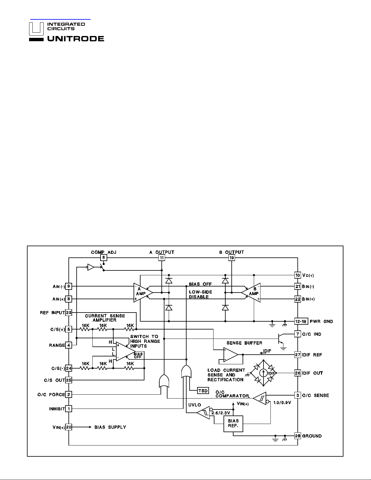
The UC3178 ful l-bridge power amplifier, rated for continuous output current
of 0.45 Amperes, i s intended for use in demanding servo applications. This
device includes a preci sion current sense amplifier that senses load current
with a single resistor in series with the load. The UC3178 is optimized to con sume a minimum of supply current , and is designed to operate in both 5V
and 12V systems. The power output stages have a l ow saturation voltage
and are protected with current limiting and thermal shutdown. When inhibited,
the device will draw less than 1.5mA of total supply current.
Auxiliary functions on this device include a load current sensing and rectification function that can be configured with the device’s over-current comparator
to provide tight control on the maximum commanded load current. The closed
loop transconductance of the configured power amplifier can be switched between a high and l ow ran ge wi th a single logic input. The 4:1 change in gain
can be used to extend the dynamic range of the servo loop. Bandwidth variations that would otherwise result with the gain change can be controlled w ith
a compensation adjust pin.
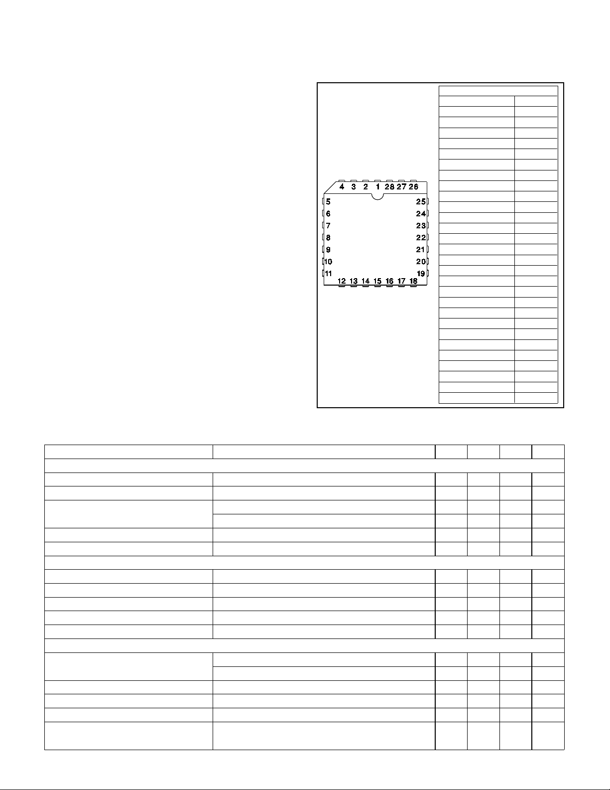
This device is packaged a power PLCC, "QP" package which maintains a
standard 28-pin outline, but with 7 pins along one edge directly tied to the die
substrate for improved thermal performance.
查询UC3178供应商
Full Bridge Power Amplifier
UC3178
FEATURES
• Precision Current Control
•±450mA Load Current
• 1.2V Typical Total Vsat at
450mA
• Programmable Over-Current
Control
• Range Control for 4:1 Gain
Change
• Compensation Adjust Pin for
Range Bandwidth Control
• Inhibit Input and UVLO
• 3V to 15V Operation
• 12mA Quiescent Supply
Current
BLOCK DIAGRAM
DESCRIPTION
5/93
UDG-92010
UC3178
Unless otherwise stat ed spe cifica tion s hold for TA = 0°C to 70°C, VC(+) = VIN(+) =
12V, REF Input = VIN(+)/2, O/C Inpu t & Inhibit Input = 0V.
ABSOLUTE MAXIMUM RATINGS
Input Supply Vo ltage, (VIN(+), VC(+) ). . . . . . . . . . . . . . . . . . 20V
O/C Sense, Log ic Input s, and REF Input
Maximum forced voltage. . . . . . . . . . . . . . . . . -0.3V to 10V
Maximum forced current . . . . . . . . . . . . . . . . . . . . . . ±10mA
A & B Amplifier Inputs . . . . . . . . . . . . . -0.3V to (V
IN(+) + 1.0V)
O/C Indicate O pen Collector Output Voltage. . . . . . . . . . . . 20V
A and B Output Cur ren ts(co nt in uous )
Source . . . . . . . . . . . . . . . . . . . . . . . . . . . . Internally Limited
Sink . . . . . . . . . . . . . . . . . . . . . . . . . . . . . . . . . . . . . . . . 0.6A
Output Diode Cur re nt (pulse d)* . . . . . . . . . . . . . . . . . . . . . 0.5A
O/C Ind Output Current (c ont inuous) . . . . . . . . . . . . . . . . 20mA
Operating Jun ctio n Tem per atur e. . . . . . . . . . . . . . . . . . +150°C
Storage Temperature. . . . . . . . . . . . . . . . . . . -65°C to +150 °C
*Notes: Unless other wise indicat ed , voltag es are refer enc ed to
ground and curre nts are posit ive into , negat ive out of , the specified terminals, "Pu lsed" is defin ed as a less tha n 10% dut y cycle pulse with a maximum dura tion of 500
µs.
THERMAL DATA
QP package: (see pac kaging sect ion of UICC data book for more
details on therm al perfor m ance )
Thermal Resistance Junction to Leads, θjl . . . . . . . . 15°C/W
Thermal Resistance Junction to Ambient, θja . . . 30-40°C/W
Note: The above numbers for θjl are maximums for the limiti ng
thermal resist anc e of the packa ge in a standa rd moun ting configuration . The
thermal perfor ma nce of t he dev ice/ pc- boar d sy stem . All of the
above numbers assume no ambient airflow.
θ
ja numbers are meant to be guideline s for the
CONNECTION DIAG RAM
PLCC - 28 (Top View)
QP Package
PACKAGE PIN FUNCTION
FUNCTION PIN
Inhibit 1
O/C Force 2
O/C Sen se 3
Range 4
C/S(+) 5
Comp Adj 6
O/C Ind 7
IN(+) 8
A
IN(-) 9
A
V
C(+) Supply 10
A Output 11
Pwr Gnd 12
Pwr Gnd 13
Pwr Gnd 14
Pwr Gnd 15
Pwr Gnd 16
Pwr Gnd 17
Pwr Gnd 18
B Output 19
IN(+) 20
V
IN(-) 21
B
B
IN(+) 22
REF Input 23
C/S(+) 24
C/S Out 25
IDIF Out 26
IDIF REF 27
Ground 28
ELECTRICAL CHARACTERIST ICS :
PARAMETER TEST CONDITIONS MIN TYP MAX UNITS
Input S u p pl y
V
IN (+)Supply Cur rent 12 16 mA
VC(+) Supply Current IOUT = OA 1.2 2.0 mA
Total Supply Current Supplies = 5V,I
Supplies = 12V,I
V
IN(+) UVLO Threshold low to high 2.6 2.8 V
UVLO Threshold Hysterisis 300 mV
Over-Cur ren t (O/C) Comp ara tor
Input Bias Curr ent V input = 0.8V -1.0 -.01 µA
Thresholds low to high 0.97 1.0 1.03 V
Threshold Hys terisis 85 100 115 mV
O/C IND Vs at I
O/C IND Leakage V
OUT = 5mA, V input low 0.2 0.45 V
OUT = 20V 5.0 µA
Power Amplifiers A and B
Input Off set Voltage A Amplifier, V
B Amplifier, V
Input Bias Current V
CMRR V
CM = 6V -500 -50 µΑ
CM = 0.5 to 13V, Supplies = 15V 70 90 dB
PSRR VIN(+) = 4 to 15V, VCM = 1.5V 70 90 dB
Large Signal Volta ge G ain Supplies = 12V, V
to V
OUT = 10.5V, IOUT = -300mA 3.0 15.0 V/mV
OUT = OA 12 16 mA
OUT = OA 13 18 mA
CM = 6V 4.0 mV
CM = 6V 12.0 mV
OUT = 1V, IOUT = 3 00mA
2
 Loading...