

查询UC3176QP供应商
Full Bridge Power Amplifier
FEATURES DESCRIPTION
• Dual Power Operational Amplifiers
•±2A Output Current Guaranteed
• Precision Current Sense Amplifier
• Two Supply Monitoring Inputs
• Parking Function and Under-Voltage
Lockout
• Safe Operating Area Protect ion
• 3V to 35V Operation
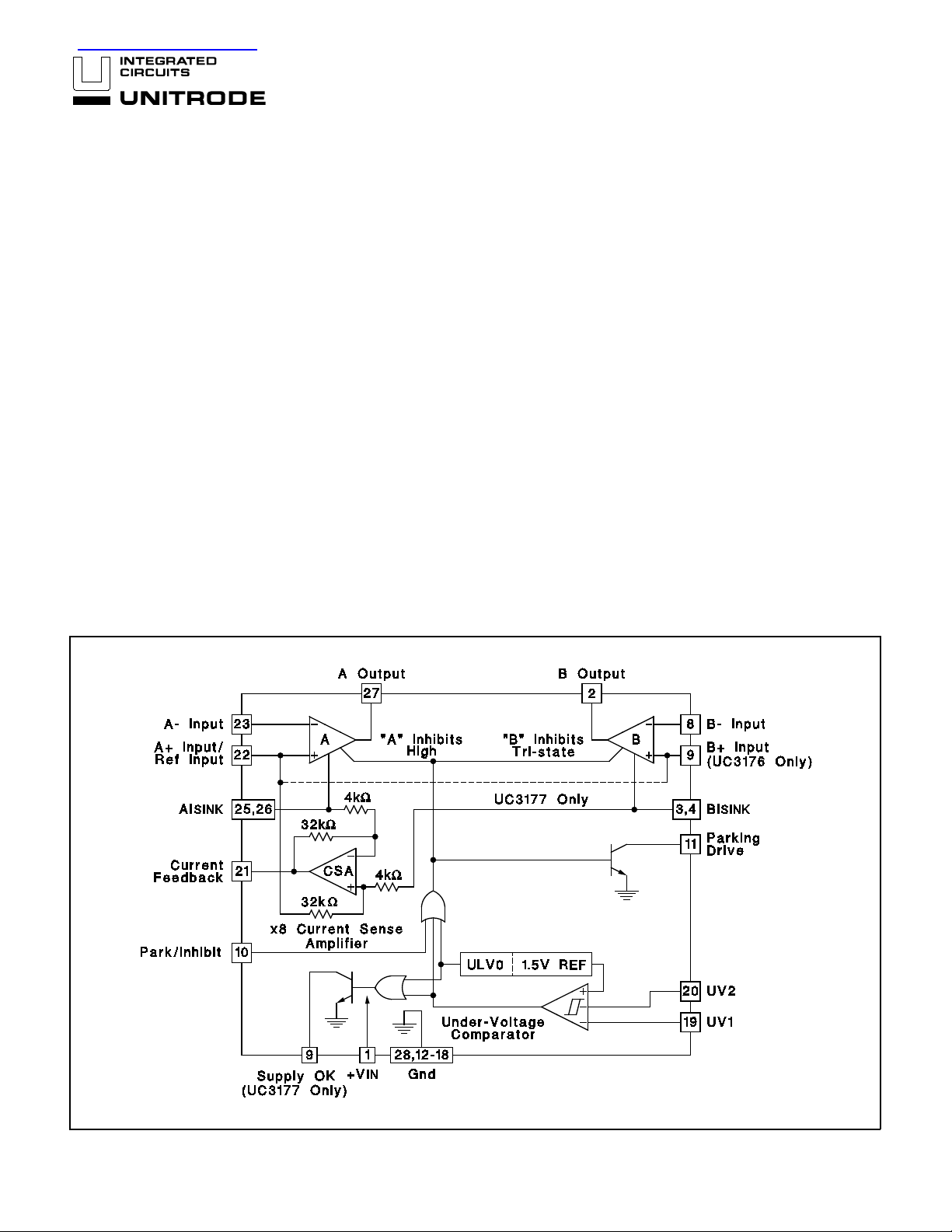
The UC3176/7 family of full bridge power amplifiers is rated for a continuous output current of 2A. Intended for use in dem anding servo applications
such as disk head positioning, the onboard current sense amplifier can be
used to obtain precision control of load current, or where voltage mode
drive is required, a standard voltage feedback scheme can be used. Output stage protection includes foldback current l imiting and thermal shutdown, resulting in a very rugged device.
Auxiliary functions on this device i nclude a dual in put under-voltage comparator that can be programmed to respond to low voltage conditions on
two independent supplies. In response to an under-voltage condition the
power Op-Amps are inhibited and a high current, 100mA, open collector
drive output is activated. A separate Park/Inhibit command input.
The devices a re operational over a 3V to 35V supply range. Internal under-voltage lockout p rovides predictable power-up and power-down characteristics.
UC3176
UC3177
BLOCK DIAGRAM
10/94
ABSOLUTE MAXIMUM RATINGS (Note 1)
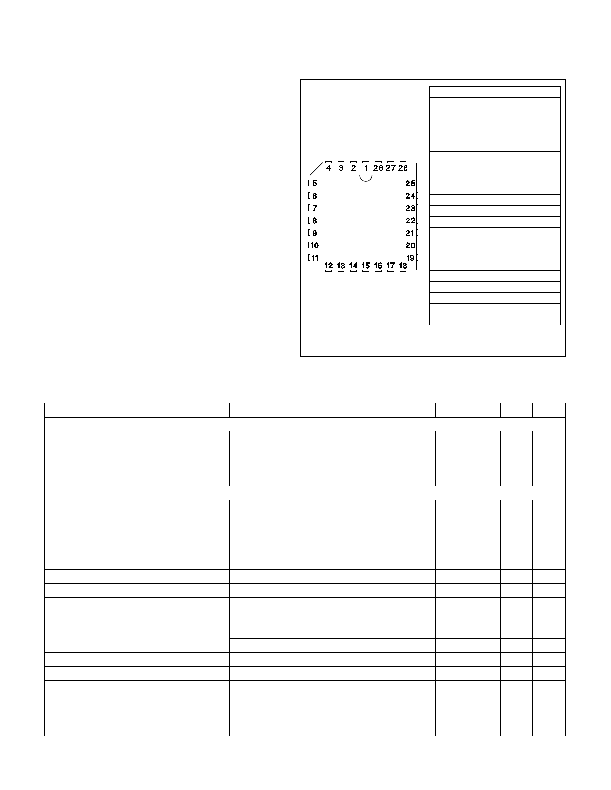
*Pin 9: UC3176, B+ Input
UC3177, Supply OK
Input Supply voltage, (+VIN). . . . . . . . . . . . . . . . . . . . . . . 40V
Park/Inhibit, UV1 and UV2 inputs (ze ner clamp ed)
Maximum forced voltage . . . . . . . . . . . . . . . . -0.3V to 10V
Maximum forced curr ent. . . . . . . . . . . . . . . . . . . . . ±10mA
Ot h er Inpu t Vo l tages. . . . . . . . . . . . . . . . . . . . . -0.3V t o +V
AlSINK and BlSINK Voltages. . . . . . . . . . . . . . . . . . -0.3V to 6V
Open Collector Out put Voltages. . . . . . . . . . . . . . . . . . . . 40V
A and B Output Curren ts (Continuo us)
Source . . . . . . . . . . . . . . . . . . . . . . . . . . Internally Limited
Sink. . . . . . . . . . . . . . . . . . . . . . . . . . . . . . . . . . . . . . . 2.5A
Total Supply Cu rr ent (Continuous). . . . . . . . . . . . . . . . . . . 4 A
Parking Drive Outp ut Curr ent (Continu ous). . . . . . . . 200mA
Supply OK Output Current, UC3177 (Cont inuous ) . . . 30mA
Operating Jun ctio n Tem per atur e. . . . . . . . -55°C to +150°C
Power Dissipation at TC = +75°C
QP package. . . . . . . . . . . . . . . . . . . . . . . . . . . . . . . . . 4W
Storage Tem pe ratur e. . . . . . . . . . . . . . . . . -65°C to +150°C
Note 1: Unless otherwise indica te d, volta ges are re feren ce t o
ground and curre nt s are posit ive in to, negat ive out of , the
specified terminals.
THERMAL DATA
QP package:
Thermal Resistance Junct ion to Lea ds, θ
Thermal Resistance Junct ion to Am bient , θ
JL . . . . . . 15°C/W
JA . . . . 50°C/W
CONNECTION DIAG RAM
PLCC-28 (Top View)
QP Package
IN
UC3176
UC3177
PACKAGE PIN FUNCTION
FUNCTION PIN
+VIN 1
B Output 2
SINK (S ense) 3
BI
BI
SINK 4
N/C 5-7
B- Input 8
* 9
Park/Inhibit 10
Parking Drive 11
Gnd ( Heat Fl o w Pins) 12-18
UV1 19
UV2 20
Current Feedback 21
A+ Input 22
A- Input 23
N/C 24
SINK 25
AI
SINK (Sense) 26
AI
A Output 27
Gnd 28
ELECTRICAL CHARACTERIST ICS :
Unless otherwise stated, specifications hold for TA = 0 to 70° C, +VIN = 12V, TA = TJ
PARAMETER TEST CONDITION S MIN. TYP. MAX. UNITS
Input S u p pl y
Supply Curren t +V
IN = 12V
+VIN = 35V
UVOL Threshold +VIN low to high
Threshold Hyst er esis
Power, Amplifier, A and B
Input Offset Voltage V
CM = 6V, VOUT = 6V
Input Bias Current VCM = 6V, Ex cept A+ Input
Input Bias Cu rrent at A+/Refe rence Input (A+/Ref - BISINK)/36kohms; T J = 25°C
Input Offset Cur ren t B Amp (UC3176 O nly) V CM = 6V
CMRR VCM = 1 to 33V, +VIN =35V, VOUT = 6V
PSRR +VIN = 5 to 35V, VCM = 2.5V
Large Signal Volta ge G ai n VOUT = 3V, w/IOUT = 1A to VOUT = 9V, w/ IOUT = -1A
Thermal Fe edback +VIN = 20V, Pd = 20W at opp osit e output
Saturation Voltage IOUT = -2A, High Side, TJ = 2 5°
CIOUT = 2A, Low Side, TJ = 25°C
Total VSAT at 2A, TJ = 25°C
Unity Gain Bandwidth
Slew Rate
Dif fere ntial I
Sense Error Current IOUT(A) = -IOUT(B), / IOUT/- /AISINK - BISINK/
OUT
in Bridge Configur at io n IOUT ≤20 0mA
IOUT ≤ 2A
High Side Current Limiting =VIN - VOUT < 12V
.
18 25 mA
21 30 mA
2.8 3.0 V
220 300 mV
8mV
-500 -100 nA
23 28 35 µA/V
200 nA
70 100 dB
70 100 dB
1.5 4 V/m V
25 200 µV/W
1.9 V
1.6 V
3.5 3.7 V
1MHz
1V/µs
3.0 6.0 mA
5.0 10 mA
-2.7 -2.0 A
2

UC3176
UC3177
ELECTRICAL CHARACTERIST ICS :
Crossover Current Error
Characteristic
Unless otherwise stated, specifications hold for TA = 0 to 70° C, +VIN = 12V, TA = TJ
PARAMETER TEST CONDITION S MIN. TYP. MAX. UNIT S
Current Sense Amplifier
Input Offset Voltage V
CM = 0V, A+/Ref at 6V
Ref = 2V to 20V, +VIN = 35, change with Ref
input voltage
Thermal Gr adient Sensitivity +VIN = 20V, Ref = 10V Pd = 20W @ A or B
outp ut
PSRR Ref = 2.5V, +VIN = 5 to 35V
Gain /AISINK - BISINK/ ≤ 0.5V
Slew Rate
3dB Bandwidth
Max Output Current ISOURCE = +VIN - VOUT = 0.5V
Output Saturation Voltage ISOURCE = 1.5mA, High Side
ISINK = 5mA, Low Side
Under-Vol t age Co m pa rat or
Threshold Voltage Low to High, other input at 5V
Threshold Hyst er esis
Input Current Input = 2V, other input at 5V
Supply OK V
(UC3177 Only) IOUT = 5mA
SAT
Supply OK Leakage ( UC3177 Only) VOUT = 35V
Park/Inhibit
Park/Inhibit Thl’d
Park/Inhibit In put Current At thres hold
Parking Drive Satur at ion Volta ge I
Parking Drive Leakage V
= 100mA
OUT
OUT
= 35V
Therma l Shu tdo wn
Shutdown Te mp era tu re
.
3mV
600 µV/V
5.0 75 µV/W
70 100 dB
7.8 8 8.1 V/V
2V/µS
1MHz
2.5 3.5 mA
0.15 0.30 V
1.4 1.7 V
1.44 1.50 1.56 V
50 70 80 mV
-2 -.05 µA
0.45 V
5 µA
1.1 1.3 1.7 V
60 100 µA
0.3 0.7 V
15 µA
165 °C
Output Saturatio n Voltage
vs Current
Maximum Source Current
vs +V
IN - VOUT
3

APPLICATION AND OPERATION INFORMATION
UC3176
UC3177
WAVEFORMS FOR ABOV E APPLI CATION
UNITRODE INTEGRATED CIRCUITS
7 CONTINENTAL BLVD. • MERRIMACK, NH 03054
TEL. (603) 424-2410 • FAX (603) 424-3460
DESIGN EQUATI ONS
I
L
R
Transconduc tance (GO) =
with: R
Parking Current (IP) =
SA = RSB and RF3 = RF4
V
IN
R
V
− 1.5
P
+
F2
=
S
R
F1
R
L
where: RL = load resistance
Under-Volt age Thres h olds, at Supplies
High to Low Threshold, (V
LH) = 1.425 (RA + RB)/RB
Low to High Threshold, (VHL) = 1.5 (RA + RB)/RB
×
1
R
S
8
4

IMPORTANT NOTICE
T exas Instruments and its subsidiaries (TI) reserve the right to make changes to their products or to discontinue
any product or service without notice, and advise customers to obtain the latest version of relevant information
to verify, before placing orders, that information being relied on is current and complete. All products are sold
subject to the terms and conditions of sale supplied at the time of order acknowledgement, including those
pertaining to warranty, patent infringement, and limitation of liability.
TI warrants performance of its semiconductor products to the specifications applicable at the time of sale in
accordance with TI’s standard warranty. Testing and other quality control techniques are utilized to the extent
TI deems necessary to support this warranty . Specific testing of all parameters of each device is not necessarily
performed, except those mandated by government requirements.
CERTAIN APPLICATIONS USING SEMICONDUCTOR PRODUCTS MAY INVOLVE POTENTIAL RISKS OF
DEATH, PERSONAL INJURY, OR SEVERE PROPERTY OR ENVIRONMENTAL DAMAGE (“CRITICAL
APPLICATIONS”). TI SEMICONDUCTOR PRODUCTS ARE NOT DESIGNED, AUTHORIZED, OR
WARRANTED TO BE SUITABLE FOR USE IN LIFE-SUPPORT DEVICES OR SYSTEMS OR OTHER
CRITICAL APPLICA TIONS. INCLUSION OF TI PRODUCTS IN SUCH APPLICATIONS IS UNDERST OOD TO
BE FULLY AT THE CUSTOMER’S RISK.
In order to minimize risks associated with the customer’s applications, adequate design and operating
safeguards must be provided by the customer to minimize inherent or procedural hazards.
TI assumes no liability for applications assistance or customer product design. TI does not warrant or represent
that any license, either express or implied, is granted under any patent right, copyright, mask work right, or other
intellectual property right of TI covering or relating to any combination, machine, or process in which such
semiconductor products or services might be or are used. TI’s publication of information regarding any third
party’s products or services does not constitute TI’s approval, warranty or endorsement thereof.
Copyright 1999, Texas Instruments Incorporated
 Loading...