

查询UC3173ADW供应商
Full Bridge Power Amplifier
UC3173A
FEATURES
• Precision Current Control
•±500mA Load Current
• 1.3V Typical Total V
• Controlled Velocity Head Parking
• Precision Dual Supply Monitor with
Indicator
• Range Control for 4:1 Gain Change
• Compensation Adjust Pin for
Bandwidth Control
• Inhibit Input and UVLO
• 5V or 12V Operation
• 12mA Quiescent Supply Current
• PLCC, SOIC, and Low Profile Quad
Flat Pack Packages
SAT
at 550mA
DESCRIPTION
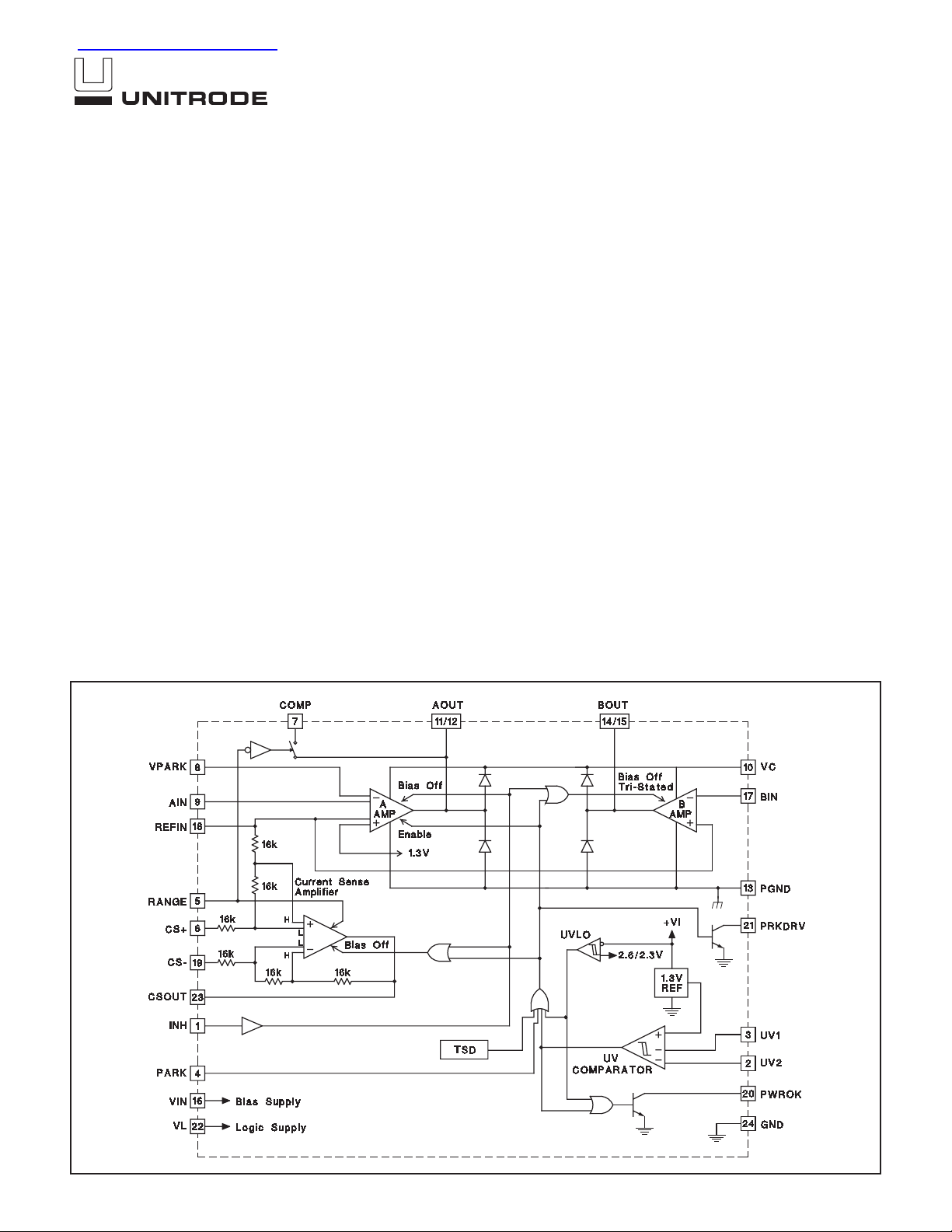
This full bridge power amplifier, rated for continuous output current of
0.55A, is intended for use in demanding servo applications such as head
positioning for high density disk drives. This device includes a precision current sense amplifier that senses load current with a single resistor in series
with the load. The UC3173A is optimized to consume a minimum of supply
current, and is designed to operate in both 5V and 12V systems. The power
output stages have a low saturation voltage and are protected with current
limiting and thermal shutdown. When inhibited the device will draw less
than 1.5mA of total supply current.
Auxiliary functions on this device include a dual input undervoltage comparator, which can monitor two independent supply voltages and activate
the built in head park function when either is below minimum. The park circuitry allows a programmable retract voltage to be applied to the load for
limiting maximum head velocity. A separate low side parking drive pin permits a series impedance to be inserted to control maximum retract current.
The parking drive function can be configured to operate with supply voltages as low as 1.2V.
The closed loop transconductance of the configured power amplifier can be
switched between a high and low range with a logic input. The 4:1 change
in gain can be used to extend the dynamic range of the servo loop. Bandwidth variations that would otherwise result with the gain change can be
controlled with a compensation adjust pin.
BLOCK DIAGRAM
04/99
UDG-94039
UC3173A
ABSOLUTE MAXIMUM RATINGS (Note 1)
Input Supply Voltage, (VIN, VC, VL) . . . . . . . . . . . . . . . . . . 20V
UV Comparator
Maximum Forced Voltage . . . . . . . . . . . . . . . . −0.3V to 10V
Maximum Forced Current. . . . . . . . . . . . . . . . . . . . .±10mA
B Amplifier Inverting Input . . . . . . . . . . . . . . −0.3V to VIN + 1.0
A Amplifier Inverting Inputs,
(Aux. and Normal) . . . . . . . . . . . . . . . . . −0.3V to VC + 1.0V
Open Collector Output Voltages . . . . . . . . . . . . . . . . . . . . . 20V
A and B Output Currents (Continuous)
Source . . . . . . . . . . . . . . . . . . . . . . . . . . . . Internally Limited
Sink . . . . . . . . . . . . . . . . . . . . . . . . . . . . . . . . . . . . . . . . 0.6A
Parking Drive Output Current
Continuous . . . . . . . . . . . . . . . . . . . . . . . . . . . . . . . . 150mA
Pulsed. . . . . . . . . . . . . . . . . . . . . . . . . . . . . . . . . . . . . . . . 1A
Output Diode Current (Pulsed). . . . . . . . . . . . . . . . . . . . . . 0.6A
Power OK Output Current (Continuous). . . . . . . . . . . . . . 30mA
Operating Junction Temperature . . . . . . . . . . −55°C to +150°C
Storage Temperature . . . . . . . . . . . . . . . . . . . −65°C to +150°C
Lead Temperature . . . . . . . . . . . . . . . . . . . . . . . . . . . . . +300°C
Note 1: Unless otherwise indicated, voltages are referenced to
ground and currents are positive into, negative out of, the specified terminals, “Pulsed” is defined as a less than 10% duty cycle
pulse with a maximum duration of 500
µ
s.
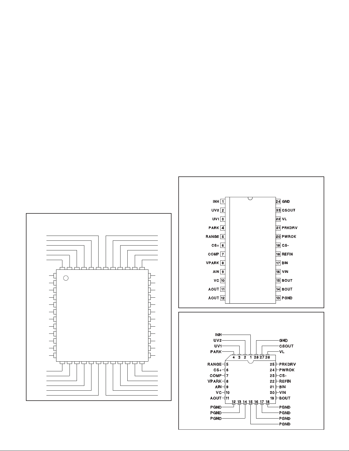
CONNECTION DIAGRAMS
THERMAL DATA
DW Package:
Thermal Resistance Junction to Leads, θjl . . . . . . . . 35°C/W
Thermal Resistance Junction to Ambient, θja . . . . 60-70°C/W
FQ Package:
Thermal Resistance Junction to Leads, θjl. . . . . . . . . 60°C/W
Thermal Resistance Junction to Ambient, θja . . 110-120°C/W
QP Package:
Thermal Resistance Junction to Leads, θjl. . . . . . . . . 15°C/W
Thermal Resistance Junction to Ambient, θja . . . . 30-40°C/W
Note 2: The above numbers forθjl are maximums for the limiting
thermal resistance of the package in a standard mounting configuration. Theθja numbers are meant to be guide lines for the
thermal performance of the device/pc-board system. All of the
above numbers assume no ambient airflow.
Note 3: Consult Packaging Section of Unitrode Integrated Circuits databook for thermal specifications and limitations of packages.
SOIC-24 (Top View)
DW Package
TQFP-48 (Top View)
FQ Package
N/C
N/C
REFIN
CS–
PWROK
PRKDRV
48
46
N/C
VL
CSOUT
GND
N/C
N/C
N/C
N/C
INH
UV2
UV1
PARK
RANGE
CS+
COMP
VP ARK
N/C
47
1
2
3
4
5
6
7
8
9
10
11
12
13
15
14
N/C
N/C
BIN
VIN
N/C
N/C
42
44
43
45
17
18
16
40
393837
41
19
20
23
21
22
N/C
36
35
BOUT
BOUT
34
N/C
33
N/C
32
PGND
31
PGND
30
N/C
29
N/C
28
AOUT
27
26
AOUT
25
N/C
24
N/C
N/C
VC
AIN
N/C
N/CN/C
PLCC-28 (Top View)
QP Package
2
UC3173A
ELECTRICAL CHARACTERISTICS:
Unless otherwise stated, these specifications apply for TA= 0 to +70°C, VIN = 5V,
VC = VIN = VL, REFIN = VIN/2, RANGE, PARK, and INH = 0V, and TA=TJ.
PARAMETER TEST CONDITIONS MIN TYP MAX UNITS
Input Supply
VIN Supply Current 10 13 mA
VC Supply Current I
= 0A 1.2 2.0 mA
OUT
VL Supply Current 0.65 1.0 mA
Total Supply Current Supplies = 5V, I
Supplies = 12V, I
= 0A 12 16 mA
OUT
= 0A 13 18 mA
OUT
VL UVLO Threshold Low to High 2.6 2.8 V
UVLO Threshold Hysteresis 300 mV
Under Voltage (UV) Comparator
Input Bias Current Max at Either UV Input −0.25 −1.0 µA
UV Thresholds Low to High, Other Input = 5V 1.28 1.3 1.32 V
UV Threshold Hysteresis 19 24 29 mV
PWROK Vsat I
PWROK Leakage V
= 5mA, UV Input Low 0.15 0.45 V
OUT
= 20V 5 µA
OUT
Power Amplifiers A and B
Input Offset Voltage A Amplifier, VCM= 2.5V 4 mV
B Amplifier, V
Input Bias Current V
= 2.5V, Inverting Inputs Only −150 −500 nA
CM
Input Bias Current at Ref. Input (REFIN − CS+)/48kΩ,T
CMRR V
= 1V to 10V, Supplies = 12V 70 90 dB
CM
PSRR VIN = 4V to 15V, V
Large Signal Voltage Gain Supplies = 12V, V
V
= 11V, I
OUT
= 2.5V 12 mV
CM
= 25°C 152127µA/V
J
= 1.5V 70 90 dB
CM
OUT
= 1V, I
OUT
= −300mA
= 300mA to
OUT
3.0 15.0 V/mV
Gain Bandwidth Product A Amplifier (Note 4) 2.0 MHz
B Amplifier (Note 4) 1.0 MHz
Slew Rate (Note 4) 1.0 V/µs
High-Side Current Limit Low Range Mode 0.6 0.8 A
High Range Mode 1.1 1.6 A
Output Saturation Voltage High-Side, I
High-Side, I
High-Side, I
Low-Side, I
Low-Side, I
Low-Side, I
Total V
SAT,IOUT
Total V
SAT,IOUT
Total V
SAT,IOUT
VC to VIN Headroom Volts below VIN, delta High-Side, V
= −100mA (Note 5) 0.7 V
OUT
= −300mA (Note 5) 0.8 V
OUT
= −550mA (Note 5) 0.95 V
OUT
= 100mA 0.2 V
OUT
= 300mA 0.25 V
OUT
= 550mA 0.35 V
OUT
= 100mA 0.9 1.2 V
= 300mA 1.05 1.4 V
= 550mA 1.3 1.7 V
= 100mV, I
SAT
0.23 0.4 V
OUT
= −550mA (Note 5)
High-Side Diode, V
Low-Side Diode, V
F
F
ID= 550mA 1.0 V
ID= 550mA, INH Activated, B Amplifer Only 1.0 V
3
UC3173A
ELECTRICAL CHARACTERISTICS:
Unless otherwise stated, these specifications apply for TA= 0 to +70°C, VIN = 5V,
VC = VIN = VL, REFIN = VIN/2, RANGE, PARK, and INH = 0V, and TA=TJ.
PARAMETER TEST CONDITIONS MIN TYP MAX UNITS
Current Sense Amplifier
Input Offset Voltage V
Input Offset Change with Common
Mode Input
Voltage Gain V
Saturation Voltage Low-Side, I
= 2.5V, Low range mode 2.0 mV
CM
= 2.5V, High range mode 4.0 mV
V
CM
= –1V to 13V, Supplies = 12V, Low Range Mode 2000 µV/V
V
CM
= –1V to 13V, Supplies = 12V, High Range Mode 4000 µV/V
V
CM
= +1.0 to −1.0V, VCM= 2.5V, High Range Mode 0.485 0.50 0.515 V/V
DIFF
= +1.0 to −1.0V, VCM= 2.5V, Low Range Mode 1.95 2.0 2.05 V/V
V
DIFF
= 1mA 0.1 0.3 V
OUT
High-Side, I
= −1mA, Referenced to VIN 0.1 0.3 V
OUT
Parking Function
Park Input Threshold Voltage 0.6 1.1 1.7 V
Park Input Threshold Current Internal Pull-Up, VIN = 0.6V 50 75 µA
Park Drive Saturation Voltage I
Park Drive Leakage V
= 50mA 0.15 0.35 V
OUT
= 20V 50 µA
OUT
Regulating Voltage at Park Volts Input 1.275 1.30 1.325 V
Amplifier A Auxiliary Input Bias Current −300 −750 nA
Amplifier A Parking High-Side
Saturation Voltage
= −50mA, VIN = 0V, VC = VL = 5V, PARK Open,
I
OUT
VC to V
OUT
Minimum Parking Supply At VC and VL, VIN = 0V,
A Amplifier Out - V
SAT
PRKDRV > 0.5V, I
PARK
=
0.8 0.95 V
1.4 1.7 V
50mA
Minimum Supply for Parking Drive and
Power OK Operation
At VL, VC = VIN = 0V, V
I
PRKDRV = 50mA, Rl = 30Ω to 2V
OUT
PWROK = 5mA, Rl = 300Ω to 2V 1.2 1.6 V
I
OUT
SAT
< 0.5V,
VL Parking Supply Current PARK Open, VL = 5V, VC = 1.6V, VIN = 0V,
PWROK I
= 5mA, PRKDRV I
OUT
OUT
= 50mA
1.1 1.4 V
1.6 3.0 mA
Auxiliary Functions
Inhibit Input Threshold 0.6 1.1 1.7 V
Inhibit Input Current INH = 1.7V −0.5 −1.0 µA
Range Input Threshold 0.6 1.1 1.7 V
Range Input Current RANGE = 1.7V 50 100 µA
Comp Adjust Pin Saturation Voltage RANGE = 0V, Pin Current = ±500µA,
Referenced to A
OUT
Comp Adjust Leakage Current RANGE = 1.7V, Supplies = 12V,
A
OUT-VCOMP
= ±6V
0.02 0.1 V
5 µA
Total Supply Current when Inhibited VIN, VC, and VL currents 1.0 1.5 mA
Thermal Shutdown Temperature (Note 4) 165 °C
Note 4: Guaranteed by design. Not 100% tested in production.
Note 5: The high-side saturation performance of the UC3173A is referenced to the VIN supply pin.
The VC supply pin can operate about 400mV below the VIN supply input without affecting the performance.
4
 Loading...