

查询UC1875DWP供应商
Phase Shift Resonant Controller
FEATURES
Zero to 100% Duty Cycle Control
•
Programmable Output Turn-On Delay
•
Compatible with Voltage or Current
•
Mode Topologies
Practical Operation at Switching
•
Frequencies to 1MHz
Four 2A Totem Pole Outputs
•
10MHz Error Amplifier
•
Undervoltage Lockout
•
Low Startup Current –150µA
•
Outputs Active Low During UVLO
•
Soft-Start Control
•
• Latched Over-Current Comparator
With Full Cycle Restart
• Trimmed Reference
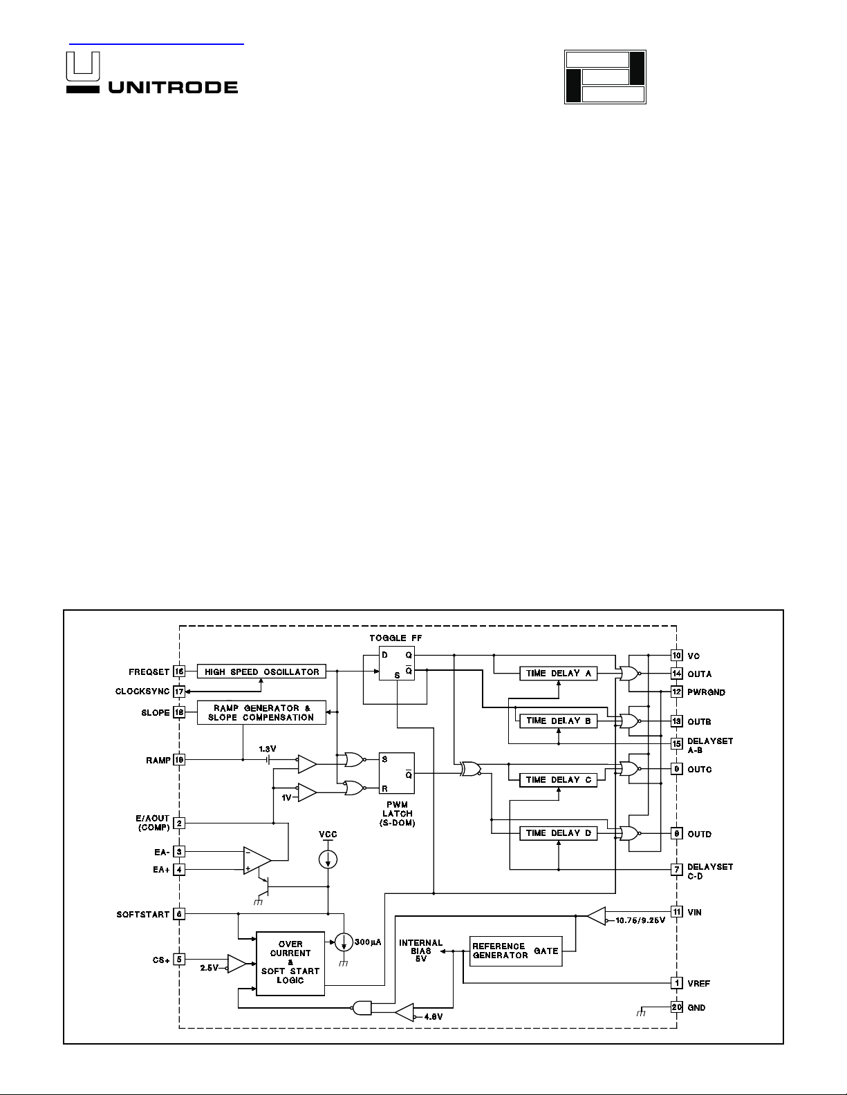
BLOCK DIAGRAM
DESCRIPTION
The UC1875 family of integrated circuits implements control of a bridge
power stage by phase-shifting the switching of one half-bridge with respect
to the other, allowing constant frequency pulse-width modulation in combi
nation with resonant, zero-voltage switching for high efficiency performance
at high frequencies. This family of circuits may be configured to provide
control in either voltage or current mode operation, with a separate
over-current shutdown for fast fault protection.
A programmable time delay is provided to insert a dead-time at the turn-on
of each output stage. This delay, providing time to allow the resonant
switching action, is independently controllable for each output pair (A-B,
C-D).
With the oscillator capable of operation at frequencies in excess of 2MHz,
overall switching frequencies to 1MHz are practical. In addition to the stan
dard free running mode, with the CLOCKSYNC pin, the user may configure
these devices to accept an external clock synchronization signal, or may
lock together up to 5 units with the operational frequency determined by the
fastest device.
Protective features include an undervoltage lockout which maintains all outputs in an active-low state until the supply reaches a 10.75V threshold.
1.5V hysteresis is built in for reliable, boot-strapped chip supply.
Over-current protection is provided, and will latch the outputs in the OFF
state within 70nsec of a fault. The current-fault circuitry implements
full-cycle restart operation.
application
INFO
available
UC1875/6/7/8
UC2875/6/7/8
UC3875/6/7/8
-
-
07/99
UDG-95073
DESCRIPTION (cont.)
Additional features include an error amplifier with band
width in excess of 7MHz, a 5V reference, provisions for
soft-starting, and flexible ramp generation and slope com
pensation circuitry.
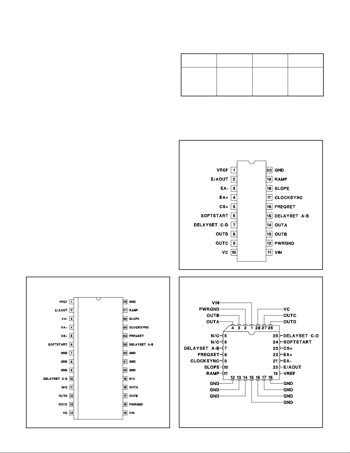
These devices are available in 20-pin DIP, 28-pin
“bat-wing” SOIC and 28 lead power PLCC plastic pack
ages for operation over both 0°C to 70°C and –25°C to
+85°C temperature ranges; and in hermetically sealed
cerdip, and surface mount packages for –55°C to +125°C
operation.
UC1875/6/7/8
UC2875/6/7/8
UC3875/6/7/8
-
-
-
Device UVLO
Turn-On
UC1875 10.75 9.25V Yes
UC1876 15.25V 9.25V Yes
UC1877 10.75V 9.25V No
UC1878 15.25V 9.25V No
UVLO
Turn-Off
Delay
Set
ABSOLUTE MAXIMUM RATINGS
Supply Voltage (VC, VIN) . . . . . . . . . . . . . . . . . . . . . . . . . . 20V
Output Current, Source or Sink
DC . . . . . . . . . . . . . . . . . . . . . . . . . . . . . . . . . . . . . . . . . 0.5A
Pulse (0.5µs). . . . . . . . . . . . . . . . . . . . . . . . . . . . . . . . . . . 3A
Analog I/0s
(Pins 1, 2, 3, 4, 5, 6, 7, 15, 16, 17, 18, 19) . . . . –0.3 to 5.3V
Storage Temperature Range . . . . . . . . . . . . . –65°C to +150°C
Junction Temperature. . . . . . . . . . . . . . . . . . . –55°C to +150°C
Lead Temperature (Soldering, 10 sec.) . . . . . . . . . . . . +300°C
Note: Pin references are to 20 pin packages.All voltages are
with respect to ground.Currents are positive into, negative out of, device terminals. Consult Unitrode
databook for information regarding thermal specifications and limitations of packages.
SOIC-28, (Top View)
DWP Package
CONNECTION DIAGRAMS
Dil-20 (Top View)
J or N Package
PLCC-28 (Top View)
QP Package
2

UC1875/6/7/8
UC2875/6/7/8
UC3875/6/7/8
ELECTRICAL CHARACTERISTICS:
85°C for the UC2875/6/7/8 and 0°C < T
R
SLOPE
= 12kΩ, C
RAMP
= 200pF, C
DELAYSET A-B=CDELAYSET C-D
Unless otherwise stated, –55°C < TA< 125°C for the UC1875/6/7/8, –25°C < TA<
< 70°C for the UC3875/6/7/8, VC = VIN = 12V, R
A
= 0.01µF, I
DELAYSET A-B=IDELAYSET C-D
FREQSET
= 12kΩ,C
FREQSET
= –500µA, TA=TJ.
= 330pF,
PARAMETER TEST CONDITIONS MIN TYP MAX UNITS
Undervoltage Lockout
Start Threshold UC1875/UC1877 10.75 11.75 V
UC1876/UC1878 15.25 V
UVLO Hysteresis UC1875/UC1877 0.5 1.25 2.0 V
UC1876/UC1878 6.0 V
Supply Current
I
Startup VIN = 8V, VC = 20V, R
IN
Startup VIN = 8V, VC = 20V, R
I
C
I
IN
I
C
SLOPE
SLOPE
open, I
open, I
= 0 150 600 µA
DELAY
= 0 10 100 µA
DELAY
30 40 mA
15 30 mA
Voltage Reference
Output Voltage T
= +25°C 4.92 5 5.08 V
J
Line Regulation 11 < VIN < 20V 1 10 mV
Load Regulation I
= –10mA 5 20 mV
VREF
Total Variation Line, Load, Temperature 4.9 5.1 V
Noise Voltage 10Hz to 10kHz 50 µVrms
Long Term Stability T
Short Circuit Current VREF = 0V, T
= 125°C, 1000 hours 2.5 mV
J
= 25°C 60 mA
J
Error Amplifier
Offset Voltage 515mV
Input Bias Current 0.6 3 µA
AVOL 1V < V
CMRR 1.5V < V
< 4V 60 90 dB
E/AOUT
< 5.5V 75 95 dB
CM
PSRR 11V < VIN < 20V 85 100 dB
Output Sink Current V
Output Source Current V
Output Voltage High I
Output Voltage Low I
E/AOUT
E/AOUT
= 1V 1 2.5 mA
E/AOUT
= 4V –1.3 –0.5 mA
E/AOUT
= –0.5mA 4 4.7 5 V
= 1mA 0 0.5 1 V
Unity Gain BW 7 11 MHz
Slew Rate 611 V/µsec
3
UC1875/6/7/8
UC2875/6/7/8
UC3875/6/7/8
ELECTRICAL CHARACTERISTICS:
85°C for the UC2875/6/7/8 and 0°C < T
R
SLOPE
= 12kΩ, C
RAMP
= 200pF, C
DELAYSET A-B=CDELAYSET C-D
Unless otherwise stated, –55°C < TA< 125°C for the UC1875/6/7/8, –25°C < TA<
< 70°C for the UC3875/6/7/8, VC = VIN = 12V, R
A
= 0.01µF, I
DELAYSET A-B=IDELAYSET C-D
FREQSET
= 12kΩ,C
FREQSET
= –500µA, TA=TJ.
= 330pF,
PARAMETER TEST CONDITIONS MIN TYP MAX UNITS
PWM Comparator
Ramp Offset Voltage T
= 25°C (Note 3) 1.3 V
J
Zero Phase Shift Voltage (Note 4) 0.55 0.9 V
PWM Phase Shift (Note1) V
V
Output Skew (Note 1) V
> (Ramp Peak + Ramp Offset) 98 99.5 102 %
E/AOUT
< Zero Phase Shift Voltage 0 0.5 2 %
E/AOUT
< 1V 5 ±20 nsec
E/AOUT
Ramp to Output Delay UC3875/6/7/8 (Note 6) 65 100 nsec
UC1875/6/7/8, UC2875/6/7/8 (Note 6) 65 125 nsec
Oscillator
Initial Accuracy T
= 25°C 0.85 1 1.15 MHz
J
Voltage Stability 11V < VIN < 20V 0.2 2 %
Total Variation Line, Temperature 0.80 1.20 MHz
Sync Pin Threshold T
Clock Out Peak T
Clock Out Low T
= 25°C 3.8 V
J
= 25°C 4.3 V
J
= 25°C 3.3 V
J
Oscillator (cont.)
Clock Out Pulse Width R
Maximum Frequency R
CLOCKSYNC
FREQSET
= 3.9kΩ 30 100 nsec
= 5kΩ 2 MHz
Ramp Generator/Slope Compensation
Ramp Current, Minimum I
Ramp Current, Maximum I
SLOPE
SLOPE
= 10µA, V
= 1mA, V
FREQSET
FREQSET
= VREF –11 –14 µA
= VREF –0.8 –0.95 mA
Ramp Valley 0V
Ramp Peak - Clamping Level R
FREQSET
= 100kΩ 3.8 4.1 V
Current Limit
Input Bias V
+ = 3V 2 5 µA
CS
Threshold Voltage 2.4 2.5 2.6 V
Delay to Output UC3875/6/7/8 85 125 nsec
UC1875/6/7/8, UC2875/6/7/8 85 150 nsec
Soft-Start/Reset Delay
Charge Current V
Discharge Current V
SOFTSTART
SOFTSTART
= 0.5V –20 –9 –3 µA
= 1V 120 230 µA
Restart Threshold 4.3 4.7 V
Discharge Level 300 mV
4
 Loading...