

查询UC1826供应商
Secondary Side Average Current Mode Controller
UC1826
UC2826
UC3826
FEATURES
• Practical Secondary Side Control of
Isolated Power Supplies
• 1MHz Operation
• Tailored Loop Bandwidth Provides
Excellent Noise Immunity
• Voltage Feedforward Provides
Superior T ransient Response
• Accurate Programmable Maximum
Duty Cycle
• Multiple Chips Can be Synchronized
to Fastest Oscillator
• Wide Gain Bandwidth Product
(70MHz, Acl>10) Current Error
Amplifier
• Up to Ten Devices Can Easily Share
a Common Load
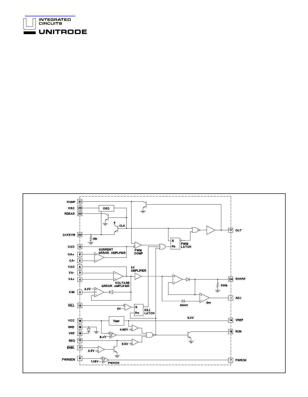
BLOCK DIAGRAM
DESCRIPTION
The UC1826 family of average current mode controllers accurately
accomplishes secondary side average current mode control.The secondary side output voltage is regulated by sensing the output voltage
and differentially sensing the AC switching current.The sensed output
voltage drives a voltage error amplifier.The AC switching current, monitored by a current sense resistor, drives a high bandwidth, low offset
current error amplifier. The output of the voltage error amplifier can be
used to drive the current amplifier which filters the measured inductor
current. Fast transient response is accomplished by utilizing voltage
feedforward in generating the PWM ramp.
The UC1826 features load share, oscillator synchronization, undervoltage lockout, and programmable output control. Multiple chip operation
can be achieved by connecting up to ten UC1826 chips in parallel.The
SHARE bus and CLKSYN bus provide load sharing and synchronization to the fastest oscillator respectively.With its tailored bandwidth, the
UC1826 provides excellent noise immunity and is an ideal controller to
achieve high power, secondary side average current mode control.
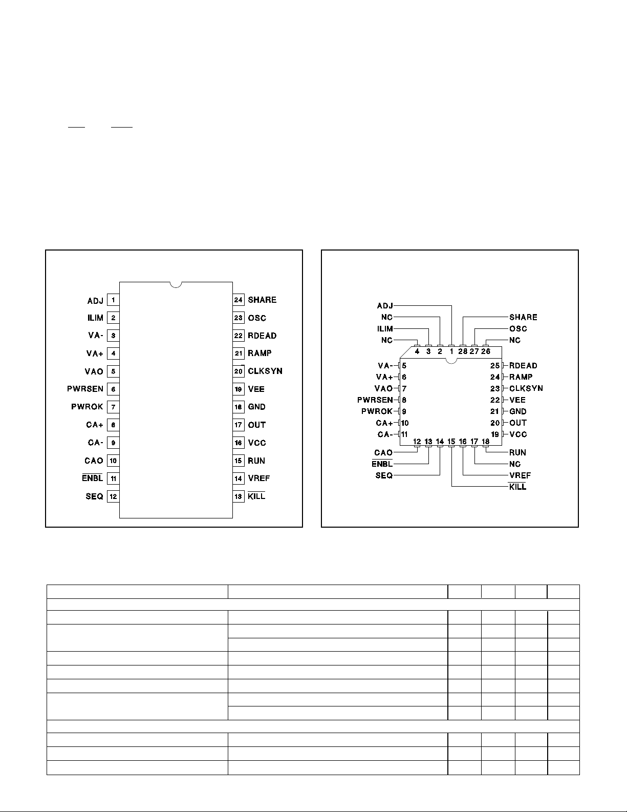
Pin Numbers refer to 24-pin packages.
7/95
UDG-95013
UC1826
UC2826
UC3826
ABSOLUTE MAXIMUM RATINGS
Supply Voltage (VCC) . . . . . . . . . . . . . . . . . . . . . . . . . . . . .20V
Output Current Source or Sink . . . . . . . . . . . . . . . . . . . . . .0.3A
Analog Input Voltages . . . . . . . . . . . . . . . . . . . . . . .−0.3V to 7V
ILIM, KILL, SEQ, ENBL, RUN, PWRSEN, PWROK . . . .−0.3V to 7V
CLKSYN Current Source . . . . . . . . . . . . . . . . . . . . . . . . .20mA
RUN Current Sink . . . . . . . . . . . . . . . . . . . . . . . . . . . . . . .20mA
SEQ Current Sink . . . . . . . . . . . . . . . . . . . . . . . . . . . . . . .20mA
RDEAD Current Sink . . . . . . . . . . . . . . . . . . . . . . . . . . . .20mA
RAMP Current Sink . . . . . . . . . . . . . . . . . . . . . . . . . . . . .20mA
Share Bus Voltage (voltage with respect to GND) . . .0V to 6.2V
ADJ Voltage (voltage with respect to GND) . . . . . .0.9V to 6.3V
VEE (voltage with respect to GND) . . . . . . . . . . . . . . . . . .−1.5V
CONNECTION DIAGRAMS
DIL-24,SOIC-24,TSSOP-24 (Top View)
J or N,DW,PW Packages
Storage Temperature . . . . . . . . . . . . . . . . . . . .−65°C to +150°C
Junction Temperature . . . . . . . . . . . . . . . . . . .−65°C to +150°C
Lead Temperature (Soldering, 10 sec.) . . . . . . . . . . . . .+300°C
All voltages with respect to VEE except where noted;all currents
are positive into, negative out of the specified terminal.
Consult Packaging Section of Databook for thermal limitations
and considerations of packages.
RECOMMENDED OPERATING CONDITIONS
Input Voltage . . . . . . . . . . . . . . . . . . . . . . . . . . . . . . .8V to 20V
Sink/Source Output Current . . . . . . . . . . . . . . . . . . . . . .250mA
Timing Resistor RT . . . . . . . . . . . . . . . . . . . . . . . . . .1k to 200k
Timing Capacitor CT . . . . . . . . . . . . . . . . . . . . . . . .75pF to 2nF
PLCC-28 (Top View)
Q Package
ELECTRICAL CHARACTERISTICSUnless otherwise stated these specifications apply for TA = −55°Cto+125°C for
UC1826;−40°C to +85°C for UC2826;and 0°C to +70°C for UC3826;VCC = 12V, VEE = GND, Output no load, CT = 345pF,
RT = 4kΩ, RDEAD = 1000Ω, CRAMP = 345pF, RRAMP = 35.2kΩ, RCLKSYN = 1k, TA =TJ.
PARAMETER TEST CONDITIONS MIN TYP MAX UNITS
Current Error Amplifier
Ib 0.5 3 µA
Vio TA = +25°C 0.75 3 mV
Over Temperature 5 mV
Avo 60 90 dB
GBW (Note 2) Acl = 10, RIN = 1k, CC = 15pF, f = 200kHz (Note 1) 45 70 MHz
Vol IO = 1mA, Voltage above VEE 0.5 V
Voh IO = 0mA 3.8 V
IO = −1mA 3.5 V
Voltage Error Amplifier
Ib 0.5 3 µA
Vio 5mV
Avo 60 90 dB
2
UC1826
UC2826
UC3826
ELECTRICAL CHARACTERISTICS (cont.)Unless otherwise stated these specifications apply for TA = −55°Cto
+125°C for UC1826;−40°C to +85°C for UC2826;and 0°C to +70°C for UC3826;VCC = 12V, VEE = GND, Output no load, CT =
345pF, RT = 4kΩ, RDEAD = 1000Ω, CRAMP = 345pF, RRAMP = 35.2kΩ, RCLKSYN = 1k, TA = TJ.
PARAMETER TEST CONDITION MIN TYP MAX UNITS
Voltage Error Amplifier (cont.)
GBW (Note 2) f = 200kHz 7 MHz
Vol IO = 175mA, Volts above VEE 0.6 V
V oh ILIM = 3V 2.85 3 3.15 V
Voh-ILIM Tested ILIM = 0.5V, 1.0V, 2.0V −100 100 mV
2X Amplifier and Share Amplifier
V offset (b;y = mx + b) 20 mV
GAIN (m;y = mx + b) Slope with AVOUT = 1V and 2V 1.98 2.02 V
GBW (Note 2) 100 kHZ
RSHARE VCC = 0, VSHARE/ISHARE 200 kΩ
Total Offset Negative supply is VEE, GND Open,VAO = GND −75 0 75 mV
V ol VAO = V oltage Amp Vol, Volts above VEE 0.2 0.45 0.6 V
Voh IO = 0mA, ILIM = 3V, VA O = Voltage Amp V oh 5.7 6 6.3 V
IO = −1mA, ILIM = 3V, VAO = V oltage Amp V oh 5.7 6 6.3 V
Adjust Amplifier
Vio 40 60 80 mV
gm IO = −2µA to 2µA, CADJ = 0.1µF −0.1 −0.3 mS
Vol IOUT = 0 0.9 1 1.1 V
IOUT = 2µA 0.85 1 1.15 V
Voh IOUT = 0, VSHARE = 6.5V 5.7 6 6.3 V
IOUT =−2µA, VSHARE = 6.5V 5.7 6 6.3 V
Oscillator
Frequency 450 500 550 kHz
Max Duty Cycle 72 76 80 %
OSC Ramp Amplitude 2 2.2 2.4 V
Ramp Saturation IO = 10mA, OSC = 0V 0.44 0.8 V
Clock Driver/SYNC (CLKSYN)
Vol 0.02 0.2 V
Voh 3.6 V
RCLKSYN = 200Ω 3.5 V
ISOURCE 25 mA
RCLKSYN VCC = 0, VCLKSYN/ICLKSYN 10 k
VTH 1.5 V
VREF Comparator
T urn-on Threshold 4.65 V
Hysteresis 0.4 V
VCC Comparator
T urn-on Threshold 7.9 8.4 8.9 V
Hysteresis 0.4 V
PWR Sense Comparator
V oltage Threshold 1.25 V
Vol IO = 1mA 0.3 0.4 V
Voh IO =−100µA4V
KILL Comparator
V oltage Threshold 3V
3
UC1826
UC2826
UC3826
ELECTRICAL CHARACTERISTICS (cont.)Unless otherwise stated these specifications apply for TA = −55°Cto
+125°C for UC1826;−40°C to +85°C for UC2826;and 0°C to +70°C for UC3826;VCC = 12V, VEE = GND, Output no load, CT =
345pF, RT = 4kΩ, RDEAD = 1000Ω, CRAMP = 345pF, RRAMP = 35.2kΩ, RCLKSYN = 1k, TA = TJ.
PARAMETER TEST CONDITION MIN TYP MAX UNITS
Sequence Comparator
V oltage Threshold 2.5 V
SEQ SAT IO = 10mA 0.25 V
Enable Comparator
V oltage Threshold 2.5 V
RUN SAT IO = 10mA 0.2 V
Reference
VREF TA = 25°C 4.95 5 5.05 V
VCC = 15V 4.9 5.1 V
Line Regulation 10 < VCC < 20 3 15 mV
Load Regulation 0 < IO < 10mA 3 15 mV
Short Circuit I VREF = 0V 30 60 90 mA
Output Stage
Rise Time CL = 100pF 10 20 ns
Fall Time CL = 100pF 10 20 ns
Voh VCC > 11V, IO =−10mA 8.0 8.4 8.8 V
IO = −200mA 7.8 V
Vol IO = 200mA 3.0 V
IO = 10mA 0.5 V
Virtual Ground
V
GND − VEE VEE is externally supplied, GND is floating 0.2 0.75 V
and used as Signal GND.
Icc
Icc (run) 21 30 mA
Note 1: Guaranteed by design.Not 100% tested in production.
Note 2: Unless otherwise specified all voltages are with respect to GND.Currents are positive into, negative out of the
specified terminal.
PIN DESCRIPTIONS
ADJ: The output of the transconductance (gm = −0.1mS)
amplifier adjusts the control voltage to maintain equal current sharing.The chip sensing the highest output current
will have its output clamped to 1V. A resistor divider
between VREF and ADJ drives the control voltage (VA+)
for the voltage amplifier. Each slave unit’s ADJ voltage
increases (to a maximum of 6V) its control voltage (VA+)
until its load current is equal to the master.The 60mV
input offset on the gm amplifier guarantees that the unit
sensing the highest load current is chosen as the master.
The 60mV offset is guaranteed by design to be greater
than the inherent offset of the gm amplifier and the buffer
amplifier. While the 60mV offset represents an error in
current sharing, the gain of the current and 2X amplifiers
reduces it to only 30mV. The total current sense gain is
the current amplifier gain.This pin needs a 0.1µF capaci-
tor to compensate the amplifier.
CA-, CA+: The inverting and non-inverting inputs to the
current error amplifier. This amplifier needs a capacitor
between CA- and CAO to set its dominant pole.
CAO: The output of the current error amplifier which is
internally clamped to 4V.It is internally connected to the
inverting input of the PWM comparator.
CLKSYN: The clock and synchronization pin for the
oscillator. This is a bidirectional pin that can be used to
synchronize several chips to the fastest oscillator. Its
input synchronization threshold is 1.4V. The CLKSYN
voltage is 3.6V when the oscillator capacitor CT is being
discharged, otherwise it is 0V.
4

PIN DESCRIPTIONS (cont.)
ENBL: The active low input with a 2.5V threshold
enables the output to switch. SEQ and RUN are driven
low when ENBL is above its 2.5V threshold.
GND: The signal ground used for the voltage sense
amplifier, current error amplifier, current error amplifier,
voltage reference, 2X amplifier, and share amplifier.The
output sink transistor is wired directly to this pin.
KILL: The active low input with a 3.0V threshold stops
the output from switching.Once this function is activated
RUN must be cycled low by driving KILL above 3.0V and
either resetting the power to the chip (VCC) or resetting
the ENBL signal.
ILIM: A voltage on this pin programs the voltage error
amplifier’s Voh clamp. The voltage error amplifier output
represents the average output current. The Voh clamp consequently limits the output current.If ILIM is tied to VREF, it
defaults to 3.0V. A voltage less than 3.0V connected to
ILIM clamps the voltage error amplifier at this voltage and
consequently limits the maximum output current.
OSC:The oscillator ramp (not to be confused with PWM
ramp) pin has a capacitor CT to ground and two resistors
in series RT and RDEAD to VREF. The total resistance of
RT and RDEAD divided by VREF − VOSC sets exponential
charge current.The oscillator charges from 1.2V to 3.4V
until the output transitions low. At this time an open collector transistor is turned on and discharges the CT
capacitor through RDEAD.
The charge time is approximately TCHARGE = 2(RT +
RDEAD) ·CT when the RDEAD resistor is used.
The dead time is approximately TDISCHARGE = 2 · RDEAD ·
CT.
(1) Frequency ≈
TCHARGE + TDISCHARGE
(2) Maximum Duty Cycle ≈
The CT capacitance should be increased by approximately 40pF to account for parasitic capacitance.
OUT: The output of the PWM driver. It has an upper
clamp of 8.5V. The peak current sink and source are
250mA. All UVLO, SEQ, ENBL, and KILL logic either
enable or disable the output driver.
PWRSEN: This pin is the input to the PWROK comparator.
PWROK: The output pin from the PWROK comparator.It
has a 300µA current source output when driven high.
RAMP: An open collector that can sink 20mA to dis-
charge the oscillator capacitor. An RC is tied between
1
TCHARGE
TCHARGE + TDISCHARGE
UC1826
UC2826
UC3826
VCC and GND to accomplish feedforward. The PWM
output drives this pin.When the output is high, the transistor is off enabling the charging of the RAMP capacitor.
When the output transitions low, the transistor is turned
on discharging the RAMP capacitor. The voltage at
RAMP rises from 0.2V to near 4V at maximum duty
cycle. Although this is an exponential ramp at high VCC
voltage the ramp appears linear.
RDEAD: The pin that programs the maximum duty cycle
by connecting a resistor between it and OSC. The maximum duty cycle is decreased by increasing this resistor
value which increases the discharge time. The dead
time, the time when the output is low, is 2 ·RDEAD·CT.
The CT capacitance should be increased by approximately 40pF to account for parasitic capacitance.
RUN: This is an open collector logic output that signifies
when the chip is operational.RUN is pulled high to VREF
through an external resistor when VCC is greater than
8.4V, VREF is greater than 4.65V, SEQ is greater than
2.5V, and KILL lower than 3.0V. RUN connected to the
VA+ pin and to a capacitor to ground adds an RC rise
time on the VA+ pin initiating a soft start.
SEQ: The sequence pin allows the sequencing of startup
for multiple units.A resistor between VREF and SEQ and
a capacitor between SEQ and GND create a unique RC
rise time for each unit which sequences the output startup.
SHARE:The nearly DC voltage representing the average
output current. This pin is wired directly to all SHARE
pins and is the load share bus.
VA-, VA+: The inverting and non-inverting inputs to the
voltage error amplifier.
VAO: The output of the voltage error amplifier.Its Voh is
clamped with the ILIM pin.
VCC: The input voltage to the chip. The chip is operational between 8.4V and 20V.
VEE: The negative supply voltage to the chip which powers the lower voltage rail for all amplifiers. The chip is
operational if VEE is connected to GND or if GND is
floating.When voltage is applied externally to VEE, GND
becomes a virtual ground because of an internal diode
between VEE and GND. The GND current flows through
the forward biased diode and out VEE. GND is always
the signal ground from which the voltage reference and
all amplifier inputs are referenced.
VREF: The reference voltage equal to 5.0V.
5

UC1826
UC2826
UC3826
Figure 1.Oscillator Block with External Connections
CIRCUIT DESCRIPTION:
PWM Oscillator: The chip has two pins that set RC time
constants.The resistor and capacitor tied to RAMP create the ramp used as the input to the PWM comparator.
When the output pin OUT is high, RAMP charges until it
passes the PWM comparator threshold. The output is
then driven low and RAMP is discharged. The resistors
and capacitor on the OSC pin are used to set the PWM
operating frequency and its maximum duty cycle.
The oscillator block diagram with external wiring is
shown in Figure 1. OSC has a capacitor (CT) to ground
and two resistors in series (RT and RDEAD) to VREF.The
total resistance of RT and RDEAD divided by VREF −
VOSC sets the exponential charge current.The oscillator
charges from 1.2V to a 3.4V threshold with an RC time
3.0-
OSC
1.0
CLKSYN
OUT
CAO
RAMP
Figure 2.Oscillator and PWM Output Waveform
UDG-95014-1
delay of 2 ·CT·(RDEAD + RT). After exceeding this
threshold, the RS flip-flop is set driving CLKSYN high
and RDEAD low which discharges CT. At this time and
open collector transistor is turned on and discharges CT
capacitor through RDEAD with a RC time delay of 2
CT· RDEAD. The oscillator and ramp waveforms are
shown in Figure 2. Equations to attain frequency and
maximum duty cycle are listed under the OSC pin
description.
As shown in Figure 3, several oscillators are synchronized to the highest free running frequency by connecting 100pF capacitors in series with each CLKSYN pin
and connecting the other side of the capacitors together
forming the CLKSYN bus. The CLKSYN bus is then
pulled down to ground with a resistance of approximately
10k. Referring to Figure 1, the synchronization threshold
is 1.4V. The oscillator blanks any synchronization pulse
that occurs when OSC is below 2.5V. This allows units,
once they discharge below 2.5V, to continue through the
current discharge and subsequent charge cycles
whether or not other units on the CLKSYN bus are still
synchronizing.This requires the frequency of all free running oscillators to be within 40% of each other to guarantee synchronization.
Grounds,Voltage Sensing and Current Sensing: The
voltage is sensed directly at the load. Proper load sharing requires the same sensed voltage for each power
supply connected in parallel. Referring to Figure 4, the
·
6

CIRCUIT BLOCK DESCRIPTION (cont.)
Figure 3.Oscillator Synchronization
Connection Diagram
UDG-95015
UC1826
UC2826
UC3826
Figure 4 shows one recommended voltage and current
sensing scheme when VEE is connected to GND. The
signal ground is the negative sense point for the output
voltage and the positive sense point for the output current. VEE is the negative supply for the current sense
amplifier.When it is separated from GND, it extends the
current sense amplifier’s common mode input voltage
range to include VEE which is approximately −0.7V
below ground.The resistor RADJ is used for load sharing.
The unit which is the master will force VADJ to 1.0V.
Therefore, the regulated voltage being sensed is actually
RADJ
VSP − VSM = (VREF − VADJ)
VSM = 0V, VADJ = 1V (master), VREF = 5V
RADJ
VSP = 4
The voltage at ADJ on the slave chips will increase forcing their load currents to increase to match the master.
The AC frequency response of the voltage error amplifier
is shown in Figure 5.
()
·
R1 + RADJ
· ()
R1 + RADJ
+ 1V
+VADJ
positive sense voltage (VSP) connects to the voltage
error amplifier inverting terminal (VA-), the return lead for
the on-chip reference is used as the negative sense
(VSM). The current is sensed across the shunt resistor,
RS.The voltage across the shunt resistor is level shifted
up so that the maximum voltage across Rs corresponds
to the voltage error amplifier Voh.
UDG-95016
Figure 4.Voltage and Current Sense VEE Tied to GND
∅ ≈m
Figure 5.AC Frequency Response of the Voltage
Error Amplifier
Startup and Shutdown: Isolated power up can be
accomplished using the UCC1889. Application Note
U-149 is available for additional information.
The UC1826 offers several features that enhance startup
and shutdown. Soft start is accomplished by connecting
RUN to VA+ and a capacitor to ground.The resulting RC
rise time on the VA+ pin initiates a soft star t. It can also
be accomplished by connecting RUN to ILIM. When RUN
is low it will command zero load current, guaranteeing a
soft start. The undervoltage lockout (UVLO) is a logical
AND of ENBL < 2.5V, SEQ > 2.5V, VCC > 8.4V and
7

CIRCUIT BLOCK DESCRIPTION (cont.)
VREF > 4.65V.The block diagram shows that the thresholds are set by comparators.By placing an RC divider on
the SEQ pin, the enabling of multiple chips can be
sequenced with different RC time constants. Similarly,
different RC time constants on the ENBL pins can
sequence shutdown. The UVLO keeps the output from
switching; however the internal reference starts up with
VCC less than 8.4V. The KILL input shuts down the
switching of the chip. This can be used in conjunction
with an overvoltage comparator for overvoltage protection.In order to restar t the chip after KILL has been initiated, the chip must be powered down and then back up.
A pulse on the ENBL pin also accomplishes this without
actually removing voltage to the VCC pin.
Load Sharing: Load sharing is accomplished similar ly to
the UC1907 except it has the added constraint of using
the sensed current for average current mode control.The
sensed current for the UC1826 has an AC component
that is amplified and then averaged. The voltage error
amplifier represents this average current. The voltage
error amplifier output is the current command signal and
its voltage represents the average output load current.
The ILIM pin programs the upper clamp voltage of this
amplifier and consequently the maximum load current.A
gain of 2 amplifier connected between the voltage error
amplifier output and the share amplifier input increases
the current share resolution and noise margin.The average current is used as an input to a source only load
share buffer amplifier.The output of this amplifier is the
current share bus.The IC with the highest sensed current will have the highest voltage on the current share
bus and consequently act as the master.The 60mV input
offset guarantees that the unit sensing the highest load
current is chosen as the master.
UC1826
UC2826
UC3826
Current Control Loop: The current error amplifier (CEA)
needs its loop compensated externally.The zero crossing
can be calculated with Equation 3.
(3) Frequency (0dB) =
2π RINV· CCOMP
RINV is the input resistance at the inverting ter minal CACCOMP is the capacitance between CA- and CAO.
Although it is only unity gain stable for a BW of 7MHz,
the amplifier is typically configured with a differential gain
of at least 10, allowing the amplifier to operate with sufficient phase margin at a GBW of 70MHz. A closed loop
gain of 10 attenuates the output by 20.8dB
1
20.8 = 20log
·
11
to the inverting terminal assuring stability. The amplifier’s
gain fed back into the inverting terminal is less than unity
at 7MHz, where the phase margin begins to roll off.See
Figure 6 for a typical Bode plot.
−
1
β
∅m
The adjust amplifier is used by the remaining (slave) ICs
to adjust their respective references high in order to balance each IC’s load current. The master’s ADJ pin will be
at its 1.0V clamp and connected back to the non-inverting voltage error amplifier input through a high value
resistor. This requires the user to initially calculate the
control voltage with the ADJ pin at 1.0V.
VREF can be adjusted 150mV to 300mV which compensates for 5% unit to unit reference mismatch and external
resistor mismatch. RADJ will typically be 10 to 30 times
larger than R1.This also attenuates the overall variation of
the ADJ clamp of 1V ±100mV by a factor of 10 to 30, contributing only a 3mV to 10mV additional delta to VREF.
Refer to the UC3907 Application Note U-130 for further
information on parallel power supply load sharing.
Figure 6.Current Error Amplifier Bode Plot
The current error amplifier bandwidth is rolled off and
controlled by the voltage error amplifier output.The maximum load current is limited to approximately the maximum voltage across the shunt resistor (maximum of
200mV) divided by RS:
(4) IMAXload =
VRs
RS
ILIM sets the maximum current limit by setting the Voh
clamp on the voltage error amplifier. If ILIM is not set to
limit the Voh to be equal to the maximum voltage across
RS, VAO must be attenuated to match the maximum volt-
8

CIRCUIT BLOCK DESCRIPTION (cont.)
age VRS across the shunt resistor. By attenuating the
maximum voltage at VAO to be equal to VRS, the current
control loop keeps the load from exceeding its current
limit. If the ILIM pin is connected to VREF, the Voh is set
at 3.0V. The maximum current limit clamp can be
reduced by reducing the voltage on ILIM to less than
3.0V as described in the ILIM pin description.
UC1826
UC2826
UC3826
Design Example: Figure 7 is an open loop test that lets
the user test the circuit blocks discussed without having
to build an entire control loop. The pulse width can be
varied by either the VADJ or the VISENSE inputs. Figure 8
shows an isolated power supply using the UC1826 secondary side average current mode controller.
Figure 7.Open Loop Circuit
9
UDG-95017-1

UC1826
UC2826
UC3826
UNITRODE INTEGRATED CIRCUITS
7 CONTINENTAL BLVD. • MERRIMACK, NH 03054
TEL.603-424-2410 • FAX 603-424-3460
Figure 8.UC1826 Application Diagram
10

IMPORTANT NOTICE
T exas Instruments and its subsidiaries (TI) reserve the right to make changes to their products or to discontinue
any product or service without notice, and advise customers to obtain the latest version of relevant information
to verify, before placing orders, that information being relied on is current and complete. All products are sold
subject to the terms and conditions of sale supplied at the time of order acknowledgement, including those
pertaining to warranty, patent infringement, and limitation of liability.
TI warrants performance of its semiconductor products to the specifications applicable at the time of sale in
accordance with TI’s standard warranty. Testing and other quality control techniques are utilized to the extent
TI deems necessary to support this warranty . Specific testing of all parameters of each device is not necessarily
performed, except those mandated by government requirements.
CERTAIN APPLICATIONS USING SEMICONDUCTOR PRODUCTS MAY INVOLVE POTENTIAL RISKS OF
DEATH, PERSONAL INJURY, OR SEVERE PROPERTY OR ENVIRONMENTAL DAMAGE (“CRITICAL
APPLICATIONS”). TI SEMICONDUCTOR PRODUCTS ARE NOT DESIGNED, AUTHORIZED, OR
WARRANTED TO BE SUITABLE FOR USE IN LIFE-SUPPORT DEVICES OR SYSTEMS OR OTHER
CRITICAL APPLICA TIONS. INCLUSION OF TI PRODUCTS IN SUCH APPLICATIONS IS UNDERST OOD TO
BE FULLY AT THE CUSTOMER’S RISK.
In order to minimize risks associated with the customer’s applications, adequate design and operating
safeguards must be provided by the customer to minimize inherent or procedural hazards.
TI assumes no liability for applications assistance or customer product design. TI does not warrant or represent
that any license, either express or implied, is granted under any patent right, copyright, mask work right, or other
intellectual property right of TI covering or relating to any combination, machine, or process in which such
semiconductor products or services might be or are used. TI’s publication of information regarding any third
party’s products or services does not constitute TI’s approval, warranty or endorsement thereof.
Copyright 1999, Texas Instruments Incorporated
 Loading...