

Page 1
DESCRIPTION
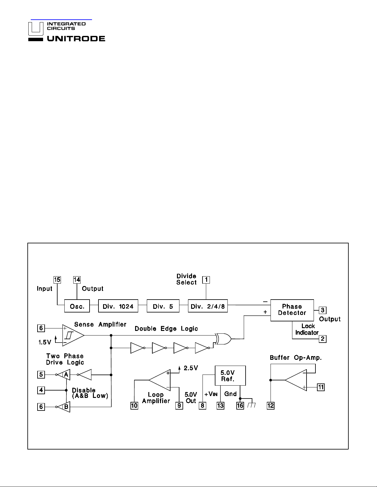
The UC1634 serie s of devices is optimized to provide precision
phase locked frequency control for two phase DC brushless motors. These devices include most of the features of the general
purpose UC1633 Phase Locked Control family and also provide
the out-of-phase commutation signals required for driving two
phase brushless motors. Only an external power booster stage
is required for a complete drive and control system.
The two commutation outputs are open collector devices that can
sink in excess of 16mA. A disable input allows the user to simultaneously force both of these outputs to an active low state.
Double edge logic, followin g the sense amplifier, doubles the reference frequency at the phase detector by responding to both
edges of the input signal at Pin 7.
查询UC1634供应商
Phase Locked Frequency Controller
FEATURES
• Precision Phase Locked Frequency Control
System
• Communication Logic for 2-Phase Motors
• Disable Input for Motor Inhibit
• Crystal Oscillator
• Programmable Reference Frequency Dividers
• Phase Detector with Absolute Frequency
Steering
• Digital Lock Indicator
• Two High Current Op-Amps
UC1634
UC2634
UC3634
• 5V Reference Output
BLOCK DIAGRA M
6/93
Page 2
ABSOLUTE MAXI MUM RATING S (Note 1, 2)
Unless other wise stat ed, these specif icat ions ap ply fo r TA = 0°C to +70°C for the
UC3634, -25°C to + 85°C for the UC2634 and -55°C t o +125°C for the UC1634 ,
+VIN
=
12V. TA=TJ.
Input Supply Volt age ( +VI N). . . . . . . . . . . . . . . . . . . . . . . . +20V
Reference Output Current . . . . . . . . . . . . . . . . . . . . . . . -30mA
Op-Amp Output Currents . . . . . . . . . . . . . . . . . . . . . . . . ±±30mA
Op-Amp Input Volt ages . . . . . . . . . . . . . . . . . . . . . -.3V to +20V
Phase Detec to r Output Cur ren t . . . . . . . . . . . . . . . . . . . ±±10mA
Lock Indicato r Output Cur ren t . . . . . . . . . . . . . . . . . . . . +15mA
Lock Indicato r Output Volt age . . . . . . . . . . . . . . . . . . . . . . +20V
Divide Select Input Voltage . . . . . . . . . . . . . . . . . . -.3V to +10V
Disable Input Voltage. . . . . . . . . . . . . . . . . . . . . . . -.3V to +10V
Oscillator In put Voltage . . . . . . . . . . . . . . . . . . . . . . -.3V to +5V
Sense Amplifier Input Volta ge . . . . . . . . . . . . . . . . -.3V to +20V
Driver Outp ut Curr ent s. . . . . . . . . . . . . . . . . . . . . . . . . . +30mA
Driver Output Voltag es. . . . . . . . . . . . . . . . . . . . . . . . . . . . +20V
Power Dissipation at T
Power Dissipation at T
Operating Junct ion Te mp era tu re . . . . . . . . . . . -55°C to +150°C
Storage Temperature. . . . . . . . . . . . . . . . . . . . -65°C to +150°C
Lead Tempera tu re (Solderin g, 10 Seconds) . . . . . . . . . . 300°C
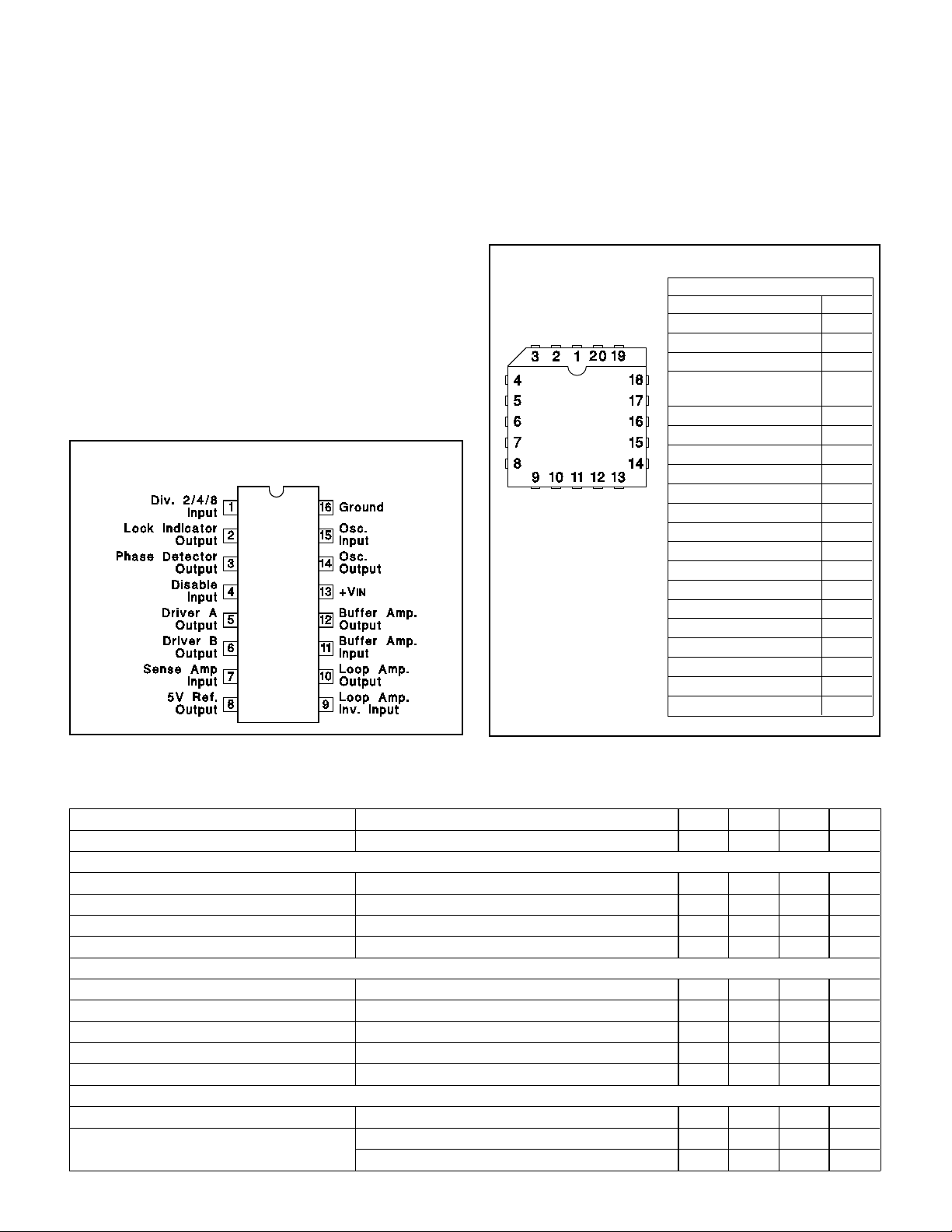
DIL-16, SOIC- 16 (T O P VIEW)
J or N Package, DW Package
A = 25°C(Note 2) . . . . . . . . . . . 1000mW
C = 25°C (Note 2). . . . . . . . . . . 2000mW
UC1634
UC2634
UC3634
Note 1: V olta ges ar e refe ren ced t o ground , (P in 16, DIL Pack age). Curre nts are posit ive into , negat ive out of , the specifi ed
terminals.
Note 2: Consult Packag in g Sect ion of Dat aboo k for ther ma l
limitations and con sider atio ns of pack age.
CONNECTION DIAGRAMS
PLCC-20 (TOP VIEW)
Q Package
PACKAGE PIN FUNCTION
FUNCTION PIN
N/C 1
DIV 2/4/8 2
Lock Indicator Outp ut 3
Phase Detector
Output
Disable Input 5
N/C 6
Driver A Output 7
Driver B Output 8
Sense Amp Output 9
5V Ref Output 10
Loop Amp Inv Input 11
Loop Am p Ou tp ut 12
Buffer Amp Input 13
Buffer Amp Out put 14
+V
IN 15
N/C 16
OSC Output 17
OSC Input 18
Ground 19
DIV 4/5 Input 20
4
ELECTRICAL CHARACTERISTICS:
PARAMETERS TEST CONDITIONS MIN TYP MAX UNITS
Supply Current +VIN = 15V 20 29 mA
Reference
Output Volt age ( VREF
Load Regulation IOUT = 0mA to 7mA 5.0 20 mV
Line Regulatio n +VIN = 8V to 15V 2.0 20 mV
Short Circuit Current VOUT = 0V 12 30 mA
Oscillator
DC Voltage Gain Oscillator In to Oscillator Out 12 16 20 dB
Input DC Level (VIB) Oscillator In Pin Open, TJ = 25°C 1.15 1.3 1.45 V
Input Impedance (Note 3) VIN = VIB
Output DC Level Oscillator In Pin Open, TJ = 25°C 1.2 1.4 1.6 V
Maximum Operating Frequency 10 MHz
Dividers
Maximum Input Frequency Input = 1VPP at Oscillator In 10 MHz
Div. 4/5 Input Current Input = 5V (Div. by 4) 150 5 00 µA
(Q Package Only, Note 4) Input = 0V (Div. by 5) -5.0 0.0 5.0 µA
)
±
0.5V, T
J = 25°C 1.3 1.6 1.9 kΩ
2
4.75 5.0 5.25 V
Page 3

Unless other wise stat ed, these specif icat ions ap ply fo r TA = 0°C to +70°C for the
UC3634, -25°C to + 85°C for the UC2634 and -55°C t o +125°C for the UC1634 ,
+VIN
=
12V. TA=TJ
ELECTRICAL CHARACTERISTICS:
PARAMETERS TEST CONDITIONS MIN TYP MAX UNITS
Dividers (co nt.)
Div. 4/5 Input Threshold
(Q Package Only, Note 4)
Div. 2/4/8 Input Current Input = 5V (Div. by 8) 150 5 00 µA
Input = 0V (Div. by 2) -500 -150 µA
Div. 2/4/8 Open Cur ren t Voltage Input Current = 0 µ A (Div. by 4) 1.5 2.5 3.5 V
Div. by 2 Threshold 0.20 0.8 V
Div. by 4 Threshold 1.5 3.5 V
Div. by 8 Threshold Volts Below V
Sense Amplifier
Threshold Volta ge Percent of V REF 27 30 33 %
Threshold Hyst eresis 10 mV
Input Bias Cur rent Input = 1.5 V -1.0 -0.2 µA
Two Phase Dri ve Ou tpu ts, A and B
Saturation Volta ge IOUT = 16mA 0.3 0.6 V
Leakage Current VOUT = 15V 0.1 5.0 µA
Disable Inpu t
Input Curren t Input = 5V (Disabled, A and B Output s Act ive Low) 150 5 00 µA
Input = 0V (Enabled) -5.0 0.0 5.0 µA
Threshold Voltage 0.5 1. 6 2.2 V
Phase Detector
High Output Level Positive Phase / Freq. Error, Volt s Below VREF 0.2 0.5 V
Low Output Level Negative Pha se / Freq . Error 0.2 0.5 V
Mid Output Level Zero Phase / Freq. Error, Percent of VREF 47 50 53 %
High Level Maximum Sour ce Curre nt VOUT = 4.3 V 2.0 8.0 mA
Low Level Maximum Sink Curre nt VOUT = 0.7V 2.0 5.0 mA
Mid Level Output Imp edan ce (Note 3) IOUT = -200 t o +200 µA, TJ = 25°C 4.5 6.0 7.5 kΩ
Lock In di cat or O ut p ut
Saturation Volta ge Freq. Error, IOUT = 5mA 0.3 0.4 5 V
Leakage Current Zero Freq. Error, VOUT = 15V 0.1 1.0 µA
Loop Amplifier
N INV. Refer ence Voltage Percent of VREF 47 50 53 %
Input Bias Cur rent Input = 2.5 V -0.8 -0.2 µA
AVOL 60 75 dB
PSRR +VIN = 8V to 15V 70 100 dB
Short Circuit Current Source, VOUT = 0V 16 35 mA
Sink , VOUT = 5V 16 30 mA
Buffer Op-Am p
Input Offs et Vo lta ge VCM = 2.5V 8 mV
Input Bias Cur rent VCM = 2.5V -0.8 -0.2 µA
PSRR +VIN = 8 to 15V 70 100 dB
CMRR VCM = 0 to 10V 70 100 dB
Short Circuit Current Source, VOUT = 0V 16 35 mA
Sink , VOUT = 5V 16 30 mA
REF 0.20 0.8 V
Note 3: These impedance levels w i ll vary with TJ at about 1700ppm/°C.
Note 4: This part is also available in a 20 pin plastic leadless chip carrier, Q designa to r , wher e a divide by 4/5 select pin is available.
Consult factory for details.
3
0.5 1. 6 2.2 V
UC1634
UC2634
UC3634
Page 4

UC1634
UC2634
UC3634
APPLICATION AND OPE RATI ON INFO RMATI ON
(For additional information see UC1633 data sheet)
Design Example :
Precision phased locked frequency control of a 2-phase motor at 3600 RPM. Using the commutation logic on the
UC3634, a simple discrete drive scheme is possible.
UNITRODE INTEGRATED CIRCUITS
7 CONTINENTAL BL VD. • • MERRIMACK, NH 03054
TEL. (603) 424-2410 • FAX (603) 424-3460
4
Page 5

IMPORTANT NOTICE
T exas Instruments and its subsidiaries (TI) reserve the right to make changes to their products or to discontinue
any product or service without notice, and advise customers to obtain the latest version of relevant information
to verify, before placing orders, that information being relied on is current and complete. All products are sold
subject to the terms and conditions of sale supplied at the time of order acknowledgement, including those
pertaining to warranty, patent infringement, and limitation of liability.
TI warrants performance of its semiconductor products to the specifications applicable at the time of sale in
accordance with TI’s standard warranty. Testing and other quality control techniques are utilized to the extent
TI deems necessary to support this warranty . Specific testing of all parameters of each device is not necessarily
performed, except those mandated by government requirements.
CERTAIN APPLICA TIONS USING SEMICONDUCT OR PRODUCTS MAY INVOLVE POTENTIAL RISKS OF
DEATH, PERSONAL INJURY, OR SEVERE PROPERTY OR ENVIRONMENTAL DAMAGE (“CRITICAL
APPLICATIONS”). TI SEMICONDUCTOR PRODUCTS ARE NOT DESIGNED, AUTHORIZED, OR
WARRANTED TO BE SUITABLE FOR USE IN LIFE-SUPPORT DEVICES OR SYSTEMS OR OTHER
CRITICAL APPLICA TIONS. INCLUSION OF TI PRODUCTS IN SUCH APPLICATIONS IS UNDERST OOD TO
BE FULLY AT THE CUSTOMER’S RISK.
In order to minimize risks associated with the customer’s applications, adequate design and operating
safeguards must be provided by the customer to minimize inherent or procedural hazards.
TI assumes no liability for applications assistance or customer product design. TI does not warrant or represent
that any license, either express or implied, is granted under any patent right, copyright, mask work right, or other
intellectual property right of TI covering or relating to any combination, machine, or process in which such
semiconductor products or services might be or are used. TI’s publication of information regarding any third
party’s products or services does not constitute TI’s approval, warranty or endorsement thereof.
Copyright 1999, Texas Instruments Incorporated
 Loading...