

Page 1
查询5962-8670405PA供应商
Current Mode PWM Controller
FEATURES DESCRIPTION
Optimized for Off-line and DC to DC
•
Converters
Low Start Up Current (<0.5mA)
•
Trimmed Oscillator Discharge Current
•
Automatic Feed Forward Compensation
•
Pulse-by-Pulse Current Limiting
•
Enhanced Load Response Characteristics
•
Under-Voltage Lockout With Hysteresis
•
Double Pulse Suppression
•
High Current Totem Pole Output
•
Internally Trimmed Bandgap Reference
•
• 500kHz Operation
• Low R
O Error Amp
The UC1842A/3A/4A/5A family of control ICs is a pin for pin compati
ble improved version of the UC3842/3/4/5 family. Providing the nec
essary features to control current mode switched mode power
supplies, this family has the following improved features. Start up cur
rent is guaranteed to be less than 0.5mA. Oscillator discharge is
trimmed to 8.3mA. During under voltage lockout, the output stage
can sink at least 10mA at less than 1.2V for V
The difference between members of this family are shown in the table
below.
Part # UVLO On UVLO Off
UC1842A 16.0V 10.0V <100%
UC1843A 8.5V 7.9V <100%
UC1844A 16.0V 10.0V <50%
UC1845A 8.5V 7.9V <50%
application
INFO
available
UC1842A/3A/4A/5A
UC2842A/3A/4A/5A
UC3842A/3A/4A/5A
-
-
-
CC over 5V.
Maximum Duty
Cycle
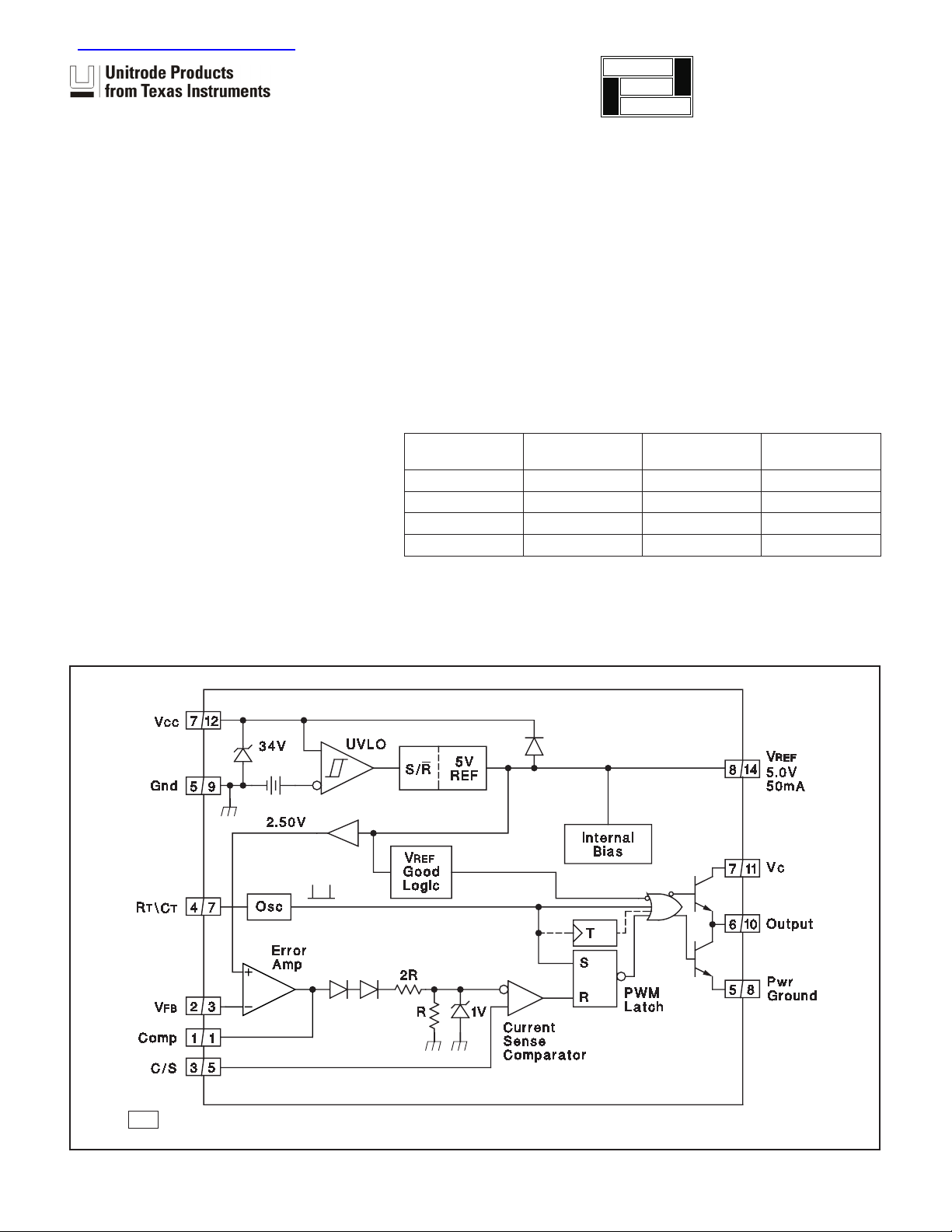
BLOCK DIAGRAM
Note 1: A = DIL-8 Pin Number. B = SO-14 Pin Number.
Note 2: Toggle flip flop used only in 1844A and 1845A.
SLUS224A - SEPTEMBER 1994 - REVISED APRIL 2002
A/B
Page 2
CONNECTION DIAGRAMS
ABSOLUTE MAXIMUM RATINGS (Note 1)
Supply Voltage (Low Impedance Source) . . . . . . . . . . . . . . 30V
Supply Voltage (I
Output Current. . . . . . . . . . . . . . . . . . . . . . . . . . . . . . . . . . .±1A
Output Energy (Capacitive Load). . . . . . . . . . . . . . . . . . . . . 5µJ
Analog Inputs (Pins 2, 3). . . . . . . . . . . . . . . . . . . -0.3V to +6.3V
Error Amp Output Sink Current . . . . . . . . . . . . . . . . . . . . 10mA
Power Dissipation at T
Storage Temperature Range. . . . . . . . . . . . . . -65°C to +150°C
Lead Temperature (Soldering, 10 Seconds) . . . . . . . . . . 300°C
Note 1. All voltages are with respect to Ground, Pin 5. Currents
are positive into, negative out of the specified terminal. Consult
Packaging Section of Databook for thermal limitations and con
siderations of packages. Pin numbers refer to DIL package only.
SOIC-14 (TOP VIEW)
D Package
CC mA) . . . . . . . . . . . . . . . . . . . . Self Limiting
A ≤ 25°C (DIL-8) . . . . . . . . . . . . . . . . 1W
-
PLCC-20, LCC-20
(TOP VIEW)
Q, L Packages
UC1842A/3A/4A/5A
UC2842A/3A/4A/5A
UC3842A/3A/4A/5A
PACKAGE PIN FUNCTION
FUNCTION PIN
N/C
Comp 2
N/C 3-4
VFB 5
N/C 6
ISENSE 7
N/C 8-9
RT/CT 10
N/C 11
Pwr Gnd 12
Gnd 13
N/C 14
Output 15
N/C 16
VC 17
VCC 18
N/C 19
VREF 20
1
SOIC-WIDE16 (TOP VIEW)
DW Package
N/C
1
N/C
2
COMP
ISENSE
RT/CT
VFB
N/C
N/C
3
4
5
6
7
8
16
15
14
13
12
11
10
9
DIL-8, SOIC-8 (TOP VIEW)
J or N, D8 Package
N/C
VREF
VCC
VCC
OUTPUT
GND
PWRGND
N/C
2
Page 3
UC1842A/3A/4A/5A
UC2842A/3A/4A/5A
UC3842A/3A/4A/5A
ELECTRICAL CHARACTERISTICS Unless otherwise stated, these specifications apply for –55°C ≤ TA ≤ 125°C for the
UC184xA; –40°C ≤ T
(Note 5); R
T = 10k; CT = 3.3nF; TA =TJ; Pin numbers refer to DIL-8.
A ≤ 125°C for the UC284xAQ; –40°C ≤ TA ≤ 85°C for the UC284xA; 0 ≤ TA ≤ 70°C for the UC384xA; VCC = 15V
PARAMETER TEST CONDITIONS
UC184xA\UC284xA UC384xA
MIN. TYP. MAX. MIN. TYP. MAX.
UNITS
Reference Section
Output Voltage T
Line Regulation 12 ≤ V
Load Regulation 1 ≤ I
J = 25°C, IO = 1mA 4.95 5.00 5.05 4.90 5.00 5.10 V
IN 25V 6 20 6 20 mV
O ≤ 20mA 6 25 6 25 mV
Temp. Stability (Note 2, Note 7) 0.2 0.4 0.2 0.4 mV/°C
Total Output Variation Line, Load, Temp. 4.9 5.1 4.82 5.18 V
Output Noise Voltage 10Hz ≤ f ≤ 10kHz
J = 25°C (Note 2) 50 50 µV
T
Long Term Stability T
A = 125°C, 1000Hrs. (Note 2) 5 25 5 25 mV
Output Short Circuit -30 -100 -180 -30 -100 -180 mA
Oscillator Section
Initial Accuracy T
Voltage Stability 12 ≤ V
Temp. Stability T
Amplitude V
Discharge Current T
J = 25°C (Note 6) 47 52 57 47 52 57 kHz
CC ≤ 25V 0.2 1 0.2 1 %
MIN ≤ TA ≤ TMAX (Note 2) 5 5 %
PIN 4 peak to peak (Note 2) 1.7 1.7 V
J = 25°C, VPIN 4 = 2V (Note 8) 7.8 8.3 8.8 7.8 8.3 8.8 mA
PIN 4 = 2V (Note 8) 7.5 8.8 7.6 8.8 mA
V
Error Amp Section
Input Voltage V
PIN 1 = 2.5V 2.45 2.50 2.55 2.42 2.50 2.58 V
Input Bias Current -0.3 -1 -0.3 -2
VOL 2 ≤ VO ≤ 4V 65 90 65 90 dB
A
Unity Gain Bandwidth T
PSRR 12 ≤ V
Output Sink Current V
Output Source Current V
OUT High VPIN 2 = 2.3V, RL = 15k to ground 5 6 5 6 V
V
OUT Low VPIN 2 = 2.7V, RL = 15k to Pin 8 0.7 1.1 0.7 1.1 V
V
J = 25°C (Note 2) 0.7 1 0.7 1 MHz
CC ≤ 25V 60 70 60 70 dB
PIN 2 = 2.7V, VPIN 1 = 1.1V 2 6 2 6 mA
PIN 2 = 2.3V, VPIN 1 = 5V -0.5 -0.8 -0.5 -0.8 mA
Current Sense Section
Gain (Note 3, Note 4) 2.85 3 3.15 2.85 3 3.15 V/V
Maximum Input Signal V
PSRR 12 ≤ V
PIN 1 = 5V (Note 3) 0.9 1 1.1 0.9 1 1.1 V
CC ≤ 25V (Note 3) 70 70 dB
Input Bias Current -2 -10 -2 -10
Delay to Output V
PIN 3 = 0 to 2V (Note 2) 150 300 150 300 ns
Output Section
Output Low Level I
Output High Level I
Rise Time T
Fall Time T
UVLO Saturation V
SINK = 20mA 0.1 0.4 0.1 0.4 V
SINK = 200mA 15 2.2 15 2.2 V
I
SOURCE = 20mA 13 13.5 13 13.5 V
SOURCE = 200mA 12 13.5 12 13.5 V
I
J = 25°C, CL = 1nF (Note 2) 50 150 50 150 ns
J = 25°C, CL = 1nF (Note 2) 50 150 50 150 ns
CC = 5V, ISINK = 10mA 0.7 1.2 0.7 1.2 V
A
µ
A
µ
3
Page 4
UC1842A/3A/4A/5A
UC2842A/3A/4A/5A
UC3842A/3A/4A/5A
ELECTRICAL CHARACTERISTICS Unless otherwise stated, these specifications apply for –55°C ≤ TA ≤ 125°C for the
UC184xA; –40°C ≤ T
(Note 5); R
T = 10k; CT = 3.3nF; TA =TJ; Pin numbers refer to DIL-8.
A ≤ 125°C for the UC284xAQ; –40°C ≤ TA ≤ 85°C for the UC284xA; 0 ≤ TA ≤ 70°C for the UC384xA; VCC = 15V
PARAMETER TEST CONDITIONS
UC184xA\UC284xA UC384xA
MIN. TYP. MAX. MIN. TYP. MAX.
UNITS
Under-Voltage Lockout Section
Start Threshold x842A/4A 15 16 17 14.5 16 17.5 V
x843A/5A 7.8 8.4 9.0 7.8 8.4 9.0 V
Min. Operation Voltage After x842A/4A 9 10 11 8.5 10 11.5 V
Turn On x843A/5A 7.0 7.6 8.2 7.0 7.6 8.2 V
PWM Section
Maximum Duty Cycle x842A/3A 94 96 100 94 96 100 %
x844A/5A 47 48 50 47 48 50 %
Minimum Duty Cycle 0 0 %
Total Standby Current
Start-Up Current 0.3 0.5 0.3 0.5 mA
Operating Supply Current V
CC Zener Voltage ICC = 25mA 30 34 30 34 V
V
PIN 2 =VPIN 3 = 0V 11 17 11 17 mA
Note 2: Ensured by design, but not 100% production tested.
Note 3: Parameter measured at trip point of latch with V
VPIN
∆
1
;0
V
Note 4: Gain defined as:
Note 5: Adjust V
CC
above the start threshold before setting at 15V.
A
=
VPIN
∆
3
PIN 3
PIN2
0.8V.
= 0.
Note 6: Output frequency equals oscillator frequency for the UC1842A and UC1843A. Output frequency is one half oscillator frequency for the UC1844A and UC1845A.
Note 7: “Temperature stability, sometimes referred to as average temperature coefficient, is described by the equation:
Temp Stability
VREF max VREF min
=
TJ max TJ min
−
() ()
−
() ()
.V
REF
(max) and V
REF
(min) are the maximum & minimum reference volt-
age measured over the appropriate temperature range. Note that the extremes in voltage do not necessarily occur at the extremes
in temperature.”
Note 8: This parameter is measured with R
The total current flowing into the R
T/Cpin will be approximately 300
T
= 10k to V
REF
.This contributes approximately 300 A of current to the measurement.
A higher than the measured value.
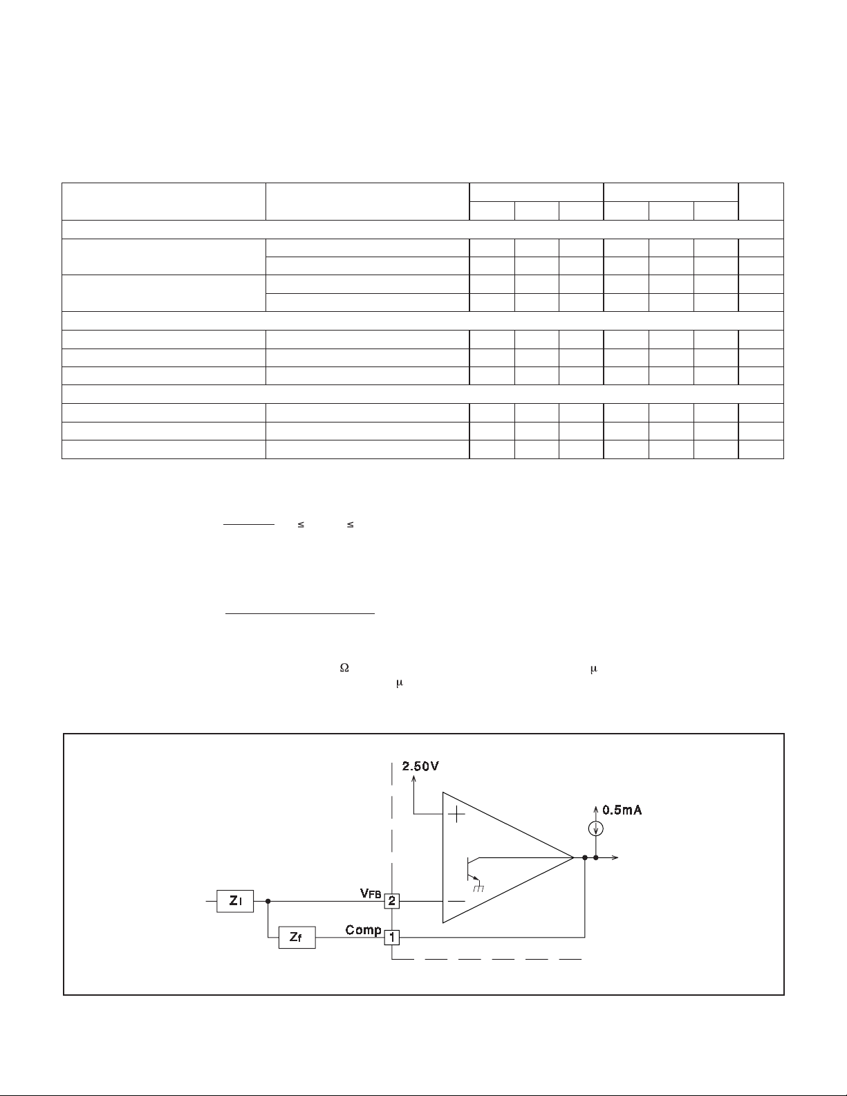
Error Amp Configuration
Error Amp can Source and Sink up to 0.5mA, and Sink up to 2mA.
4
Page 5

Under-Voltage Lockout
Current Sense Circuit
UC1842A/3A/4A/5A
UC2842A/3A/4A/5A
UC3842A/3A/4A/5A
During UVLO, the Output is low.
Peak Current (I
A small RC filter may be required to suppress switch transients.
S) is Determined By The Formula
SMAX ′
I
1.0V
RS
Error Amplifier Open-Loop Frequency ResponseOutput Saturation Characteristics
5
Page 6

APPLICATIONS DATA (cont.)
Oscillator Section
Oscillator Frequency vs Timing Resistance Maximum Duty Cycle vs Timing Resistor
UC1842A/3A/4A/5A
UC2842A/3A/4A/5A
Open-Loop Laboratory Test Fixture
High peak currents associated with capacitive loads necessi
tate careful grounding techniques. Timing and bypass capaci
tors should be connected close to pin 5 in a single point
Slope Compensation
-
ground. The transistor and 5k potentiometer are used to sam
-
ple the oscillator waveform and apply an adjustable ramp to
pin 3.
A fraction of the oscillator ramp can be resistively
summed with the current sense signal to provide slope
compensation for converters requiring duty cycles over
50%.
Note that capacitor, C, forms a filter with R2 to suppress
the leading edge switch spikes.
-
6
Page 7

APPLICATIONS DATA (cont.)
Off-line Flyback Regulator
UC1842A/3A/4A/5A
UC2842A/3A/4A/5A
UC3842A/3A/4A/5A
Power Supply Specifications
1. Input Voltage 95VAC to 130VA
(50 Hz/60Hz)
2. Line Isolation 3750V
3. Switching Frequency 40kHz
4. Efficiency Full Load 70%
5. Output Voltage:
A. +5V,
B. +12V,
C. -12V ,
5%; 1A to 4A load
±
Ripple voltage: 50mV P-P Max
3%; 0.1A to 0.3A load
±
Ripple voltage: 100mV P-P Max
3%; 0.1A to 0.3A load
±
Ripple voltage: 100mV P-P Max
7
Page 8

PACKAGE OPTION ADDENDUM
www.ti.com
PACKAGING INFORMATION
Orderable Device Status
5962-8670405PA ACTIVE CDIP JG 8 1 None A42 SNPB Level-NC-NC-NC
5962-8670405VPA ACTIVE CDIP JG 8 1 None Call TI Level-NC-NC-NC
5962-8670405VXA ACTIVE LCCC FK 20 1 None Call TI Level-NC-NC-NC
5962-8670405XA ACTIVE LCCC FK 20 1 None POST-PLATE Level-NC-NC-NC
5962-8670406PA ACTIVE CDIP JG 8 1 None A42 SNPB Level-NC-NC-NC
5962-8670406VPA ACTIVE CDIP JG 8 1 None Call TI Level-NC-NC-NC
5962-8670406VXA ACTIVE LCCC FK 20 1 None Call TI Level-NC-NC-NC
5962-8670406XA ACTIVE LCCC FK 20 1 None POST-PLATE Level-NC-NC-NC
5962-8670407PA ACTIVE CDIP JG 8 1 None A42 SNPB Level-NC-NC-NC
5962-8670407VPA ACTIVE CDIP JG 8 1 None Call TI Level-NC-NC-NC
5962-8670407VXA ACTIVE LCCC FK 20 1 None Call TI Level-NC-NC-NC
5962-8670407XA ACTIVE LCCC FK 20 1 None POST-PLATE Level-NC-NC-NC
5962-8670408PA ACTIVE CDIP JG 8 1 None A42 SNPB Level-NC-NC-NC
5962-8670408VPA ACTIVE CDIP JG 8 1 None Call TI Level-NC-NC-NC
5962-8670408VXA ACTIVE LCCC FK 20 1 None Call TI Level-NC-NC-NC
5962-8670408XA ACTIVE LCCC FK 20 1 None POST-PLATE Level-NC-NC-NC
UC1842AJ ACTIVE CDIP JG 8 1 None A42 SNPB Level-NC-NC-NC
UC1842AJ883B ACTIVE CDIP JG 8 1 None A42 SNPB Level-NC-NC-NC
UC1842AJQMLV ACTIVE CDIP JG 8 None CallTI Call TI
UC1842AL883B ACTIVE LCCC FK 20 1 None POST-PLATE Level-NC-NC-NC
UC1842ALQMLV ACTIVE LCCC FK 20 None Call TI Call TI
UC1843AJ ACTIVE CDIP JG 8 1 None A42 SNPB Level-NC-NC-NC
UC1843AJ883B ACTIVE CDIP JG 8 1 None A42 SNPB Level-NC-NC-NC
UC1843AJQMLV ACTIVE CDIP JG 8 None Call TI Call TI
UC1843AL883B ACTIVE LCCC FK 20 1 None POST-PLATE Level-NC-NC-NC
UC1843ALQMLV ACTIVE LCCC FK 20 None Call TI Call TI
UC1844AJ ACTIVE CDIP JG 8 1 None A42 SNPB Level-NC-NC-NC
UC1844AJ883B ACTIVE CDIP JG 8 1 None A42 SNPB Level-NC-NC-NC
UC1844AJQMLV ACTIVE CDIP JG 8 None Call TI Call TI
UC1844AL883B ACTIVE LCCC FK 20 1 None POST-PLATE Level-NC-NC-NC
UC1844ALQMLV ACTIVE LCCC FK 20 None Call TI Call TI
UC1845AJ ACTIVE CDIP JG 8 1 None A42 SNPB Level-NC-NC-NC
UC1845AJ883B ACTIVE CDIP JG 8 1 None A42 SNPB Level-NC-NC-NC
UC1845AJQMLV ACTIVE CDIP JG 8 None Call TI Call TI
UC1845AL883B ACTIVE LCCC FK 20 1 None POST-PLATE Level-NC-NC-NC
UC1845ALQMLV ACTIVE LCCC FK 20 None Call TI Call TI
UC2842AD ACTIVE SOIC D 14 50 None CU NIPDAU Level-1-220C-UNLIM
UC2842AD8 ACTIVE SOIC D 8 75 None CU NIPDAU Level-1-220C-UNLIM
UC2842AD8TR ACTIVE SOIC D 8 2500 None CU NIPDAU Level-1-220C-UNLIM
UC2842AD8TRG4 ACTIVE SOIC D 8 2500 None CallTI Call TI
UC2842ADTR ACTIVE SOIC D 14 2500 None CU NIPDAU Level-1-220C-UNLIM
UC2842ADW ACTIVE SOIC DW 16 40 None CU NIPDAU Level-2-220C-1 YEAR
(1)
Package
Type
Package
Drawing
Pins Package
Qty
Eco Plan
(2)
Lead/Ball Finish MSL Peak Temp
10-Mar-2005
(3)
Addendum-Page 1
Page 9

PACKAGE OPTION ADDENDUM
www.ti.com
Orderable Device Status
(1)
Package
Type
Package
Drawing
Pins Package
Qty
Eco Plan
(2)
Lead/Ball Finish MSL Peak Temp
10-Mar-2005
UC2842ADWTR ACTIVE SOIC DW 16 2000 None CU NIPDAU Level-2-220C-1 YEAR
UC2842AJ OBSOLETE CDIP JG 8 None Call TI Call TI
UC2842AN ACTIVE PDIP P 8 50 Pb-Free
CU SNPB Level-NC-NC-NC
(RoHS)
UC2843AD ACTIVE SOIC D 14 50 None CU NIPDAU Level-1-220C-UNLIM
UC2843AD8 ACTIVE SOIC D 8 75 None CU NIPDAU Level-1-220C-UNLIM
UC2843AD8TR ACTIVE SOIC D 8 2500 None CU NIPDAU Level-1-220C-UNLIM
UC2843ADTR ACTIVE SOIC D 14 2500 None CU NIPDAU Level-1-220C-UNLIM
UC2843ADW ACTIVE SOIC DW 16 40 None CU NIPDAU Level-2-220C-1 YEAR
UC2843ADWTR ACTIVE SOIC DW 16 2000 None CU NIPDAU Level-2-220C-1 YEAR
UC2843AJ OBSOLETE CDIP JG 8 None Call TI Call TI
UC2843AN ACTIVE PDIP P 8 50 Pb-Free
CU SNPB Level-NC-NC-NC
(RoHS)
UC2843AQ ACTIVE PLCC FN 20 46 None CU SNPB Level-2-220C-1 YEAR
UC2844AD ACTIVE SOIC D 14 50 None CU NIPDAU Level-1-220C-UNLIM
UC2844AD8 ACTIVE SOIC D 8 75 None CU NIPDAU Level-1-220C-UNLIM
UC2844AD8TR ACTIVE SOIC D 8 2500 None CU NIPDAU Level-1-220C-UNLIM
UC2844AD8TRG4 PREVIEW SOIC D 8 2500 None Call TI Call TI
UC2844ADTR ACTIVE SOIC D 14 2500 None CU NIPDAU Level-1-220C-UNLIM
UC2844ADW ACTIVE SOIC DW 16 40 None CU NIPDAU Level-2-220C-1 YEAR
UC2844ADWTR ACTIVE SOIC DW 16 2000 None CU NIPDAU Level-2-220C-1 YEAR
UC2844AJ ACTIVE CDIP JG 8 1 None A42 SNPB Level-NC-NC-NC
UC2844AN ACTIVE PDIP P 8 50 Pb-Free
CU SNPB Level-NC-NC-NC
(RoHS)
UC2844AQD ACTIVE SOIC D 14 50 None Call TI Level-1-220C-UNLIM
UC2844AQD8 ACTIVE SOIC D 8 75 None Call TI Level-1-220C-UNLIM
UC2844AQD8R ACTIVE SOIC D 8 2500 None Call TI Level-1-220C-UNLIM
UC2844AQDR ACTIVE SOIC D 14 2500 None Call TI Level-1-220C-UNLIM
UC2845AD ACTIVE SOIC D 14 50 None CU NIPDAU Level-1-220C-UNLIM
UC2845AD8 ACTIVE SOIC D 8 75 None CU NIPDAU Level-1-220C-UNLIM
UC2845AD8TR ACTIVE SOIC D 8 2500 None CU NIPDAU Level-1-220C-UNLIM
UC2845AD8TRG4 PREVIEW SOIC D 8 2500 None Call TI Call TI
UC2845ADTR ACTIVE SOIC D 14 2500 None CU NIPDAU Level-1-220C-UNLIM
UC2845ADW ACTIVE SOIC DW 16 40 None CU NIPDAU Level-2-220C-1 YEAR
UC2845AN ACTIVE PDIP P 8 50 Pb-Free
CU SNPB Level-NC-NC-NC
(RoHS)
UC3842AD ACTIVE SOIC D 14 50 None CU NIPDAU Level-1-220C-UNLIM
UC3842AD8 ACTIVE SOIC D 8 75 None CU NIPDAU Level-1-220C-UNLIM
UC3842AD8TR ACTIVE SOIC D 8 2500 None CU NIPDAU Level-1-220C-UNLIM
UC3842ADTR ACTIVE SOIC D 14 2500 None CU NIPDAU Level-1-220C-UNLIM
UC3842ADW ACTIVE SOIC DW 16 40 None CU NIPDAU Level-2-220C-1 YEAR
UC3842ADWTR ACTIVE SOIC DW 16 2000 None CU NIPDAU Level-2-220C-1 YEAR
UC3842AJ ACTIVE CDIP JG 8 1 None A42 SNPB Level-NC-NC-NC
UC3842AN ACTIVE PDIP P 8 50 Pb-Free
CU SNPB Level-NC-NC-NC
(RoHS)
(3)
Addendum-Page 2
Page 10

PACKAGE OPTION ADDENDUM
www.ti.com
Orderable Device Status
(1)
Package
Type
Package
Drawing
Pins Package
Qty
Eco Plan
UC3842ANG4 ACTIVE PDIP P 8 50 Green (RoHS &
(2)
Lead/Ball Finish MSL Peak Temp
CU NIPDAU Level-NA-NA-NA
10-Mar-2005
(3)
no Sb/Br)
UC3843AD ACTIVE SOIC D 14 50 None CU NIPDAU Level-1-220C-UNLIM
UC3843AD8 ACTIVE SOIC D 8 75 None CU NIPDAU Level-1-220C-UNLIM
UC3843AD8G4 ACTIVE SOIC D 8 75 None Call TI Call TI
UC3843AD8TR ACTIVE SOIC D 8 2500 None CU NIPDAU Level-1-220C-UNLIM
UC3843AD8TRG4 ACTIVE SOIC D 8 2500 Green (RoHS &
CU NIPDAU Level-1-260C-UNLIM
no Sb/Br)
UC3843ADG4 ACTIVE SOIC D 14 50 Green (RoHS &
CU NIPDAU Level-1-260C-UNLIM
no Sb/Br)
UC3843ADTR ACTIVE SOIC D 14 2500 None CU NIPDAU Level-1-220C-UNLIM
UC3843AJ ACTIVE CDIP JG 8 1 None A42 SNPB Level-NC-NC-NC
UC3843AN ACTIVE PDIP P 8 50 Pb-Free
CU SNPB Level-NC-NC-NC
(RoHS)
UC3843ANG4 ACTIVE PDIP P 8 50 Green (RoHS &
CU NIPDAU Level-NA-NA-NA
no Sb/Br)
UC3844AD ACTIVE SOIC D 14 50 None CU NIPDAU Level-1-220C-UNLIM
UC3844AD8 ACTIVE SOIC D 8 75 None CU NIPDAU Level-1-220C-UNLIM
UC3844AD8TR ACTIVE SOIC D 8 2500 None CU NIPDAU Level-1-220C-UNLIM
UC3844AD8TRG4 ACTIVE SOIC D 8 2500 Green (RoHS &
CU NIPDAU Level-1-260C-UNLIM
no Sb/Br)
UC3844ADTR ACTIVE SOIC D 14 2500 None CU NIPDAU Level-1-220C-UNLIM
UC3844ADW ACTIVE SOIC DW 16 40 None CU NIPDAU Level-2-220C-1 YEAR
UC3844ADWTR ACTIVE SOIC DW 16 2000 None CU NIPDAU Level-2-220C-1 YEAR
UC3844AN ACTIVE PDIP P 8 50 Pb-Free
CU SNPB Level-NC-NC-NC
(RoHS)
UC3845AD ACTIVE SOIC D 14 50 None CU NIPDAU Level-1-220C-UNLIM
UC3845AD8 ACTIVE SOIC D 8 75 None CU NIPDAU Level-1-220C-UNLIM
UC3845AD8TR ACTIVE SOIC D 8 2500 None CU NIPDAU Level-1-220C-UNLIM
UC3845ADTR ACTIVE SOIC D 14 2500 None CU NIPDAU Level-1-220C-UNLIM
UC3845ADW ACTIVE SOIC DW 16 40 None CU NIPDAU Level-2-220C-1 YEAR
UC3845ADWTR ACTIVE SOIC DW 16 2000 None CU NIPDAU Level-2-220C-1 YEAR
UC3845AJ ACTIVE CDIP JG 8 1 None A42 SNPB Level-NC-NC-NC
UC3845AN ACTIVE PDIP P 8 50 Pb-Free
CU SNPB Level-NC-NC-NC
(RoHS)
UC3845ANG4 ACTIVE PDIP P 8 50 Green (RoHS &
CU NIPDAU Level-NA-NA-NA
no Sb/Br)
(1)
The marketing status values are defined as follows:
ACTIVE: Product device recommended for new designs.
LIFEBUY: TI has announced that the device will be discontinued, and a lifetime-buy period is in effect.
NRND: Not recommended for new designs. Device is in production to support existing customers, but TI does not recommend using this part in
a new design.
PREVIEW: Device has been announced but is not in production. Samples may or may not be available.
OBSOLETE: TI has discontinued the production of the device.
(2)
Eco Plan - May not be currently available - please check http://www.ti.com/productcontent for the latest availability information and additional
product content details.
None: Not yet available Lead (Pb-Free).
Pb-Free (RoHS): TI's terms "Lead-Free" or "Pb-Free" mean semiconductor products that are compatible with the current RoHS requirements
Addendum-Page 3
Page 11

PACKAGE OPTION ADDENDUM
www.ti.com
for all 6 substances, including the requirement that lead not exceed 0.1% by weight in homogeneous materials. Where designed to be soldered
at high temperatures, TI Pb-Free products are suitable for use in specified lead-free processes.
Green (RoHS & no Sb/Br): TI defines "Green" to mean "Pb-Free" and in addition, uses package materials that do not contain halogens,
including bromine (Br) or antimony (Sb) above 0.1% of total product weight.
(3)
MSL, Peak Temp. -- The Moisture Sensitivity Level rating according to the JEDECindustry standard classifications, and peak solder
temperature.
Important Information and Disclaimer:The information provided on this page represents TI's knowledge and belief as of the date that it is
provided. TI bases its knowledge and belief on information provided by third parties, and makes no representation or warranty as to the
accuracy of such information. Efforts are underway to better integrate information from third parties. TI has taken and continues to take
reasonable steps to provide representative and accurate information but may not have conducted destructive testing or chemical analysis on
incoming materials and chemicals. TI and TI suppliers consider certain information to be proprietary, and thus CAS numbers and other limited
information may not be available for release.
In no event shall TI's liability arising out of such information exceed the total purchase price of the TI part(s) at issue in this document sold by TI
to Customer on an annual basis.
10-Mar-2005
Addendum-Page 4
 Loading...