

Programmable, Off-Line, PWM Controller
DESCRIPTI ONFEATURES
• All Control, Driving, Monitoring, and
Protection Functions Included
• Low-current, Off-line Start Circuit
• Voltage Feed Forward or Current
Mode Control
• Guaranteed Duty Cycle Clamp
• PWM Latch for Single Pulse per Period
• Pulse-by-Pulse Current Limiting Plus
Shutdown for Over-Current Fault
• No Start-up or Shutdown Transients
• Slow Turn-on Both Initially and After
Fault Shutdown
• Shutdown Upon Over- or
Under-Voltage Sensing
• Latch Off or Continuous Retry After
Fault
• PWM Output Switch Usable to 1A
Peak Current
• 1% Reference Accuracy
• 500kHz Operation
• 18 Pin DIL Package
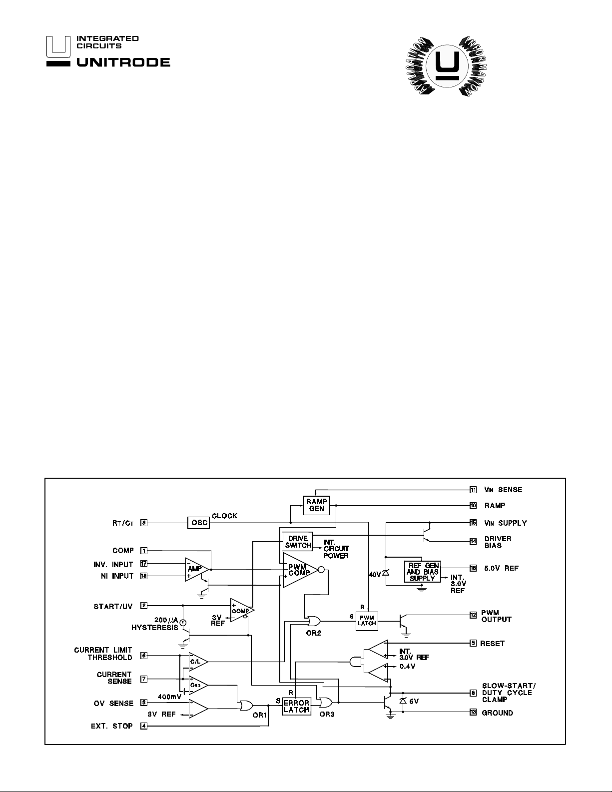
BLOCK DIAGRA M
The UC1841 family of PWM controllers has been designed to increase
the level of versatility while retaining all of the performance features of
the earlier UC18 40 de vices. While still optimized for highly-efficient bootstrapped pri mary-side operati on in forward or flyback power converters,
the UC1841 is equall y adept in impl ementing b oth low a nd high voltage
input DC to DC converters. Important performance features include a
low-current starting circuit, linear feed-forward for constant volt-second
operation, and compatibility with either voltage or current mode topologies.
In addition to start-up and normal regulating PWM functions, these devices include built in protection from over-voltage, under-voltage, and
over-current fault conditions with the option for either latch-of f or automatic restart.
While pin compatib le with the UC1840 in all respects except that the polarity of the External Stop has bee n re versed, the UC1841 offers the following improvements:
1. Fault latch reset is accomplished with slow start discharge rather
than recycling the input voltage to the chip.
2. The External Stop input can be used for a fault delay to resist
shutdown from short durat ion transients.
3. The duty-cycle clamping function has been characterized an d
specified.
The UC1841 is characteri zed for -55°C to +125°C operation while the
UC2841 and UC3841 are desi gned for -25°C to +85°C and 0°to +70°C,
respectively.
UC1841
UC2841
UC3841
Note: Positive tru e lo gic, latch output s high wit h set, reset has prior ity.
6/93
ABSOLUTE MAXI MUM RATING S
Supply Voltage, +VIN (Pin 15) (Note 2)
Voltage Driven. . . . . . . . . . . . . . . . . . . . . . . . . . . . . . . . . +32V
Current Drive n, 100mA maximum. . . . . . . . . . . . Self-limiting
PWM Output Volta ge (Pin 12 ) . . . . . . . . . . . . . . . . . . . . . . . 40V
PWM Out put Current, Steady-State (Pin 12). . . . . . . . . 400mA
PWM Output Peak Energy Disc harge . . . . . . . . . . . . 20 µJo ules
Driver Bias Current (Pin 14). . . . . . . . . . . . . . . . . . . . . -200mA
Reference Output Current (Pin 16) . . . . . . . . . . . . . . . . -50mA
Slow-Start Sink Curren t (Pin 8) . . . . . . . . . . . . . . . . . . . . 20mA
V
IN Sense Current (Pin 11). . . . . . . . . . . . . . . . . . . . . . . . 10mA
Current Limit Input s (Pins 6 & 7) . . . . . . . . . . . . . -0.5 to +5.5V
Stop Input (Pin 4) . . . . . . . . . . . . . . . . . . . . . . . . . -0.3 to +5. 5V
Compara to r Inputs
(Pins 1, 7, 9-1 1, 1 6). . . . . . . . . . . . Internally clamp ed at 12V
Power Dissipation at T
Power Dissipation at T
A = 25°C (Note 3) . . . . . . . . . . . 1000mW
C = 25°C (Note 3). . . . . . . . . . . 2000mW
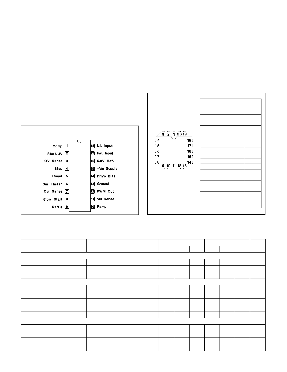
CONNECTION DIAGRAMS
DIL-18, SOIC- 18 (T O P VIEW)
J or N, DW Package
UC1841
UC2841
UC3841
Operating Junct ion Te mp era tu re . . . . . . . . . . -55°C to +150°C
Storage Temperature Range. . . . . . . . . . . . . . -65°C to +150°C
Lead Temp era ture (Solder in g, 10 sec). . . . . . . . . . . . . +300°C
Note 1: All voltages are with respect to ground, Pin 13.
Currents are positiv e-int o, negat ive-o ut of the specif ie d
terminal.
Note 2: All p in num ber s are refer ence d to DIL- 18 pa ckag e.
Note 3: C on sult Packag in g Section of Dat aboo k for ther ma l
limitations and cons id era tion s of packa ge.
PLCC-20, LCC-20
(TOP VIEW)
Q or L Package
PACKAGE PIN FUNCTIONS
FUNCTION PIN
Comp 1
Start/UV 2
OV Sense 3
Stop 4
Reset 5
CUR Thresh 7
CUR Sense 8
Slow Start 9
R
T/CT 10
Ramp 11
V
IN Sense 12
PWM Out 13
Ground 14
Drive Bias 15
+V
IN Supply 17
5.0V REF 18
Inv. Input 19
N.I. Inpu t 20
ELECTRICAL CHARACTERISTICS:
UC1841, -25°C to +85°C for the UC2841, and 0°C to +70 °C for the UC3841; V
C
R = .001mfd, Current Lim it Thres hold = 200 mV, TA = TJ.
Unless otherwise stated , these spec ificat ions apply for TA = -55°C to +125°C for the
IN = 20V, RT = 20k Ω , CT = .001mfd, RR = 10kΩ,
UC1841 / UC2841 UC3841 UNITS
PARAMETER TEST CONDITIONS
MIN TYP MAX MIN TYP MAX
Power Inputs
Start-Up Curr ent V
Operating Cur ren t V
Supply OV Clamp I
IN = 30V, Pin 2 = 2.5V 4.5 6 4.5 6 mA
IN = 30V, Pin 2 = 3.5V 10 14 10 14 mA
IN = 20mA 33 40 45 33 40 45 V
Reference Sec tio n
Reference Voltage T
Line Regulatio n V
Load Regulation I
J = 25°C 4.95 5.0 5.05 4.9 5.0 5.1 V
IN = 8 to 30V 10 15 10 20 mV
L = 0 to 10mA 1020 1030mV
Temperature Stability Over Operating Temper ature Range 4.9 5.1 4 .8 5 5.15 V
Short Circuit Current V
REF = 0, TJ
= 25°C -80 -100 -80 -100 mA
Oscillator
J
Nominal Frequency T
Voltage Stability V
= 25°C 47 50 53 45 50 55 kHz
IN = 8 to 30V 0.5 1 0.5 1 %
Temperature Stability Over Operating Temper ature Range 45 55 43 57 kHz
Maximum Frequency R
T = 2kΩ, CT = 330pF 500 500 kHz
2
ELECTRICAL CHARACTERISTICS:
UC1841, -25°C to +85°C for the UC2841, and 0°C to +70 °C for the UC3841; V
C
R = .001mfd, Current Limit Thresh old = 200mV, TA = TJ.
Unless otherwise stated , these spec ificat ions apply for TA = -55°C to +125°C for the
IN = 20V, RT = 20k Ω , CT = .001mfd, RR = 10kΩ,
PARAMETER TEST CONDITIONS UC1841 / UC2841 UC3841 UNITS
MIN TYP MAX MIN TYP MAX
Ramp Ge nerator
Ramp Curren t, M in imum I
Ramp Current, M axim um I
SENSE = -10µA -11 -14 -11 -14 µA
SENSE = 1.0mA -0.9 -.95 -0.9 -.95 mA
Ramp Valley 0.3 0.4 0.6 0.3 0.4 0.6 V
Ramp Peak Clamp ing Leve l 3.9 4.2 4.5 3.9 4.2 4.5 V
Error Amplifier
Input Offs et Vo lta ge V
CM = 5.0V 0.5 5 2 10 mV
Input Bias Cur rent 0.5 2 1 5 µA
Input Offs et Cu rr ent 0.5 0.5 µA
Open Loop Gain ∆V
Output Swing (Max. Output ≤
O= 1 to 3V 60 66 60 66 dB
Minimum Total Range 0.3 3.5 0.3 3.5 V
Ramp Peak - 100mV)
CMRR V
PSRR V
Short Circuit Current V
Gain Bandwidth* T
Slew Rate* T
CM = 1.5 to 5.5V 70 80 70 80 dB
IN = 8 to 30V 70 80 70 80 dB
COMP = 0V -4 -10 -4 -10 mA
J = 25°C, AVOL = 0dB 1 2 1 2 MHz
J = 25°C, AVCL
= 0dB 0.8 0.8 V/µs
PWM Section
Continuous Duty Cycle
Range* (other than zero)
50% Duty Cycle Clamp R
Output Saturation I
Output Lea kage V
Comparator Dela y* Pin 8 to Pin 12, T
Minimum Total Cont inuou s Range,
495495%
Ramp Peak < 4.2V
SENSE to VREF = 10k 42 47 52 42 47 52 %
OUT = 20mA 0.2 0.4 0.2 0.4 V
I
OUT = 200mA 1. 7 2. 2 1.7 2.2 V
OUT = 40V 0.1 10 0. 1 10 µA
J = 25°C, RL = 1kΩ 300 500 300 500 ns
Sequencing Functions
Comparator Thre sholds P ins 2, 3, 5 2.8 3.0 3.2 2.8 3.0 3.2 V
Input Bias Curren t Pins 3, 5 = 0V -1.0 -4.0 -1.0 -4.0 µA
Input Leakage Pins 3, 5 = 10V 0.1 2.0 0.1 2.0 µA
Start/UV Hyster esis Cur ren t Pin 2 = 2.5V 170 200 220 1 70 200 23 0 µA
Ext. Stop Threshold Pin 4 0.8 1.6 2.4 0.8 1.6 2.4 V
Error Latch Activat e Cur ren t Pin 4 = 0V, Pin 3 > 3V -120 -20 0 -120 -20 0 µA
Driver Bias Saturation Volta ge,
V
IN - VOH
Driver Bias Leakage V
Slow-Start Saturation I
Slow-Start Leakage V
IB = -50mA 2 3 2 3 V
B = 0V -0.1 -10 -0.1 -10 µA
S = 10mA 0.2 0.5 0.2 0.5 V
S = 4.5V 0.1 2.0 0.1 2.0 µA
Current Control
Current Limit Off set 0 5 0 10 mV
Current Shutdown O ffs et 370 400 430 360 400 440 mV
Input Bias Current Pin 7 = 0V -2 -5 -2 -5 µA
Common Mode Range* -0.4 3.0 -0.4 3.0 V
Current Limit Delay* T
J = 25°C, Pin 7 to 12, RL = 1k 200 400 200 400 ns
* These paramet ers are guara nt eed by design bu t not 100% teste d in prod uct ion.
UC1841
UC2841
UC3841
3

FUNCTIONAL DES CRIP TIO N
PWM CONTROL
1. Oscillator Gen era te s a fixed-frequency int er nal clock fro m an extern al R
K
Frequency =
C
where KC is a first order correction factor ≈ 0.3 log (CT X 1012).
RTCT
UC1841
UC2841
UC3841
T and CT.
2. Ramp Gener ator
Develops a linear ramp with a slope defined exter nally by
dv
dt
=
sense
R
voltage
RCR
CR is normally se le ct ed ≤ CT and its value will have some effect upon va lley volta ge.
Limiting the minimum value for I
C
R terminal can be used as an input port for curren t mode cont rol.
SENSE will establish a maximum duty cycle clamp .
3. Error Amplifier Conventional operation al amp lifier f or closed- loop ga in and phase com pe nsat ion.
Low output impedance; unity-gain stable.
The output is held low by the slow star t voltag e at turn on in order to minimize over shoo t.
4. Reference Ge n era tor Precision 5.0V for internal and extern al usage to 50mA.
Tracking 3.0V ref er enc e for intern al usage only w ith nomina l accur acy of
± 2%.
40V clamp zener for chip OV prot ect ion, 100m A m axim um current .
5. PWM Comparat or Gen era tes out put pulse which start s at term inat ion of clock pulse and ends whe n the ram p
input crosses the lowest of two posit iv e input s.
6. PWM Latch Terminat es the PW M output pulse whe n set by inputs fro m either th e PWM com pa rator , the
pulse-by-p ulse cur re nt limit compa rator , or the error latch. Reset s with each inter nal clock
pulse.
7. PWM Output Switch Transisto r capable of sinking cu rrent to ground which is of f during the PWM on- tim e and turns
on to terminate the power pulse. Curr ent cap acit y is 400mA sat ur ated with peak
capacitanc e discharge in excess of one am p.
SEQUENCING FUNCTIONS
1. Start/UV Sense With an increasing vo lta g e, it gene rates a turn-on signa l an d releases t he slow- star t clamp at
a start threshold.
With a decreasing volta ge, it genera tes a turn- of f com mand at a lower leve l separ at ed by a
200
µA hystere sis cur ren t.
2. Drive Switch Disab le s most of the chip to hold internal curre nt consump tion low, and Driver Bias OF F, unt il
input voltage reaches start threshold.
3. Driver Bias Supplies drive current to exter nal power switch to prov ide tu rn-on bias .
4. Slow Start Clamps low to hold PWM OFF. Upon release, rises with rate contro lled by R
SCS for slow
increase of output pulse widt h.
Can also be used as an alt ernate maximum duty cycle clamp wit h an ext er nal volt age divider.
PROTECTION FUNCTIO NS
1. Error Latch When set by mome nt ary input , this latch insur es im me diat e PWM shu tdown and hold of f until
reset. Inputs to Error Latch are :
a. OV > 3.2V (typically 3V)
b. Stop > 2.4V (typically 1.6V)
c. Current Sense 400mV ov er thresho ld (typical) .
Error Latch reset s whe n slow start voltage falls to 0.4V if Rese t Pin 5 < 2.8V. Wit h Pin 5 >
3.2V, Error Latch will remain set.
2. Current Limiting Differential input comparator terminat es individual output pulses each t ime sense voltage
rises above thre shold.
When sense volta ge rise s to 400m V (typica l) abov e thres hold, a shutdo wn signal is sent t o
Error Latch.
3. External Stop A voltage over 1.2 V will set the Erro r Latch and hold the ou tp ut off.
A voltage less than 0. 8V w ill defe a t the error latch and prevent shutd o wn.
A capacitor here will slow the action of the erro r latch for tra nsient prot ection by providing a
typical delay of 13ms/
µF.
4
UC1841
UC2841
UC3841
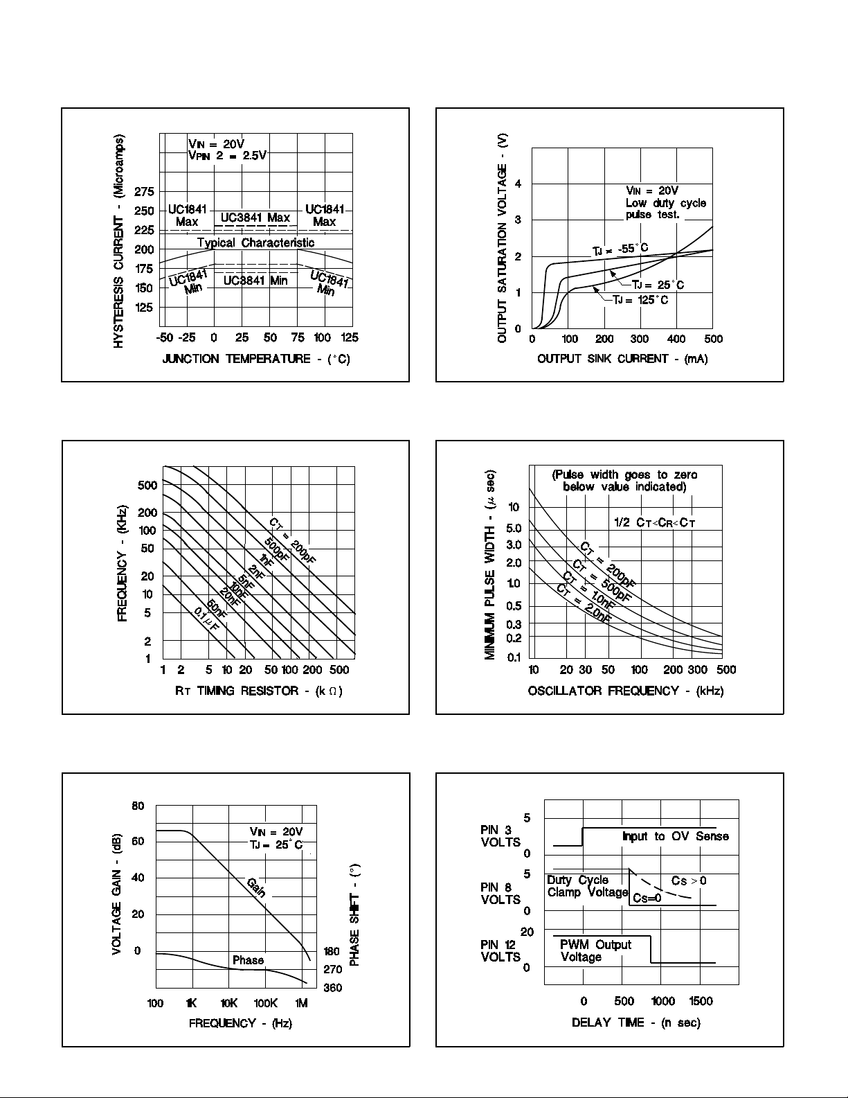
Start/UV Hysteresis
PWM Output-Saturation Voltage
PWM Output Minimu m Pu lse W idthOscillator Frequency
Shutdown TimingError Amplifier Op en Loop Gain an d Phase
5

OPEN-LOOP TEST CIRCUIT
UC1841
UC2841
UC3841
R1
1
= 50 kHz
TCT
R
+ R2 + R3
R2 + R3
+0.2R1 = 12V
UV Fault V olt age = 3
OV Fault V olt age = 3
Nominal Frequency =
Start Voltage = 3
FLYBACK APPLICATION (A)
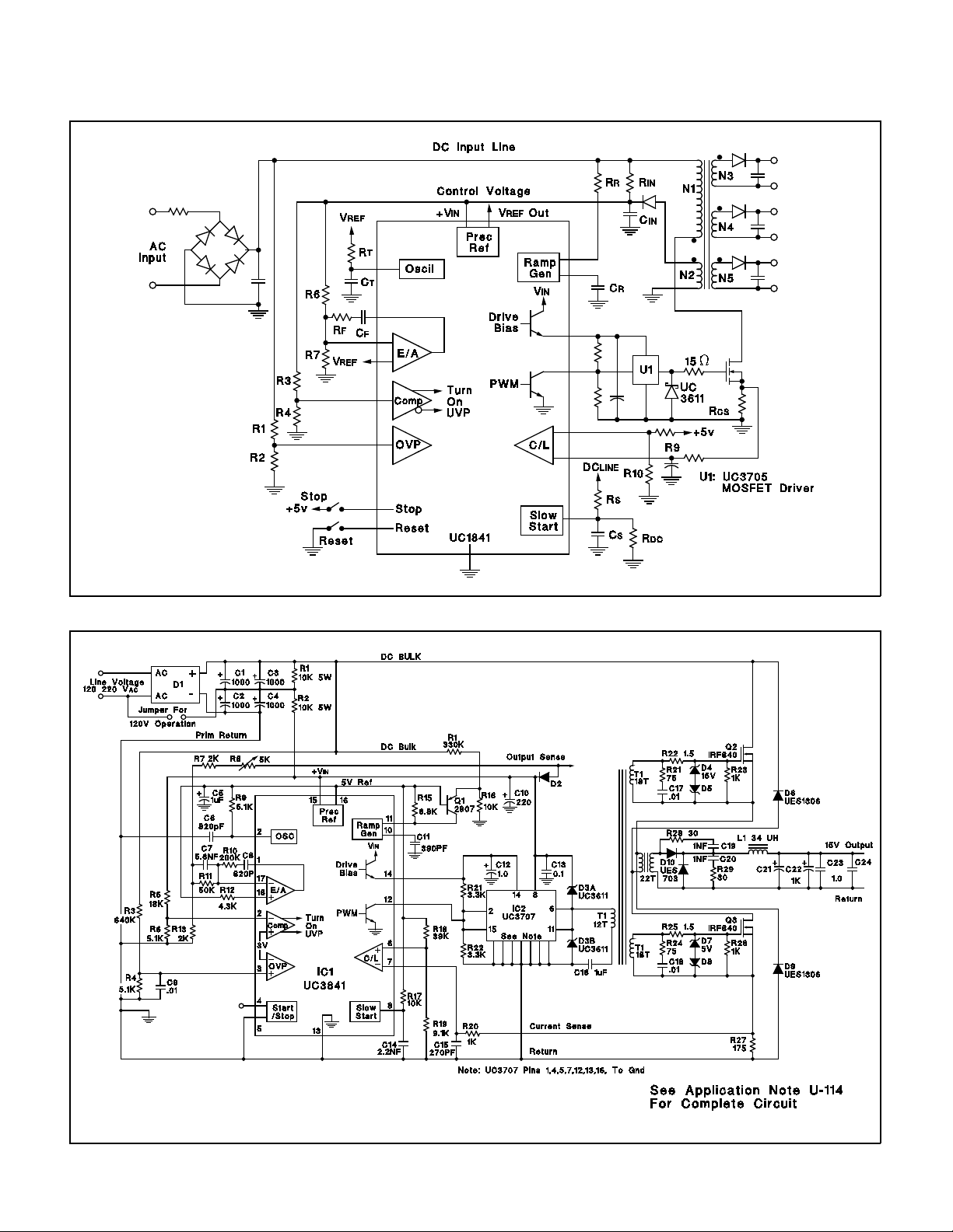
In this application (see Figure A, next page), complete
control is maintained on the primary side. Control power
is provide d by R
IN and CIN during start-up, and by a pri-
mary-referenced low voltage winding, N2, for efficient operation after start. The error amplifier loop is closed to
regulate the DC voltage from N2 with other outputs following through their magnetic coupling − a task made
even easier with the UC1841’s feed−forward line regula-
tion.
An extension t o this application for more precise regulation would be the use of the UC1901 Isolated Feedback
Generator for direct closed-loop control to an output .
R1
R1
+ R2 + R3
R2 + R3
+ R2 + R3
R3
= 8V
= 32V
Curren t Lim it = 20 0mV
Current Fault Voltage = 600mV
Duty Cycle Clamp = 50%
Not shown, are protective snubbers or additional interface
circuitry which may be required by the choice of the highvoltage switch, Qs, or the application; however, one example of power transistor interfacing is provided on the
following page.
REGULATOR APP LI C ATION (B)
With the addition of a level shifting transistor, Q1, the
UC1841 is an ideal control circuit for DC to DC converters
such as the buck regulator shown in Figure B opposite. In
addition t o providin g constant current drive pulses to the
PIC661 power switch, this circuit has full fault protection
and high speed dynamic line regulation due to its feedforward capability. An additional feature is the ability to
6
UC1841
UC2841
UC3841
Figure A. UC1841 Programma ble PW M Cont roller In A Simplified Flyback Regulator
Figure B. Overall Schematic For A 300 Watt, Off -line Power Converter Using The UC 3 841 For Control
7

UC1841
UC2841
UC3841
ERROR LATCH INTERNAL CIRCUITRY
The Error Latch consists of Q5 and Q6 which, when both on,
turns off the PWM Output and pulls the Slow-Start pin low . This
latch is set by either the Over-Voltage or Current Shutdown
comparators, or by a high signal on Pin 4. Reset is accomplished by either the Reset comparator or a low signal on Pin
4. An activation time delay can be provided with an external
capacitor on Pin 4 in conjunction with the ≈ 100µA collector
current from Q4.
CURRENT MODE CONTROL
PROGRAMMABLE SOFT START AND
RESTART DELAY CIRCUIT
VOLTAGE FEED-FO RWARD COMBINED WITH
MAXIMUM DUTY-CYCLE CLAMP
Since Pin 10 is a direct input to the PWM comparator, this
point can also serve as a current sense port for current mode
control. In this application, current sensing is ground referenced through R
R2 (assuming R2 > R
CS. Resistor R1 sets a 400mV offset across
CS) so that both the Error Amplifier and
Fault Shutdown can force the current complete ly to zero. R2 is
also used along with C
F as a small filter to attenuate leading-
edge spikes on the load current waveform. In this mode,
current limiting can be accomplished by divider R3/R4 which
forms a clamp o ver riding the output of the Erro r Amplifier.
UNITRODE INTEGRATED CIRCUITS
7 CONTINENTAL BLVD. • MERRIMACK, NH 03054
TEL. (603) 424-2410 • FAX (603) 424-3460
In this circuit, R1 is used in conjunction with C
R (not shown) to
establish a minimum ramp charging current such that the ramp
voltage reaches 4.2V at the required maximum output pulse
width.
The purpose of Q1 is to provide an increasing ramp current
above a threshold established by R2 and R3 such that the d ut y
cycle is further reduc ed with increa sing VIN.
The minimum ramp current is:
R(MIN) =
l
REF − VIN SENSE
R1
≈
4
R1
V
V
The threshold where VIN begins to add extra ramp curren t is:
R2 + R3R3
IN ≈ 5.6V
V
Above the threshold, the ramp curr ent will be:
l
R (VARIAB ) ≈
4
R1
+
R2
−
5.6
R3
VIN − 5.6
8

PACKAGE OPTION ADDENDUM
www.ti.com
to Customer on an annual basis.
27-Sep-2005
Addendum-Page 2

PACKAGE OPTION ADDENDUM
www.ti.com
19-Jun-2007
PACKAGING INFORMATION
Orderable Device Status
(1)
Package
Type
Package
Drawing
Pins Package
Qty
Eco Plan
5962-8992002VA OBSOLETE CDIP J 18 TBD Call TI Call TI
UC1841J OBSOLETE CDIP J 18 TBD Call TI Call TI
UC1841J883B OBSOLETE CDIP J 18 TBD Call TI Call TI
UC1841L OBSOLETE LCCC FK 20 TBD Call TI Call TI
UC1841L883B OBSOLETE LCCC FK 20 TBD Call TI Call TI
UC2841DW ACTIVE SOIC DW 18 40 Green (RoHS &
no Sb/Br)
UC2841DWG4 ACTIVE SOIC DW 18 40 Green (RoHS &
no Sb/Br)
UC2841DWTRG4 ACTIVE SOIC DW 18 TBD Call TI Call TI
UC2841J OBSOLETE CDIP J 18 TBD Call TI Call TI
UC2841N ACTIVE PDIP N 18 20 Green (RoHS &
no Sb/Br)
UC2841NG4 ACTIVE PDIP N 18 20 Green (RoHS &
no Sb/Br)
UC3841DW ACTIVE SOIC DW 18 40 Green (RoHS &
no Sb/Br)
UC3841DWG4 ACTIVE SOIC DW 18 40 Green (RoHS &
no Sb/Br)
UC3841DWTR ACTIVE SOIC DW 18 2000 Green (RoHS &
no Sb/Br)
UC3841DWTRG4 ACTIVE SOIC DW 18 2000 Green (RoHS &
no Sb/Br)
UC3841J OBSOLETE CDIP J 18 TBD Call TI Call TI
UC3841N ACTIVE PDIP N 18 20 Green (RoHS &
no Sb/Br)
UC3841NG4 ACTIVE PDIP N 18 20 Green (RoHS &
no Sb/Br)
(1)
The marketing status values are defined as follows:
ACTIVE: Product device recommended for new designs.
LIFEBUY: TI has announced that the device will be discontinued, and a lifetime-buy period is in effect.
NRND: Not recommended for new designs. Device is in production to support existing customers, but TI does not recommend using this part in
a new design.
PREVIEW: Device has been announced but is not in production. Samples may or may not be available.
OBSOLETE: TI has discontinued the production of the device.
(2)
Lead/Ball Finish MSL Peak Temp
CU NIPDAU Level-2-260C-1 YEAR
CU NIPDAU Level-2-260C-1 YEAR
CU NIPDAU N / A for Pkg Type
CU NIPDAU N / A for Pkg Type
CU NIPDAU Level-2-260C-1 YEAR
CU NIPDAU Level-2-260C-1 YEAR
CU NIPDAU Level-2-260C-1 YEAR
CU NIPDAU Level-2-260C-1 YEAR
CU NIPDAU N / A for Pkg Type
CU NIPDAU N / A for Pkg Type
(3)
(2)
Eco Plan - The planned eco-friendly classification: Pb-Free (RoHS), Pb-Free (RoHS Exempt), or Green (RoHS & no Sb/Br) - please check
http://www.ti.com/productcontent for the latest availability information and additional product content details.
TBD: The Pb-Free/Green conversion plan has not been defined.
Pb-Free (RoHS): TI's terms "Lead-Free" or "Pb-Free" mean semiconductor products that are compatible with the current RoHS requirements
for all 6 substances, including the requirement that lead not exceed 0.1% by weight in homogeneous materials. Where designed to be soldered
at high temperatures, TI Pb-Free products are suitable for use in specified lead-free processes.
Pb-Free (RoHS Exempt): This component has a RoHS exemption for either 1) lead-based flip-chip solder bumps used between the die and
package, or 2) lead-based die adhesive used between the die and leadframe. The component is otherwise considered Pb-Free (RoHS
compatible) as defined above.
Green (RoHS & no Sb/Br): TI defines "Green" to mean Pb-Free (RoHS compatible), and free of Bromine (Br) and Antimony (Sb) based flame
retardants (Br or Sb do not exceed 0.1% by weight in homogeneous material)
(3)
MSL, Peak Temp. -- The Moisture Sensitivity Level rating according to the JEDEC industry standard classifications, and peak solder
temperature.
Addendum-Page 1

PACKAGE OPTION ADDENDUM
www.ti.com
Important Information and Disclaimer:The information provided on this page represents TI's knowledge and belief as of the date that it is
provided. TI bases its knowledge and belief on information provided by third parties, and makes no representation or warranty as to the
accuracy of such information. Efforts are underway to better integrate information from third parties. TI has taken and continues to take
reasonable steps to provide representative and accurate information but may not have conducted destructive testing or chemical analysis on
incoming materials and chemicals. TI and TI suppliers consider certain information to be proprietary, and thus CAS numbers and other limited
information may not be available for release.
In no event shall TI's liability arising out of such information exceed the total purchase price of the TI part(s) at issue in this document sold by TI
to Customer on an annual basis.
19-Jun-2007
Addendum-Page 2

PACKAGE MATERIALS INFORMATION
www.ti.com
TAPE AND REEL INFORMATION
11-Mar-2008
*All dimensions are nominal
Device Package
UC3841DWTR SOIC DW 18 2000 330.0 24.4 10.9 12.0 2.7 12.0 24.0 Q1
Type
Package
Drawing
Pins SPQ Reel
Diameter
(mm)
Reel
Width
W1 (mm)
A0 (mm) B0 (mm) K0 (mm) P1
(mm)W(mm)
Pin1
Quadrant
Pack Materials-Page 1

PACKAGE MATERIALS INFORMATION
www.ti.com
11-Mar-2008
*All dimensions are nominal
Device Package Type Package Drawing Pins SPQ Length (mm) Width (mm) Height (mm)
UC3841DWTR SOIC DW 18 2000 346.0 346.0 41.0
Pack Materials-Page 2

IMPORTANT NOTICE
Texas Instruments Incorporated and its subsidiaries (TI) reserve the right to make corrections, modifications, enhancements, improvements,
and other changes to its products and services at any time and to discontinue any product or service without notice. Customers should
obtain the latest relevant information before placing orders and should verify that such information is current and complete. All products are
sold subject to TI’s terms and conditions of sale supplied at the time of order acknowledgment.
TI warrants performance of its hardware products to the specifications applicable at the time of sale in accordance with TI’s standard
warranty. Testing and other quality control techniques are used to the extent TI deems necessary to support this warranty. Except where
mandated by government requirements, testing of all parameters of each product is not necessarily performed.
TI assumes no liability for applications assistance or customer product design. Customers are responsible for their products and
applications using TI components. To minimize the risks associated with customer products and applications, customers should provide
adequate design and operating safeguards.
TI does not warrant or represent that any license, either express or implied, is granted under any TI patent right, copyright, mask work right,
or other TI intellectual property right relating to any combination, machine, or process in which TI products or services are used. Information
published by TI regarding third-party products or services does not constitute a license from TI to use such products or services or a
warranty or endorsement thereof. Use of such information may require a license from a third party under the patents or other intellectual
property of the third party, or a license from TI under the patents or other intellectual property of TI.
Reproduction of TI information in TI data books or data sheets is permissible only if reproduction is without alteration and is accompanied
by all associated warranties, conditions, limitations, and notices. Reproduction of this information with alteration is an unfair and deceptive
business practice. TI is not responsible or liable for such altered documentation. Information of third parties may be subject to additional
restrictions.
Resale of TI products or services with statements different from or beyond the parameters stated by TI for that product or service voids all
express and any implied warranties for the associated TI product or service and is an unfair and deceptive business practice. TI is not
responsible or liable for any such statements.
TI products are not authorized for use in safety-critical applications (such as life support) where a failure of the TI product would reasonably
be expected to cause severe personal injury or death, unless officers of the parties have executed an agreement specifically governing
such use. Buyers represent that they have all necessary expertise in the safety and regulatory ramifications of their applications, and
acknowledge and agree that they are solely responsible for all legal, regulatory and safety-related requirements concerning their products
and any use of TI products in such safety-critical applications, notwithstanding any applications-related information or support that may be
provided by TI. Further, Buyers must fully indemnify TI and its representatives against any damages arising out of the use of TI products in
such safety-critical applications.
TI products are neither designed nor intended for use in military/aerospace applications or environments unless the TI products are
specifically designated by TI as military-grade or "enhanced plastic." Only products designated by TI as military-grade meet military
specifications. Buyers acknowledge and agree that any such use of TI products which TI has not designated as military-grade is solely at
the Buyer's risk, and that they are solely responsible for compliance with all legal and regulatory requirements in connection with such use.
TI products are neither designed nor intended for use in automotive applications or environments unless the specific TI products are
designated by TI as compliant with ISO/TS 16949 requirements. Buyers acknowledge and agree that, if they use any non-designated
products in automotive applications, TI will not be responsible for any failure to meet such requirements.
Following are URLs where you can obtain information on other Texas Instruments products and application solutions:
Products Applications
Amplifiers amplifier.ti.com Audio www.ti.com/audio
Data Converters dataconverter.ti.com Automotive www.ti.com/automotive
DSP dsp.ti.com Broadband www.ti.com/broadband
Clocks and Timers www.ti.com/clocks Digital Control www.ti.com/digitalcontrol
Interface interface.ti.com Medical www.ti.com/medical
Logic logic.ti.com Military www.ti.com/military
Power Mgmt power.ti.com Optical Networking www.ti.com/opticalnetwork
Microcontrollers microcontroller.ti.com Security www.ti.com/security
RFID www.ti-rfid.com Telephony www.ti.com/telephony
RF/IF and ZigBee® Solutions www.ti.com/lprf Video & Imaging www.ti.com/video
Mailing Address: Texas Instruments, Post Office Box 655303, Dallas, Texas 75265
Copyright © 2008, Texas Instruments Incorporated
Wireless www.ti.com/wireless
 Loading...