

Page 1
查询UC1620供应商
Switchmode Driver for 3-∅ Brushless DC Motors
UC1620
UC3620
FEATURES
• 2A Continuous, 3A Peak Output
Current
• 8V to 40V Operation
• Internal High Gain Amplifier for
Velocity Control Applications
• TTL Compatible Hall Inputs
• Mask Programmable Decode Logic
• Pulse-by-Pulse Current Limiting
• Internal Thermal Shutdown Protection
• Under-Voltage Lockout
• Available in SP Hermetic Package
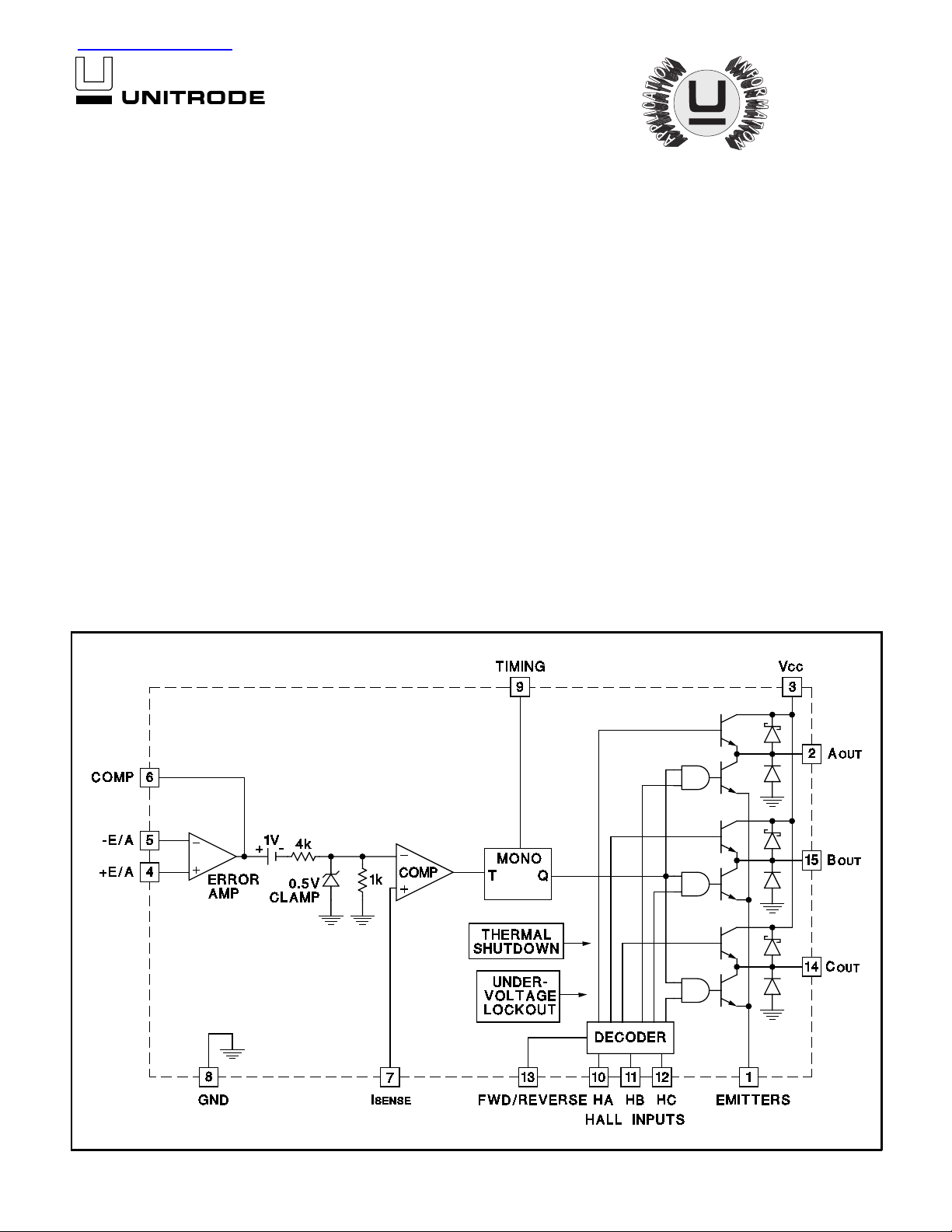
BLOCK DIAGRAM
DESCRIPTION
The UC3620 is a br ushless DC motor driver capable of decoding and
driving al l 3 windings of a 3-phase br ushles s DC motor. In addition, an
on-board c urrent comp arator, oscillator, and high gain Op-Amp provide
all necessar y circuitr y for implementing a high performance, chopped
mode servo amplifier. Full protection, including thermal shutdown,
pulse-by-pulse current limiting, and under-voltage lockout aid in the
simple implementation of reliable designs. Both conducted and radiated
EMI have been grea tly redu ced by limi ting the output dv/dt to 150V /µs
for any load condition.
The UC1620SP is characterized for operation over the full military temperature range of -55°C to +125°C, while the UC3620SP is characterized for 0°C to +70°C.
3/97
1
Page 2

UC1620
UC3620
ABSOLUTE MAXIMUM RATINGS
(Note 1)
Supply Voltage, VCC. . . . . . . . . . . . . . . . . . . . . . . . . . . . . . . 40V
Output Current, Source or Sink
CONNECTION DIAGRAMS
SP Hermetic Power DIL
Non-Repetitive (t = 100µsec), lo . . . . . . . . . . . . . . . . . . . . 3A
Repetitive (80% on - 20% off; tON = 10ms) . . . . . . . . . . 2.5A
DC Operation. . . . . . . . . . . . . . . . . . . . . . . . . . . . . . . . . . . 2A
Analog Inputs . . . . . . . . . . . . . . . . . . . . . . . . . . . . . -0.3 to +Vcc
Logic Inputs . . . . . . . . . . . . . . . . . . . . . . . . . . . . . . -0.3 to +Vcc
Total Power Dissipation (at T
CASE
= 75° C)
for SP Package (Note 2). . . . . . . . . . . . . . . . . . . . . . . . . . 15W
Storage Temperature . . . . . . . . . . . . . . . . . . . . -65°C to +150°C
Operating Junction Temperature . . . . . . . . . . . -55°C to +150°C
Note 1: All voltages are with respect to g round. Currents are
positive into, negative out of the specified terminal.
Note 2: Consult Packaging Section of Databook for thermal
limitations and considerations of package.
ELECTRICAL CHARACTERISTICS:
Unless otherwise stated, these spec ifications apply for TA = 0°C to 70°C for 3620; T
= 55°C to +125°C for UC1620; VCC = 20V, RT = 20V, RT = 10k, C
-2.2nF. TA=T
T =
PARAMETER TEST CONDITIONS UC3620 UC1 620 UNIT
MIN TYP MAX MIN TYP MAX
Error Amplifier Section
Input Offset Voltage 1.5 10 1.5 10 mV
Input Bias Current -.25 -2.0 -.25 -2.0 µA
Input Offset Current 15 250 15 250 nA
Common Mode Range Vcc = 8V to 40V 0 V
Open Loop Gain ∆V
Unity Gain Bandwidth T
Output Sink Current V
Output Source Current V
= 1V to 4V 80 100 75 100 dB
COMP
= 25°C, Note 2 0.8 0.8 MHz
J
= 1V 2 2 mA
COMP
= 4V 8 8 mA
COMP
-2 0 VIN-2 V
IN
Current Sense Section
Input Bias Current -2.0 -5 -2.0 -5 µA
Internal Clamp .425 0.5 .575 .405 0.5 .595 V
Divider Gain .180 0.2 .220 .170 0.2 .230 V/V
Internal Offset Voltage .8 1.0 1.2 .75 1.0 1.25 V
Timing Section
Output Off Tim e 18 20 22 17 20 23 µs
Upper Mono Threshold 5.0 5.0 V
Lower Mono Threshold 2.0 2.0 V
Decoder Section
High-Level Input Voltage 2.2 2.5 V
Low-Level Inpu t Vol ta ge 0.8 0.8 V
High-Level Input Current 10 10 µA
Low-Level Input Curre nt -10 -10 µA
Output Section
Output Leakage Curre nt V
VF1 Schottky Diode I
VF1 Substrat e Diode I
Total Output Voltage Drop I
= 40V 500 1500 µ A
CC
= 2A 1.5 2.0 1.5 2.0 V
O
= 2A 2.2 3.0 2.2 3.0 V
O
= 2A, Note 3 3.0 3.6 3.0 3.6 V
O
A
J.
2
Page 3
UC1620
UC3620
ELECTRICAL CHARACTERISTICS:
PARAMETER TEST CONDITIONS UC3620 UC1 620 UNIT
Output Section (cont.)
Output Rise Time R
Output Fall Time R
Under Voltage Lock ou t
Startup Threshold 8.0 8.0 V
Threshold Hysteresis 0.5 0.5 V
Thermal Shutdown
Junction Temperature Note 2 150 180 150 180 °C
Total Standby Current
Supply Current 32 55 32 55 mA
Note 2: These paramete rs , al th ou gh gu aranteed over the recommend ed op erating conditi on s , ar e no t 10 0% tes te d in prod uc ti on .
Note 3: The total voltage drop is defined as the sum of both top and bottom side driver.
TABLE 1
STEP FWD/
REV
1 1 101 H L O
2 1 100 H O L
3 1 110 O H L
4 1 010 L H O
5 1 011 L O H
6 1 001 O L H
1 0 101 L H O
2 0 100 L O H
3 0 110 O L H
4 0 010 H L O
5 0 011 H O L
6 0 001 O H L
H = HIGH OUTPUT
L = LOW OUTPUT
O = OPEN OUTPUT
Ha Hb Hc A
OUT
Unless otherwise stated, these spec ifications apply for T
= 55°C to +125°C for UC1620; VCC = 20V, RT = 20V, RT = 10k, C
MIN TYP MAX MIN TYP MAX
= 44Ω 150 150 ns
L
= 44Ω 150 150 ns
L
Hall lines require pull-up resistors.
B
OUT
C
OUT
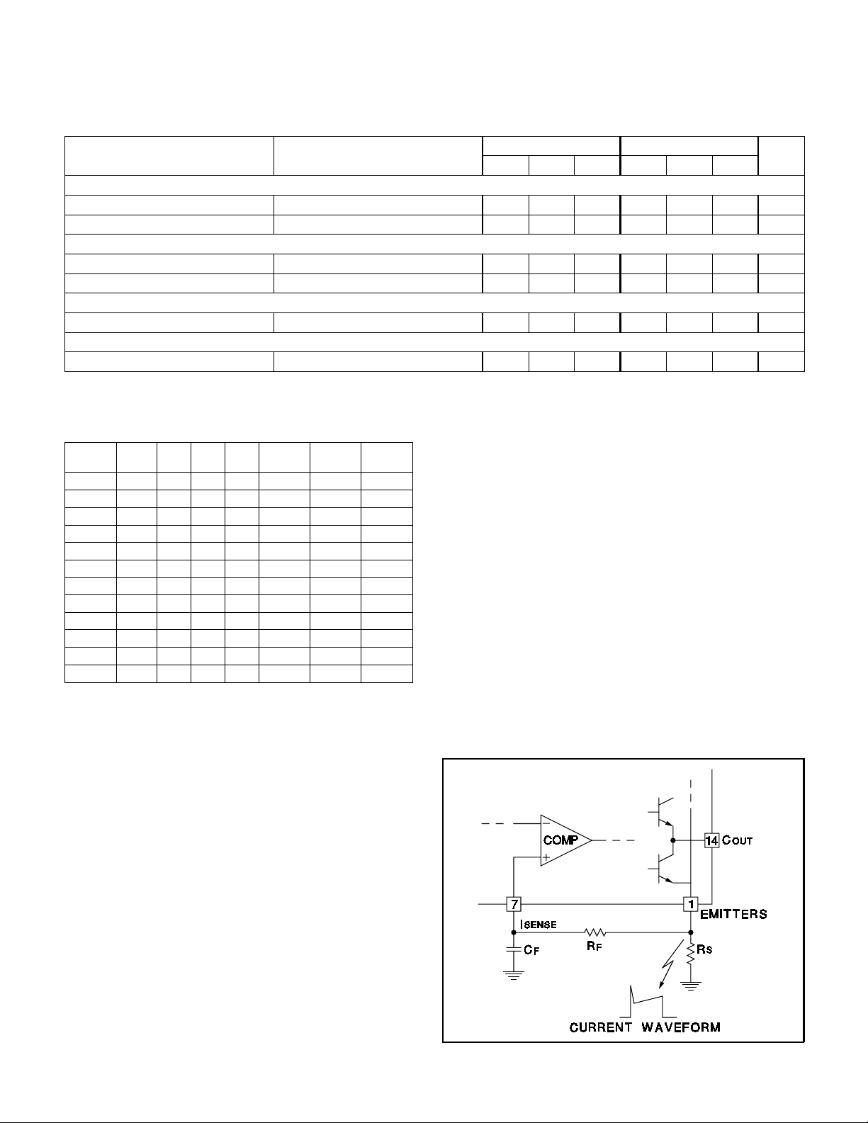
CURRENT SENSING
Referring to Figure 1, emitter current is sensed across R
and fed back through a low pass filter to the current
sense pin 7. This filter is required to eliminate false triggering of the monostable due to leading edge current
spikes. Actual filter values, although somewhat dependent on external loads, will generally be in the 1kΩ and
1000pF range.
TIMING
An R-C time constant on pin 9 is used by the monostable
to generate a fixed off time at the outputs according to the
formula:
T
OFF
=
As the peak current in the emitters approaches the value
at the minus (-) input of the on-board comparator, the
= 0°C to 70°C for 3620; T
A
T =
.916RTC
T
-2.2nF. TA=T
monostable is tr i gg er e d, c au s in g t he outputs to be tur ned
A
J.
S
CIRCUIT DESCRIPTION
The UC3620 is designed for implementation of a complete 3-∅ brushless DC servo drive using a minimum
number of external components. Below is a functional description of each major circuit feature.
DECODER
Table 1 shows the dec oding sc heme used in the UC3620
to decode and drive each of three high current totem pole
output sta ge s. A forward/reverse signal, pin 13, is used to
provide direc tion. At any point in time, one driver is sourcing, one dr iver is sin king, an d the rem aining driver is off
or tri-s tated. Pulse width modulation is acc omplished by
turning the sink driver off during the monostable reset
time, producing a fixed off-time chop mode. Controlled
output rise and fall times help reduce electrical switching
noise while maintaining re latively small switching loss es.
Figure 1.
3
Current Sense Filter
Page 4

CIRCUIT DESCRIPTION (cont.)
off. On time is det er m ined by the amount of time required
for motor current to increase to the value required to retrip the mono stable. A timing sequence of these events is
shown in Figure 2.
UC1620
UC3620
tive (-) input will limit peak current to a maximum value. A
fixed 0.5V internal clamp has been included on the
UC3620, and any current spike in the output which generates a sensed voltage greater than 0.5V will immediately shut down the outputs. Actual peak current values
may be programmed by selecting the appropriate value of
R
according to the formula:
S
Figure 2.
Chopped Mode Timi ng D iag ram
CURRENT LIMIT
Since peak current is being controlled at all times by the
internal comparator, a simple voltage clamp at its negative (-) input will limit peak current to a maximum value. A
fixed 0.5V internal clamp has been included on the
UC3620, and any current spike in the output which generates a sensed voltage greater than 0.5V will immediately
shut down the outputs. Actual peak current values may be
programmed by selecting the appropriate value of R
S
ac-
cording to the formula:
R
=
S
0.5
I
CURRENTLIMIT
Since peak current is being controlled at all times by the
internal comparator, a simple voltage clamp at its nega-
R
=
S
0.5
I
CURRENTLIMIT
ERROR AMPLIFIER LIMIT
A high perfor mance, on-board e rror amplifier is included
to facilitate implementing closed loop motor control. Error
voltage generati on and loop compe nsation are easily accomplished by appropriately configuring the gain and
feedback of this amplifier . To provide a larger dynamic signal range at the output of the er ror amplifier, a divide by 5
resistor net work is used to reduce the error signal level
before applying to the internal comparator. In addition, a
one volt offset has been introduced at the output of the
error amplifier to guarantee control down to zero current
in the output stages. Since this offset is divided by the
open loop gain of the feedback loop, it has virtually no effect on closed loop performance.
PROTECTION FUNCTIONS
Protective functions including under-voltage lockout, peak
current limiting, and thermal shutdown, provide an extremely rugged device capable of surviving under many
types of fault conditions. Under-voltage lockout guarantees the out puts will be off or tri- slated until V
is suffi-
CC
cient for proper operation of the chip. Current limiting
limits the peak current for a stalled or shorted motor,
whereas thermal shutdown will tr i-state the outputs if a
temperature above 150°C is reached.
4
Page 5

TYPICAL APPLICATIONS
UC1620
UC3620
*Both VCC PWR and VCC LOGIC pins must be connected together when using the SP package.
3-∅ Brushless DC Open Loop Motor Drive
*Both VCC PWR and VCC LOGIC pins must be connected together when using the SP package.
3-∅ Brushless DC Open Loop Motor with Current Limit at 2A.
5
Page 6

UC1620
UC3620
*Both VCC PWR and VCC LOGIC pins must be connected together when using the SP package.
Closed Loop Speed Control Servo
UNITRODE CORPORATION
7 CONTINENTAL BLVD. • MERRIMACK, NH 03054
TEL. (603) 424-2410 • FAX (603) 424-3460
6
Page 7

IMPORTANT NOTICE
T exas Instruments and its subsidiaries (TI) reserve the right to make changes to their products or to discontinue
any product or service without notice, and advise customers to obtain the latest version of relevant information
to verify, before placing orders, that information being relied on is current and complete. All products are sold
subject to the terms and conditions of sale supplied at the time of order acknowledgement, including those
pertaining to warranty, patent infringement, and limitation of liability.
TI warrants performance of its semiconductor products to the specifications applicable at the time of sale in
accordance with TI’s standard warranty. Testing and other quality control techniques are utilized to the extent
TI deems necessary to support this warranty . Specific testing of all parameters of each device is not necessarily
performed, except those mandated by government requirements.
CERTAIN APPLICATIONS USING SEMICONDUCTOR PRODUCTS MAY INVOLVE POTENTIAL RISKS OF
DEATH, PERSONAL INJURY, OR SEVERE PROPERTY OR ENVIRONMENTAL DAMAGE (“CRITICAL
APPLICATIONS”). TI SEMICONDUCTOR PRODUCTS ARE NOT DESIGNED, AUTHORIZED, OR
WARRANTED TO BE SUITABLE FOR USE IN LIFE-SUPPORT DEVICES OR SYSTEMS OR OTHER
CRITICAL APPLICA TIONS. INCLUSION OF TI PRODUCTS IN SUCH APPLICATIONS IS UNDERST OOD TO
BE FULLY AT THE CUSTOMER’S RISK.
In order to minimize risks associated with the customer’s applications, adequate design and operating
safeguards must be provided by the customer to minimize inherent or procedural hazards.
TI assumes no liability for applications assistance or customer product design. TI does not warrant or represent
that any license, either express or implied, is granted under any patent right, copyright, mask work right, or other
intellectual property right of TI covering or relating to any combination, machine, or process in which such
semiconductor products or services might be or are used. TI’s publication of information regarding any third
party’s products or services does not constitute TI’s approval, warranty or endorsement thereof.
Copyright 1999, Texas Instruments Incorporated
 Loading...