

Page 1
查询UC1543供应商
Power Supply Supervisory Circuit
DESCRIPTIONFEATURES
•
Includes Over-voltage,
Under-voltage, And Current
Sensing Circuits
•
Internal 1% Accurate
Reference
•
Programmable Time Delays
•
SCR “Crowbar” Drive Of
300mA
•
Remote Activation Capability
•
Optional Over-voltage Latch
•
Uncommitted Comparator
Inputs For Low Voltage
Sensing (UC1544 Series
Only)
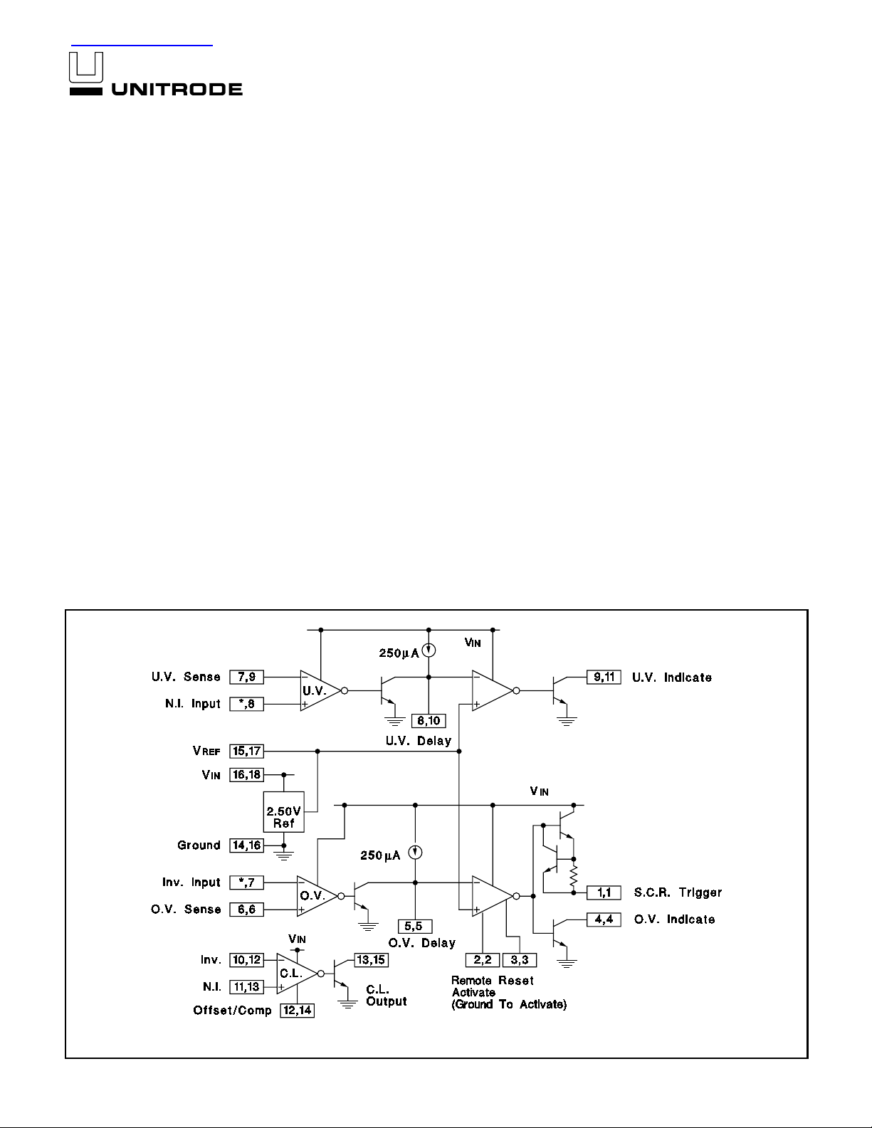
The monolithic integrated circuits contain all the functions necessar y to monitor
and control the output of a sophisticated power supply sy stem. Over-voltage (O.V.)
sensing with provision to t rigger an exter nal SCR “crowbar” shutdown; an undervoltage (U.V.) circuit which can be us ed to monitor either the output or to sample
the input line voltage; and a third op amp/comparator usable for current sensing
(C.L.) are all inclu ded in this IC, together with an independent, accurate reference
generator.
Both over- and under- voltage sensing circuits can be externally programmed for
minimum time dura tion of fault before tri ggeri ng. All functions contain open collector outputs wh ich can be used independently or wire-or’ed together, and although
the SCR trigger is directly connected only to the over-voltage sensing circuit, it
may be optionall y ac t ivate d by any of the other outputs, or fr om an external signal.
The O.V. circuit also includes an optional latch and external reset capability.
The UC1544/254 4/3544 devices have the ad ded versatility of completely uncommitted inputs to the voltage sensing c omparators so that levels less than 2.5V may
be monitored by dividing down the internal reference voltage. The current sense
circuit may be us ed wi th exter nal c ompen sation as a linear amplifier or as a highgain comparator. Although nominally s et for zero input offset, a fixed threshold may
be added with an external resistor. Instead of current limiting, this circuit may also
be used as an additional voltage monitor.
UC1543 UC1544
UC2543 UC2544
UC3543 UC3544
BLOCK DIAGRAM
The reference generat or circuit is internall y trimmed to el iminate the need for external potentiometers and the entire circuit may be powered directly from either the
output being monitored or from a separate bias voltage.
Note: For each terminal, firs t n um be r refers to 1543 series, se co nd to 15 44 series.
* On 1543 series, this function is internally connected to V
4/97
REF.
Page 2
ABSOLUTE MAXIMUM RATINGS
Input Supply Voltage, VIN. . . . . . . . . . . . . . . . . . . . . . . . . . . . . . . . . . . . . . 40V
Sense Inputs, Voltage Range. . . . . . . . . . . . . . . . . . . . . . . . . . . . . . . . 0 to V
SCR Trigger Current (Note 1) . . . . . . . . . . . . . . . . . . . . . . . . . . . . . . -600mA
Indicator Output Voltage. . . . . . . . . . . . . . . . . . . . . . . . . . . . . . . . . . . . . . . 40V
Indicator Output Sink Current. . . . . . . . . . . . . . . . . . . . . . . . . . . . . . . . . 50mA
Power Dissipation (Package Limitation). . . . . . . . . . . . . . . . . . . . . . . 1000mW
Operating Temp era ture Range
UC1543, UC1544 . . . . . . . . . . . . . . . . . . . . . . . . . . . . . . . . -55°C to +125°C
UC2543, UC2544 . . . . . . . . . . . . . . . . . . . . . . . . . . . . . . . . . -25°C to +85°C
UC3543, UC3544 . . . . . . . . . . . . . . . . . . . . . . . . . . . . . . . . . . 0°C to +70°C
Storage Temperature Range . . . . . . . . . . . . . . . . . . . . . . . . . -65°C to +150°C
IN
Note 1: At higher input voltages, a diss ipation limiti ng resistor, RG, is required.
Note 2: Currents are positive-into, negative-out of the specified terminal. Consult Packaging section of Databook for thermal limitations and considerations
of package.
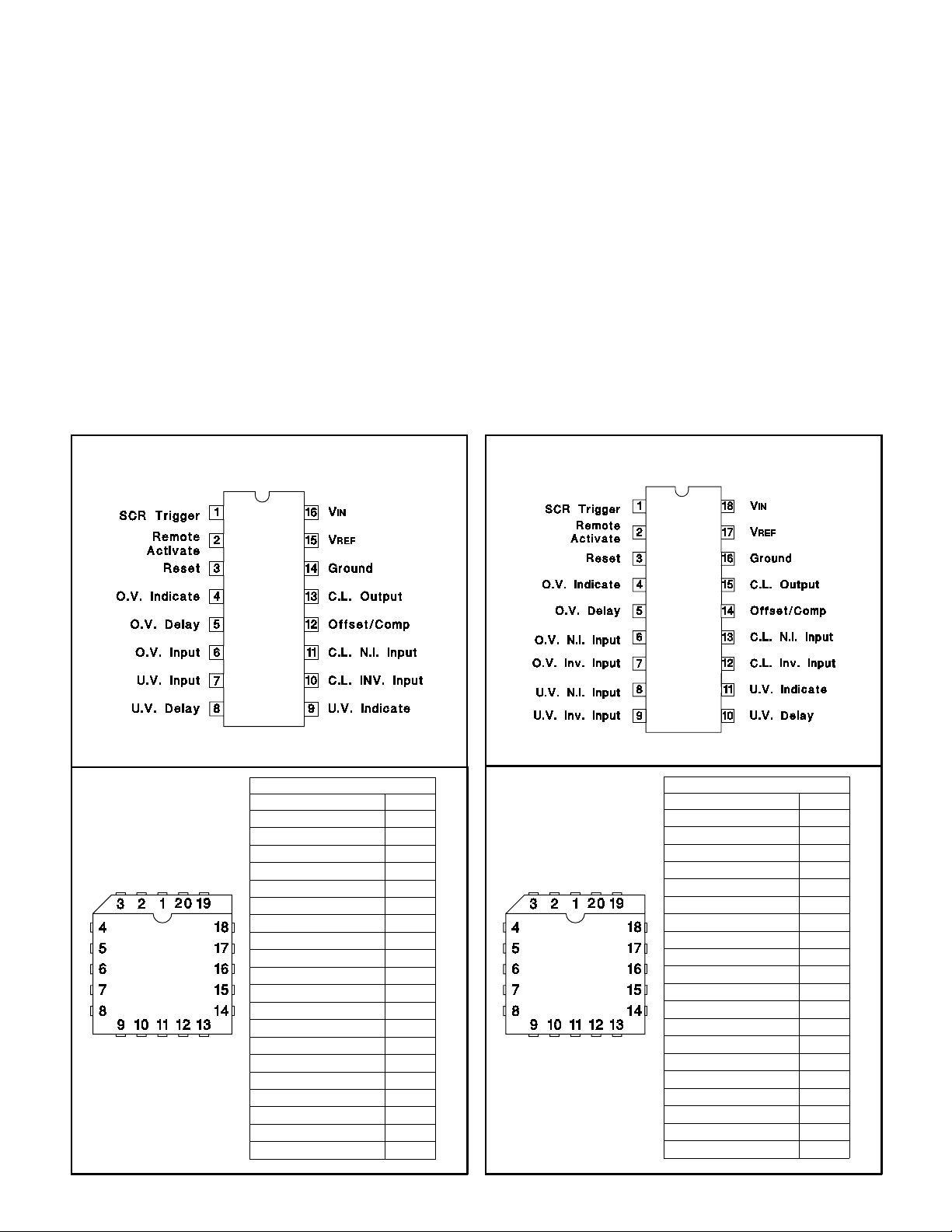
CONNECTION DIAGRAMS
UC1543 UC1544
UC2543 UC2544
UC3543 UC3544
DIL-16, SOIC-16 (TOP VIEW)
J or N, DW Package
PLCC-20, LCC-20
PACKAGE PIN FUNCTION
(TOP VIEW)
Q or L Package
N/C 1
SCR Trigger 2
Remote Activate 3
Reset 4
O.V. Indicate 5
N/C 6
O.V. Delay 7
O.V. Input 8
N/C 9
N/C 10
U.V. Input 1 1
U.V. Delay 12
U.V. Indicate 13
C.L. INV. Input 14
C.L. N.I. Input 15
Offset/Comp 16
C.L. Output 17
Ground 18
V
V
FUNCTION PIN
REF
IN
UC 1543
UC 2543
UC 3543
19
20
DIL-18, SOIC-18 (T OP VIEW)
J or N, DW Package
PLCC-20, LCC-20
PACKAGE PIN FUNCTION
(TOP VIEW)
Q or L Package
N/C 1
SCR Trigger 2
Remote Activate 3
Reset 4
O.V. Indicate 5
N/C 6
O.V. Delay 7
O.V. N.I. Input 8
O.V. INV. Input 9
U.V. N.I. Input 10
U.V. INV. Input 11
U.V. Delay 12
U.V. Indicate 13
C.L. INV. Input 14
C.L. N.I. Input 15
Offset/Comp 16
C.L. Output 17
Ground 18
V
V
FUNCTION PIN
REF
IN
UC 1544
UC 2544
UC 3544
19
20
2
Page 3
UC1543 UC1544
UC2543 UC2544
UC3543 UC3544
ELECTRICAL CHARACTERISTICS:
UC1543 and UC1 544; -25°C to +85°C for the UC2543 and UC2544; and 0°C to +70°C for the UC3543 and UC3544. Electrical
tests are performed with VIN = 10V and 2kΩ pull-up resistors on all indicator outputs. All electrical specifications for the UC1544,
UC2544, and UC3544 devices are tested with the inve rting over-voltage input and th e non-inverting under-voltage input externally
connected to the 2.5V reference. TA = T
PARAMETER TEST CONDITIONS
Input Voltage R ange T
Supply Current V
Reference Section
Output Voltage T
Output Voltage Over Temperature Range 2.45 2.55 2.40 2.60 V
Line Regulation V
Load Regulation I
Short Circuit Current V
Temperature Stability 50 50 ppm
SCR Trigger Section
Peak Output Current VIN = 5V, RG = 0, VO = 0 -100 -300 -600 -100 -300 -600 mA
Peak Output Voltage V
Output Off Voltage V
Remote Activate Current R/A Pin = Gnd -0.4 -0.8 -0.4 -0.8 mA
Remote Activate Voltage R/A Pin Open 2 6 2 6 V
Reset Current Reset = Gnd, R/A = Gnd -0.4 -0.8 -0.4 -0.8 mA
Reset Voltage Reset open, R/A = Gnd 2 6 2 6 V
Output Current Rise Time R
Prop. Delay from R/A R
Prop. Delay from O/V input R
Comparator Section
Input Threshold (Inp ut
voltage rising on O.V. and
falling on U.V.)
Input Hysteresis 25 25 mV
Input Bias Current Sense Input = 0V -0.3 -1.0 -0.3 -1.0
Delay Satura tion 0.2 0.5 0.2 0.5 V
Delay High Level 6 7 6 7 V
Delay Charging Current V
Indicate Saturation I
Indicate Leakage V
Propagation Delay Input Over Drive = 200mV, T
Current Limit Section
Input Voltage R ange 0 V
Input Bias Current Offset Pin Open, V
Input Offset Voltage Offset Pin Open, V
CMRR 0 ≤ VCM ≤ 12V, V
AVOL Offset Pin Open, V
Output Saturation I
Output Leakag e V
Small Signal Bandwidth A
Propagation Delay V
= 25°C to T
J
T
to T
MIN
= 40V, Output Open, TJ = 25°C 7 10 7 10 mA
IN
≤ TJ ≤ T
T
MIN
= 25°C 2.48 2.50 2.52 2.45 2.50 2.55 V
J
= 5 to 30V 1 5 1 5 mV
IN
= 0 to 10mA 1 10 1 10 mV
REF
= 0 -10 -20 -40 -12 -20 -40 mA
REF
= 15V, IO = -100mA 12 13 12 13 V
IN
= 40V 0 0.1 0 0.1 V
IN
= 50Ω, TJ = 25°C, CD = 0 400 400 mA/µs
L
= 50Ω, TJ = 25°C, CD = 0 300 300 ns
L
= 50Ω, TJ = 25°C, CD = 0 500 500 ns
L
= 25°C 2.45 2.50 2.55 2.40 2.50 2.60 V
T
J
Over Temperature Range 2.40 2.60 2.35 2.65 V
= 0 -200 -250 -300 -200 -250 -300 µA
O
= 10mA 0.2 0.5 0.2 0.5 V
L
= 40V .01 1.0 .01 1.0 µA
IND
Input Over Drive = 200mV, T
10kΩ from Offset Pin to Gnd 80 100 120 80 100 120 mV
RL = 10k to 15kΩ, ∆V
= 10mA 0.2 0.5 0.2 0.5 V
L
= 40V .01 1.0 .01 1.0 µA
IND
= 0dB, TJ = 25°C 5 5 MHz
V
OVERDRIVE
Unless otherwise stated, these specif ic ations apply for TA = -55°C to +125°C for the
J.
UC1543/UC1544
UC3543/UC3544 UNITS
UC2543/UC2544
MIN TYP MAX MIN TYP MAX
4.5 40 4.5 40 V
4.7 40 4.7 40 V
15 15 mA
-3V 0 V
IN
3V V
IN
-
72 80 72 80 dB
MAX
MAX
MAX
= 25°C, CD = 0 400 400 ns
J
= 25°C, CD = 1µF10 10 ms
J
= 0 -0.3 -1.0 -0.3 -1.0
CM
= 0 0 10 0 10 mV
CM
= 15V 6070 6070 dB
IN
= 0V,
CM
= 1 to 6V
OUT
= 100mV, TJ = 25°C 200 200 ns
µ
A
µ
A
/°C
3
Page 4
UC1543 UC1544
UC2543 UC2544
UC3543 UC3544
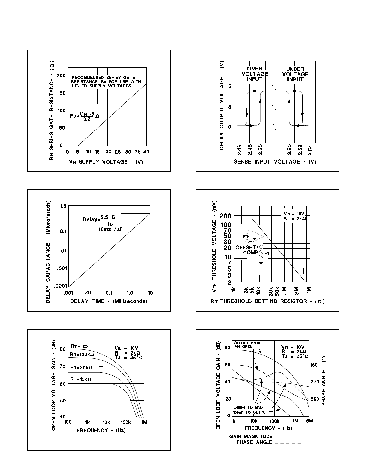
SCR T rigger P o wer Limiting
Activation Delay vs Capacitor Value
Comparator Input Hysteresis
Current Limit Input Threshold
Current Limit Amplifier Gain
Note: RT is connected from Offset Pin to Gnd. Values of
R
below 5.0k may cause Amplifier Cutoff at -55°C.
T
Current Limit Amplifier Frequency Response
4
Page 5

UC1543 UC1544
UC2543 UC2544
UC3543 UC3544
APPLICATIONS
(Pin numbers given for UC1543 series devices)
Typical Application
Sensing Multiple Supply Voltages
The values for the external components are determined
as follows:
Current limit input threshold, VTH =
is determ ined by the current loop dynamics
C
S
Peak current to load, I
Short Circuit Current, ISC =
Low outpu t voltage limi t, VO (Low) =
High output voltage limit, VO (High) =
Voltage sens ing delay, tD = 10,000Cd
SCR trigger power limiting resistor, R
1000
R
1
V
V
TH
≅
P
+
R
R
SC
V
TH
R
SC
O
SC
2.5
2.5
G
R
>
2
(R
R
2
+ R
3
+ R5 + R
4
R5 + R
(R
+ R5 + R
4
R
VIN − 5
0.2
)
6
6
)
6
6
UNITRODE CORPORATION
7 CONTINENTAL BLVD. • MERRIMACK, NH 03054
TEL. (603) 424-2410 • FAX 603-424-3460
Overcurrent ShutdownInput Line Monitor
5
Page 6

IMPORTANT NOTICE
T exas Instruments and its subsidiaries (TI) reserve the right to make changes to their products or to discontinue
any product or service without notice, and advise customers to obtain the latest version of relevant information
to verify, before placing orders, that information being relied on is current and complete. All products are sold
subject to the terms and conditions of sale supplied at the time of order acknowledgement, including those
pertaining to warranty, patent infringement, and limitation of liability.
TI warrants performance of its semiconductor products to the specifications applicable at the time of sale in
accordance with TI’s standard warranty. Testing and other quality control techniques are utilized to the extent
TI deems necessary to support this warranty . Specific testing of all parameters of each device is not necessarily
performed, except those mandated by government requirements.
CERTAIN APPLICA TIONS USING SEMICONDUCT OR PRODUCTS MAY INVOLVE POTENTIAL RISKS OF
DEATH, PERSONAL INJURY, OR SEVERE PROPERTY OR ENVIRONMENTAL DAMAGE (“CRITICAL
APPLICATIONS”). TI SEMICONDUCTOR PRODUCTS ARE NOT DESIGNED, AUTHORIZED, OR
WARRANTED TO BE SUITABLE FOR USE IN LIFE-SUPPORT DEVICES OR SYSTEMS OR OTHER
CRITICAL APPLICA TIONS. INCLUSION OF TI PRODUCTS IN SUCH APPLICATIONS IS UNDERST OOD TO
BE FULLY AT THE CUSTOMER’S RISK.
In order to minimize risks associated with the customer’s applications, adequate design and operating
safeguards must be provided by the customer to minimize inherent or procedural hazards.
TI assumes no liability for applications assistance or customer product design. TI does not warrant or represent
that any license, either express or implied, is granted under any patent right, copyright, mask work right, or other
intellectual property right of TI covering or relating to any combination, machine, or process in which such
semiconductor products or services might be or are used. TI’s publication of information regarding any third
party’s products or services does not constitute TI’s approval, warranty or endorsement thereof.
Copyright 1999, Texas Instruments Incorporated
 Loading...