

Page 1
查询5962-8764502EA供应商
Advanced Regulating Pulse Width Modulators
UC1524A
UC2524A
UC3524A
FEATURES
Fully Interchangeable with
•
Standard UC1524 Family
Precision Reference Internally
•
Trimmed to±1%
High-Performance Current Limit
•
Function
Under-Voltage Lockout with
•
Hysteretic Turn-on
Start-Up Supply Current Less
•
Than 4mA
Output Current to 200mA
•
60V Output Capability
•
Wide Common-Mode Input
•
Range for both Error and
Current Limit Amplifiers
• PWM Latch Insures Single
Pulse per Period
• Double Pulse Suppression
Logic
• 200ns Shutdown through PWM
Latch
•
Guaranteed Frequency
Accuracy
•
Thermal Shutdown Protection
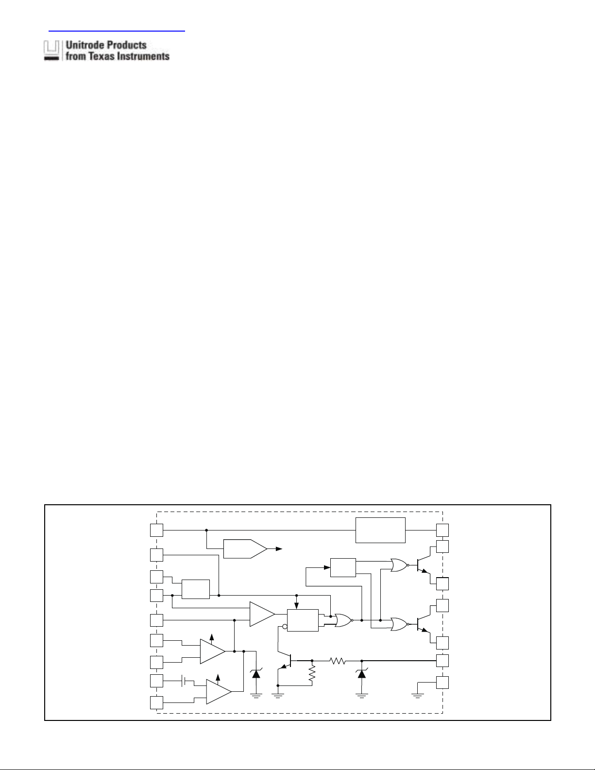
BLOCK DIAGRAM
DESCRIPTION
The UC1524A family of regulating PWM ICs has been designed to retain the
same highly versatile architecture of the industry standard UC1524 (SG1524)
while offering substantial improvements to many of its limitations. The UC1524A
is pin compatible with “non-A” models and in most existing applications can be
directly interchanged with no effect on power supply performance. Using the
UC1524A, however, frees the designer from many concerns which typically had
required additional circuitry to solve.
The UC1524A includes a precise 5V reference trimmed to±1% accuracy, elimi
nating the need for potentiometer adjustments; an error amplifier with an input
range which includes 5V, eliminating the need for a reference divider; a current
sense amplifier useful in either the ground or power supply output lines; and a
pair of 60V, 200mA uncommitted transistor switches which greatly enhance out
put versatility.
An additional feature of the UC1524A is an under-voltage lockout circuit which
disables all the internal circuitry, except the reference, until the input voltage has
risen to 8V. This holds standby current low until turn-on, greatly simplifying the
design of low power, off-line supplies. The turn-on circuit has approximately
600mV of hysteresis for jitter-free activation.
Other product enhancements included in the UC1524A’s design include a PWM
latch which insures freedom from multiple pulsing within a period, even in noisy
environments, logic to eliminate double pulsing on a single output, a 200ns external shutdown capability, and automatic thermal protection from excessive
chip temperature . The oscillator circuit of the UC1524A is usable bey ond 500kHz
and is now easier to synchronize with an external clock pulse.
The UC1524A is packaged in a hermetic 16-pin DIP and is rated for operation
from -55°C to +125°C. The UC2524A and 3524A are available in either ceramic
or plastic packages and are rated for operation from -40°C to +85°C and 0°C to
70°C, respectively. Surface mount devices are also available.
-
-
15
V
IN
3
OSC
6
R
T
7
C
T
COMP
INV. INPUT
N.I. INPUT
CL (+) SENSE
CL (–) SENSE
9
1
2
4
5
SLUS181A - NOVEMBER 1999
200mV
+
OSC
–
E/A
E/A
+
V
RAMP
IN
V
IN
+
C/L
–
U.V.
SENSE
CLOCK
COMP
+
–
6V
POWER TO
INTERNAL
CIRCUITRY
R
S
PWM
S
LATCH
10k
+5V
REFERENCE
REGULATOR
FLIP
FLOP
T
1k
5.5V
16
V
12
C
11
E
13
C
14
E
10
SHUTDOWN
GND
8
REF
A
A
B
B
UDG-99178
Page 2
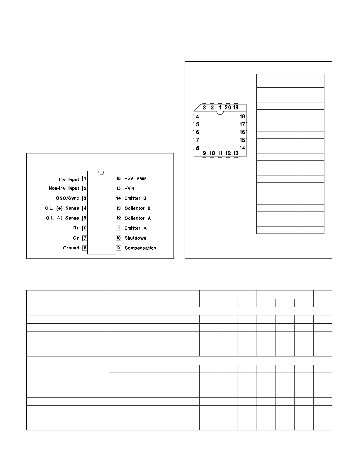
ABSOLUTE MAXIMUM RATINGS
Supply Voltage (VIN) . . . . . . . . . . . . . . . . . . . . . . . . . . . . . . 40V
Collector Supply Voltage (V
Output Current (each Output). . . . . . . . . . . . . . . . . . . . . 200mA
Maximum Forced Voltage (Pin 9, 10) . . . . . . . . . . . . . -3 to +5V
Maximum Forced Current (Pin 9, 10) . . . . . . . . . . . . . . . ±10mA
Reference Output Current . . . . . . . . . . . . . . . . . . . . . . . . 50mA
Oscillator Charging Current . . . . . . . . . . . . . . . . . . . . . . . . 5mA
Power Dissipation at T
Power Dissipation at T
Operating Temperature Range . . . . . . . . . . . . -55°C to +125°C
Storage Temperature Range. . . . . . . . . . . . . . -65°C to +150°C
Lead Temperature, (Soldering, 10 seconds) . . . . . . . . . +300°C
Note: Consult packaging section of Databook for thermal limita
tions and considerations of package.
DIL-16, SOIC-16 (TOP VIEW)
J or N Package, DW Package
C) . . . . . . . . . . . . . . . . . . . . . . . 60V
A = +25°C. . . . . . . . . . . . . . . . . 1000mW
C = +25°C . . . . . . . . . . . . . . . . 2000mW
CONNECTION DIAGRAMS
PLCC-20, LCC-20 (TOP VIEW)
Q or L Package
-
UC1524A
UC2524A
UC3524A
PACKAGE PIN FUNCTION
FUNCTION PIN
N/C 1
Inv. Input 2
Non-Inv. Input 3
OSC/SYNC 4
C.L. (+) sense 5
N/C 6
C.L. (-) sense 7
T 8
R
T 9
C
Ground 10
N/C 11
Compensation 12
Shutdown 13
Emitter A 14
Collector A 15
N/C 16
Collector B 17
Emitter B 18
IN 19
+V
REF 20
+5V V
ELECTRICAL CHARACTERISTICS:
Unless otherwise stated, these specifications apply for TA = -55°C to +125°C for the
UC1524A, -40° to +85°C for the UC2524A, and 0°C to + 70°C for the UC3524A; V
= VC = 20V, TA =TJ.
UC1524A / UC2524A UC3524A UNITS
PARAMETER TEST CONDITIONS
MIN TYP MAX MIN TYP MAX
Turn-on Characteristics
Input Voltage Operating Range after Turn-on 8 40 8 40 V
Turn-on Threshold 6.5 7.5 8.5 6.5 7.5 8.5 V
Turn-on Current V
Operating Current V
IN = 6V 2.5 4 2.5 4 mA
IN = 8 to 40V 5 10 5 10 mA
Turn-on Hysteresis* 0.5 0.5 V
Reference Section
Output Voltage T
J = 25°C 4.95 5.00 5.05 4.90 5.00 5.10 V
Over Operating Range 4.9 5.1 4.85 5.15 V
Line Regulation V
Load Regulation I
IN = 10 to 40V 10 20 10 30 mV
L = 0 to 20 mA 20 25 20 35 mV
Temperature Stability* Over Operating Range* 20 25 20 35 mV
Short Circuit Current V
REF = 0, 25°C
Output Noise Voltage* 10Hz≤f≤10kHz, T
Long Term Stability* T
J =125°C, 1000 Hrs. 20 50 20 50 mV
TJ≤125°C 80 100 80 100 mA
≤
J =25°C 40 40
* These parameters are ensured by design but not 100% tested in production.
Vrms
µ
IN
2
Page 3
UC1524A
UC2524A
UC3524A
ELECTRICAL CHARACTERISTICS:
Unless otherwise stated, these specifications apply for TA = -55°C to +125°C for the
UC1524A, -40° to +85°C for the UC2524A, and 0°C to + 70°C for the UC3524A; V
= VC = 20V, TA =TJ.
UC1524A / UC2524A UC3524A UNITS
PARAMETER TEST CONDITIONS
Oscillator Section (Unless otherwise specified, R
Initial Accuracy T
J = 25°C 414345394347kHz
T = 2700
, CT = 0.01 mfd)
Ω
MIN TYP MAX MIN TYP MAX
Over Operating Range 40.2 45.9 38.2 47.9 kHz
Temperature Stability* Over Operating Temperature Range 1 2 1 2 %
Minimum Frequency R
Maximum Frequency R
T = 150k
T = 2.0k
, CT = 0.1mfd 140 120 Hz
Ω
, CT = 470pF 500 500 kHz
Ω
Output Amplitude* 3 3.5 3 3.5 V
Output Pulse Width* 0.29 0.5 1.0 0.3 0.5 1.0
Ramp Peak 3.3 3.5 3.7 3.3 3.5 3.7 V
Ramp Valley T
J = 25°C 0.7 0.8 0.9 0.7 0.8 0.9 V
Ramp Valley T.C. -1.0 -1.0 mV/°C
Error Amplifier Section (Unless otherwise specified, V
CM = 2.5V)
Input Offset Voltage 0.5 5 2 10 mV
Input Bias Current 1 5 1 10
Input Offset Current .05 1 0.5 1
Common Mode Rejection Ratio V
Power Supply Rejection Ratio V
CM = 1.5 to 5.5V 70 80 70 80 dB
IN = 10 to 40V 70 80 70 80 dB
Output Swing (Note 1) 5.0 0.5 5.0 0.5 V
Open Loop Voltage Gain
Gain-Bandwidth* T
DC Transconductance*§ T
P.W.M. Comparator (R
T = 2k
Ω
Minimum Duty Cycle V
Maximum Duty Cycle V
O= 1 to 4V, RL
V
∆
J =25°C, AV = 0dB 1 3 1 3 MHz
J = 25°C, 30k
, CT = 0.01mfd)
COMP = 0.5V 0 0 %
COMP = 3.8V 45 45 %
10M
≥
Ω≤
RL
Ω
≤1MΩ
72 80 64 80 dB
1.7 2.3 1.7 2.3 mS
Current Limit Amplifier (Unless otherwise specified, Pin 5 = 0V)
Input Offset Voltage T
J = 25°C, E/A Set for Maximum
190 200 210 180 200 220 mV
Output
Over Operating Temperature Range 180 220 170 230 mV
Input Bias Current -1 -10 -1 -10
Common Mode Rejection Ratio V
Power Supply Rejection Ratio V
(pin 5) = -0.3V to + 5.5V 50 60 50 60 dB
IN = 10 to 40V 50 60 50 60 dB
Output Swing (Note 1) Minimum Total Range 5.0 0.5 5.0 0.5 V
Open-Loop Voltage Gain
O = 1 to 4V, RL
V
∆
Delay Time* Pin 4 to Pin 9,∆V
10M
≥
Ω
IN = 300mV 300 300 ns
70 80 70 80 dB
Output Section (Each Output)
Collector Emitter Voltage I
Collector Leakage Current V
C = 100
CE = 50V .1 20 .1 20
A 6080 6080 V
µ
IN
s
µ
A
µ
A
µ
A
µ
A
µ
* These parameters are ensured by design but not 100% tested in production.
§ DC transconductance (g
M
) relates to DC open-loop voltage gain according to the following equation:AV=gMR
where RLis the resistance from pin 9 to the common mode voltage.
The minimum g
M
specification is used to calculate minimum AVwhen the error amplifier output is loaded.
Note 1: Min Limit applies to output high level, max limit applies to output low level.
3
L
Page 4

UC1524A
UC2524A
UC3524A
ELECTRICAL CHARACTERISTICS:
Unless otherwise stated, these specifications apply for TA = -55°C to +125°C for the
UC1524A, -40° to +85°C for the UC2524A, and 0°C to + 70°C for the UC3524A; V
= VC = 20V. TA =TJ.
UC1524A / UC2524A UC3524A UNITS
PARAMETER TEST CONDITIONS
MIN TYP MAX MIN TYP MAX
Output Section ( cont.) (Each Output)
Saturation Voltage I
Emitter Output Voltage I
Rise Time* T
Fall Time* T
Comparator Delay* T
Shutdown Delay* T
Shutdown Threshold T
C = 20mA
I
C = 200mA
E = 50mA 17 18 17 18 V
J=25°C, R = 2k
J = 25°C, R = 2k
J = 25°C, Pin 9 to output 300 300 ns
J = 25°C, Pin 10 to output 200 200 ns
J = 25°C, RC = 2k
Ω
Ω
Ω
0.6 .7 1.0 0.6 .7 1.0 V
.2
1
.4
2.2
.2
1
.4
2.2
120 400 120 400 ns
25 200 25 200 ns
S/D Threshold Over Temp. Over Operating Temperature Range 0.4 1.2 0.4 1.0 V
Thermal Shutdown* 165 165 °C
* These parameters are ensured by design but not 100% tested in production.
OPEN-LOOP CIRCUIT
IN
V
V
4
Page 5

UC1524A
UC2524A
UC3524A
Supply Current vs Voltage
Pulse Width Modulator
Transfer Function
Error Amplifier Voltage Gain
and Phase vs Frequency
Oscillator Frequency
vs Timing Components
Output Dead Time vs Timing Capacitor Value
Output Saturation Voltage
5
Page 6

UC1524A
UC2524A
UC3524A
Current Limit Amplifier Delay
Turn-Off Delay From Shutdown - Pin 10
Shutdown Delay From PWM Comparator - Pin 9
6
Page 7

PACKAGE OPTION ADDENDUM
www.ti.com
4-Mar-2005
PACKAGING INFORMATION
Orderable Device Status
(1)
Package
Type
Package
Drawing
Pins Package
Qty
Eco Plan
5962-8764502EA ACTIVE CDIP J 16 1 None A42 SNPB Level-NC-NC-NC
UC1524AJ ACTIVE CDIP J 16 1 None A42 SNPB Level-NC-NC-NC
UC1524AJ/80503 ACTIVE CDIP J 16 1 None A42 SNPB Level-NC-NC-NC
UC1524AJ883B ACTIVE CDIP J 16 1 None A42 SNPB Level-NC-NC-NC
UC1524AL ACTIVE LCCC FK 20 1 None POST-PLATE Level-NC-NC-NC
UC1524AL883B ACTIVE LCCC FK 20 1 None POST-PLATE Level-NC-NC-NC
UC2524ADW ACTIVE SOIC DW 16 40 None CU NIPDAU Level-2-220C-1 YEAR
UC2524ADWTR ACTIVE SOIC DW 16 2000 None CU NIPDAU Level-2-220C-1 YEAR
UC2524AJ ACTIVE CDIP J 16 1 None A42 SNPB Level-NC-NC-NC
UC2524AN ACTIVE PDIP N 16 25 None CU SNPB Level-NA-NA-NA
UC2524ANG4 ACTIVE PDIP N 16 1000 Green (RoHS &
no Sb/Br)
UC3524ADW ACTIVE SOIC DW 16 40 None CU NIPDAU Level-2-220C-1 YEAR
UC3524ADWTR ACTIVE SOIC DW 16 2000 None CU NIPDAU Level-2-220C-1 YEAR
UC3524AJ ACTIVE CDIP J 16 1 None A42 SNPB Level-NC-NC-NC
UC3524AN ACTIVE PDIP N 16 25 None CU SNPB Level-NA-NA-NA
(1)
The marketing status values are defined as follows:
ACTIVE: Product device recommended for new designs.
LIFEBUY: TI has announced that the device will be discontinued, and a lifetime-buy period is in effect.
NRND: Not recommended for new designs. Device is in production to support existing customers, but TI does not recommend using this part in
a new design.
PREVIEW: Device has been announced but is not in production. Samples may or may not be available.
OBSOLETE: TI has discontinued the production of the device.
(2)
Lead/Ball Finish MSL Peak Temp
CU NIPDAU Level-NA-NA-NA
(3)
(2)
Eco Plan - May not be currently available - please check http://www.ti.com/productcontent for the latest availability information and additional
product content details.
None: Not yet available Lead (Pb-Free).
Pb-Free (RoHS): TI's terms "Lead-Free" or "Pb-Free" mean semiconductor products that are compatible with the current RoHS requirements
for all 6 substances, including the requirement that lead not exceed 0.1% by weight in homogeneous materials. Where designed to be soldered
at high temperatures, TI Pb-Free products are suitable for use in specified lead-free processes.
Green (RoHS & no Sb/Br): TI defines "Green" to mean "Pb-Free" and in addition, uses package materials that do not contain halogens,
including bromine (Br) or antimony (Sb) above 0.1% of total product weight.
(3)
MSL, Peak Temp. -- The Moisture Sensitivity Level rating according to the JEDECindustry standard classifications, and peak solder
temperature.
Important Information and Disclaimer:The information provided on this page represents TI's knowledge and belief as of the date that it is
provided. TI bases its knowledge and belief on information provided by third parties, and makes no representation or warranty as to the
accuracy of such information. Efforts are underway to better integrate information from third parties. TI has taken and continues to take
reasonable steps to provide representative and accurate information but may not have conducted destructive testing or chemical analysis on
incoming materials and chemicals. TI and TI suppliers consider certain information to be proprietary, and thus CAS numbers and other limited
information may not be available for release.
In no event shall TI's liability arising out of such information exceed the total purchase price of the TI part(s) at issue in this document sold by TI
to Customer on an annual basis.
Addendum-Page 1
Page 8

IMPORTANT NOTICE
Texas Instruments Incorporated and its subsidiaries (TI) reserve the right to make corrections, modifications,
enhancements, improvements, and other changes to its products and services at any time and to discontinue
any product or service without notice. Customers should obtain the latest relevant information before placing
orders and should verify that such information is current and complete. All products are sold subject to TI’s terms
and conditions of sale supplied at the time of order acknowledgment.
TI warrants performance of its hardware products to the specifications applicable at the time of sale in
accordance with TI’s standard warranty. Testing and other quality control techniques are used to the extent TI
deems necessary to support this warranty . Except where mandated by government requirements, testing of all
parameters of each product is not necessarily performed.
TI assumes no liability for applications assistance or customer product design. Customers are responsible for
their products and applications using TI components. To minimize the risks associated with customer products
and applications, customers should provide adequate design and operating safeguards.
TI does not warrant or represent that any license, either express or implied, is granted under any TI patent right,
copyright, mask work right, or other TI intellectual property right relating to any combination, machine, or process
in which TI products or services are used. Information published by TI regarding third-party products or services
does not constitute a license from TI to use such products or services or a warranty or endorsement thereof.
Use of such information may require a license from a third party under the patents or other intellectual property
of the third party, or a license from TI under the patents or other intellectual property of TI.
Reproduction of information in TI data books or data sheets is permissible only if reproduction is without
alteration and is accompanied by all associated warranties, conditions, limitations, and notices. Reproduction
of this information with alteration is an unfair and deceptive business practice. TI is not responsible or liable for
such altered documentation.
Resale of TI products or services with statements different from or beyond the parameters stated by TI for that
product or service voids all express and any implied warranties for the associated TI product or service and
is an unfair and deceptive business practice. TI is not responsible or liable for any such statements.
Following are URLs where you can obtain information on other Texas Instruments products and application
solutions:
Products Applications
Amplifiers amplifier.ti.com Audio www.ti.com/audio
Data Converters dataconverter.ti.com Automotive www.ti.com/automotive
DSP dsp.ti.com Broadband www.ti.com/broadband
Interface interface.ti.com Digital Control www.ti.com/digitalcontrol
Logic logic.ti.com Military www.ti.com/military
Power Mgmt power.ti.com Optical Networking www.ti.com/opticalnetwork
Microcontrollers microcontroller.ti.com Security www.ti.com/security
Telephony www.ti.com/telephony
Video & Imaging www.ti.com/video
Wireless www.ti.com/wireless
Mailing Address: Texas Instruments
Post Office Box 655303 Dallas, Texas 75265
Copyright 2005, Texas Instruments Incorporated
 Loading...