

Page 1
DESCRIPTI ON
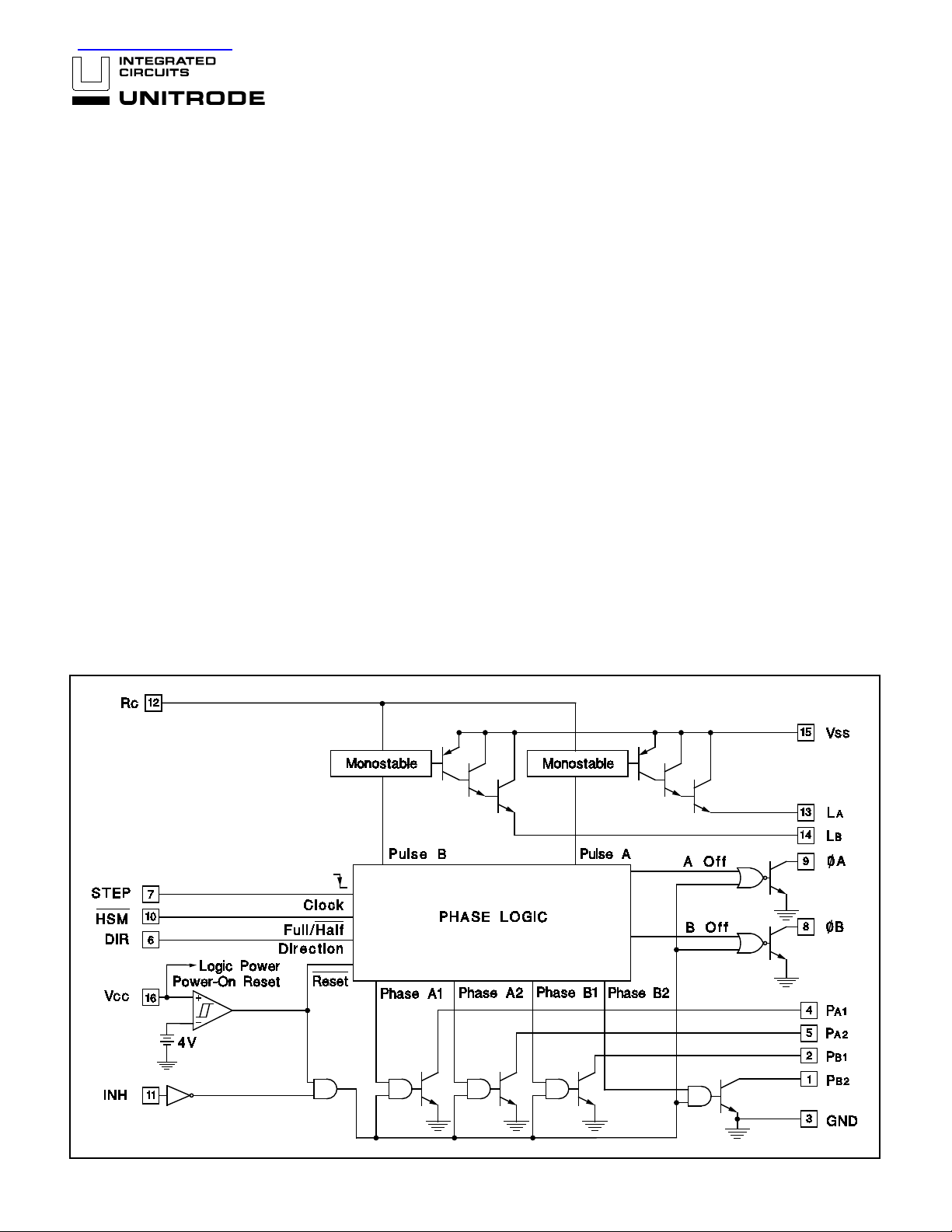
The UC3517 contains four NPN drivers that operate in two-phase
fashion for full-step and half-step motor control. The UC3517
also contains two emitter followers, two monostables, phase decoder logic, power-on reset, and low-voltage protection, making it
a versatile system for driving small stepper motors or for controlling large power devices.
The emitter followers and monostables in the UC3517 are configured to apply higher-voltage pulses to the motor at each step
command. This drive technique, called “Bilevel,” allows faster
stepping than common resistive current limiting, yet generates
less electrical noise than chopping techniques.
查询UC1517供应商
Stepper Motor Drive Circuit
FEATURES
• Complete Motor Driver and Encoder
• Continuous Drive Capability 350mA per Phase
• Contains all Required Logic for Full and Half
Stepping
• Bilevel Operation for Fast Step Rates
• Operates as a Voltage Doubler
• Useable as a Phase Generator and/or as a
Driver
• Power-On Reset Guarantees Saf e,
Predictable Power-Up
ABSOLUTE MAXI MUM RATING S
Second Level Supply , VSS . . . . . . . . . . . . . . . . . . . . . . . . . . 40V
Phase Outp u t Sup ply, V
Logic Supply, V
Logic Input Volt age . . . . . . . . . . . . . . . . . . . . . . . . . -.3V to +7V
Logic Input Cur ren t . . . . . . . . . . . . . . . . . . . . . . . . . . . . . ±10mA
Output Current , Each Phas e . . . . . . . . . . . . . . . . . . . . . . 500mA
Output Current , Emit ter Follower . . . . . . . . . . . . . . . . . . -500mA
Power Dissipation , (Note). . . . . . . . . . . . . . . . . . . . . . . . . . . . 1W
CC. . . . . . . . . . . . . . . . . . . . . . . . . . . . . . . . . . 7V
MM . . . . . . . . . . . . . . . . . . . . . . . . . 40 V
UC1517
UC3517
Power Dissipation , (Note) . . . . . . . . . . . . . . . . . . . . . . . . . . . 2W
Junction Te mp era ture . . . . . . . . . . . . . . . . . . . . . . . . . . . . 150°C
Ambient Temperatu re, UC151 7. . . . . . . . . . . . -55°C to +125°C
Ambient Temperature, UC3517 . . . . . . . . . . . . . . 0°C to +70°C
Storage Tem per at ure . . . . . . . . . . . . . . . . . . . -55°C to +150°C
Note: Consult Packag ing sect ion of Databook for therma l
limitations and cons iderations of package.
BLOCK DIAGRAM
8/94
Page 2
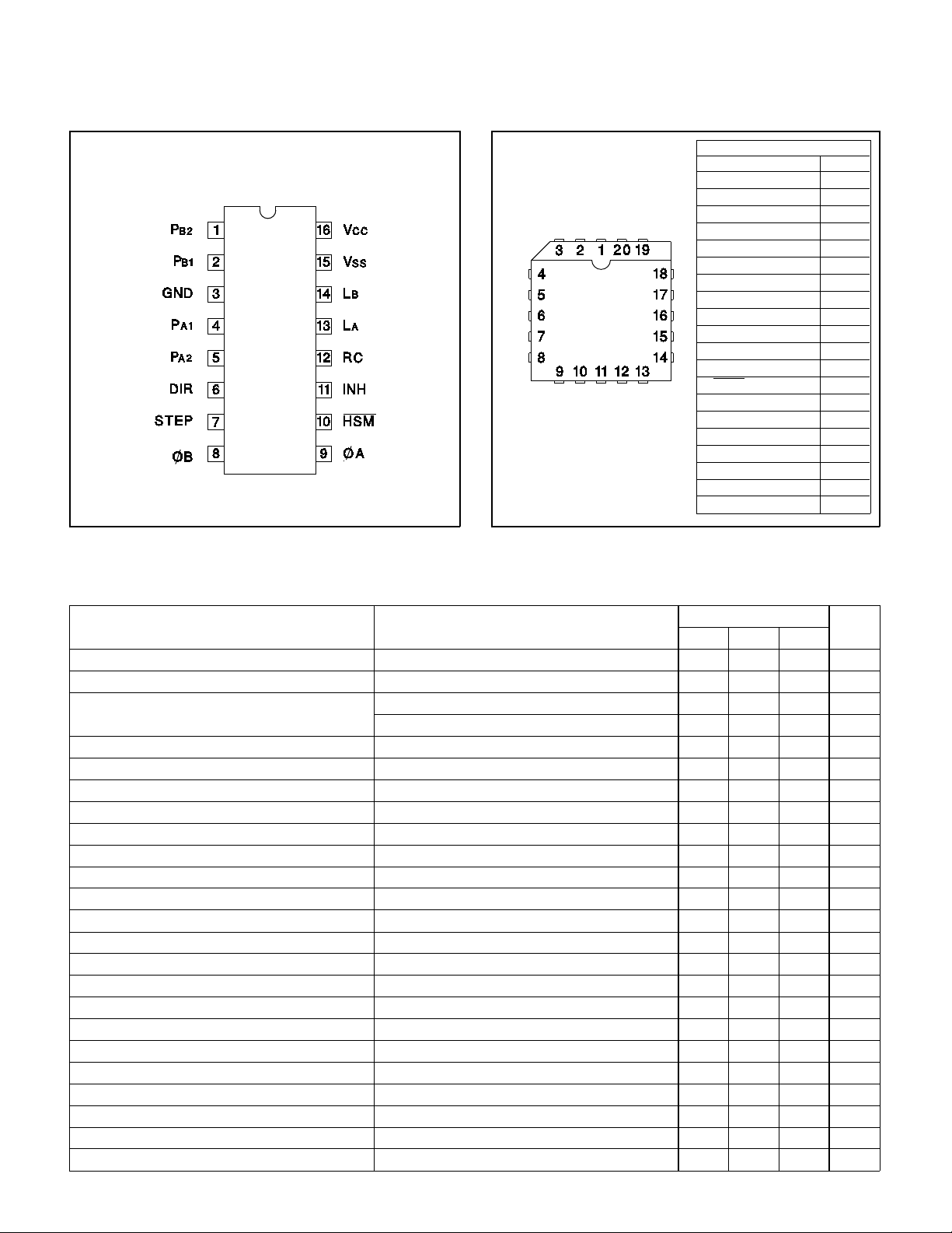
PACKAGE PIN FUNCTION
FUNCTION PIN
N/C 1
PB2 2
PB1 3
GND 4
PA1 5
N/C 6
PA2 7
DIR 8
STEP 9
ØB 10
N/C 11
ØA 12
HSM 13
INH 14
RC 15
N/C 16
LA 17
LB 18
VSS 19
VCC 20
CONNECTION DIAGRAMS
UC1517
UC3517
DIL-16 (TOP VIEW)
J or N Package
ELECTRICAL CHARACTERISTICS:
PARAMETER TEST CONDITIONS
Logic Supply, V
Second Supply, V
Logic Supply Current V
Input Low Voltage Pins 6, 7, 10, 11 0.8 V
Input High Voltage Pins 6, 7, 10, 11 2.0 V
Input Low Current Pins 6, 7, 10, 11; V = 0V -400 µA
Input High Curren t Pins 6, 7, 10, 11; V = 5V 20 µA
Phase Output Sat ura tion Voltag e Pins 1, 2, 4, 5; I = 350mA 0.6 0.85 V
Phase Output Leak age Cur re nt Pins 1, 2, 4, 5; V = 39V 500 µA
Follower Saturation Voltage to V
Follower Leakage Curre nt Pins 13,14; V = 0V 500 µA
Output Low Voltage , Ø
Phase Turn-On Time Pins 1, 2, 4, 5 2 µs
Phase Turn-Off Time Pins 1, 2, 4, 5 1 .8 µs
Second-Level On Time. T
Logic Input Set-up Time, t
Logic Input Hold Time, t
STEP Pulse Width, t
Timing Resistor Valu e Pin 12 1k 100k Ω
Timing Capacitor Value Pin 12 0.1 500 nF
Power-On Threshold Pin 16 4.3 V
Power-Off Thr eshold Pin 16 3.8 V
Power Hysteresis Pin 16 0.5 V
CC Pin 16 4.75 5.25 V
SS Pin 15 10 40 V
A, ØB Pins 8, 9; I = 1.6mA 0.1 0.4 V
MONO Pins 13,14; Figure 3 Test Circuit 275 325 375 µs
S Pins 6, 10; Figure 4 400 ns
h Pins 6, 10; Figure 4 0 ns
P Pin 7; Figure 4 800 ns
PLCC-20, LCC-20
(TOP VIEW)
Q & L PACKAGE
Unless other wise stat ed, these specif icat ions ap ply fo r TA = -55°C to +125°C for the
UC1517 and 0°C to +70°C f or the UC3517, Vcc=5 V, V
SS = 20V, TA=TJ
Pin
.
numbers refer to DIL- 16 pa ckag e.
UC1517 / UC3517 UNITS
MIN TYP MAX
INH = 0.4V 45 60 mA
V
INH = 4.0V 12 mA
SS Pins 13,14; I = 350m A -2 V
2
Page 3
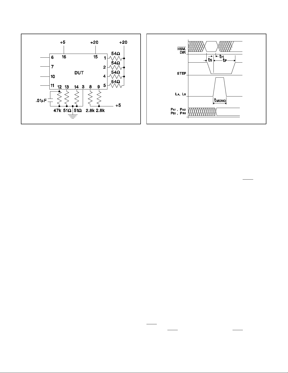
Figure 3. Test Circuit Figure 4. T im ing Waveforms
PIN DESCRIP TI ON
VCC: VCC is the UC3517’s logic supply. Connect to a
regulated 5VDC, and bypass with a 0.1µF ceramic ca-
pacitor to absorb switching transients.
MM: VMM is the primary motor supply. It connects to the
V
UC3517 phase outputs thro ugh the motor windings. Limit
this supply to less than 40V to prevent breakdown of the
phase output transistors. Select the nominal V
MM voltage
for the desired continuous winding current.
V
SS: VSS is the secondary motor supply. It drives the LA
and LB outputs of the UC35 17 w hen a mono s table in the
UC3517 is active. In the bilevel application, this supply is
applied to the motor to charge the winding inductance
faster than the primary supply could. Typically, Vss is
higher in voltage than V
than 40V. The V
SS supply should have good transient ca-
MM, al though VSS must be less
pability.
GROUND: The ground pin is the common reference for
all supplies, inputs and outputs.
RC: RC controls the timing functions of the monostables
in the UC3517. It is normally connected to a resistor (R
and a capacitor (C
Monostable on time is determined by the formula T
0.69 R
RC to V
T CT. To keep the monostabl e on indefinitely, pull
CC through a 50k resistor. The UC3517 contains
T) to ground, as shown in Figure 3.
ON ≈
only one RC pin for two monostables. If step rates comparable to T
ON are commanded, incorrect pulsing can re-
sult, so consider maximum step rates when selecting R
and CT. Keep TON ≤ T STEP MAX.
Ø
A and ØB: These logic outputs indicate half-step posi-
tion. These outputs are open-col lector, low-current drivers, and may directly drive TTL logi c. They can also drive
CMOS logic if a pull-up resistor is provided. Systems
which use the UC35 17 as an encoder and use a different
driver can use these outputs to disable the external driver,
as shown in Figure 8. The sequencing of these outputs is
shown in Figure 5.
P
A1, PA2, PB1, and PB2: The phase outputs pull to
ground sequentially to cause motor stepping, according to
the state diagram of Figure 5. The sequence of stepping
on these lines, as well as with the L
trolled by STEP input, the DIR input, and the
Caution: If these outputs or any other IC pins are pulled
too far below ground either continuously or in a transient,
step memory can be lost. I t is recommended that these
pins be clamped to ground and supply with high-speed diodes when driving inductive loads such as motor windings or solenoids. This clamping is very important
because one side of the wi nding can "ki ck" in a direction
opposite the swing of the other side.
L
A and LB: These outputs pull to VSS when their corre-
sponding monostable is active, and will remain high until
the monostable time elapses. Before and after, these outputs are high-impedance. For detail timing information,
consult Figure 5.
T)
STEP: This logic input clocks the logic in the UC3517 on
every falling edge. Like all other UC3517 inputs, this input
is TTL/CMOS compatible, and should not be pulled below
ground.
DIR: This logic input controls the motor rotation direction
by controlling the phase output sequence as shown in
Figure 5. This signal must be stable 400ns before a falling
T
edge on S TEP, and must remain stable through the edge
to insure correct stepping.
HSM: This logic input switches the UC3517 between halfsteppin g (
HSM = low) and full-stepping (HSM = high) by
controlling th e phase output sequence as show in Figure
5. This line requires the same set-up time as the DIR input, and has the same hold requirement.
UC1517
UC3517
A and LB lines is con-
HSM input.
3
Page 4

UC1517
UC3517
INH: When the inhibit i nput is high, the phase and θ out-
puts are inhibited (high impedance). STEP pulses received while inhibi ted will continue t o update logic in the
IC, but the states will not be reflected at the outputs until
inhibit is pulled low. In stepper motor systems, this can be
used to save power or to allow the rotor to move freely for
manual repositioning.
OPERATING MODES
The UC3517 is a system component capable of many different operating modes, including:
Unipolar Stepper Driver: In its simplest form, the
UC3517 can be connected to a stepper motor as a unipolar driver. L
left open. All other system design considerations mentioned above apply, including choice of motor supply
VMM, undershoot diodes and timing considerations.
Unipolar Bilevel Stepper Driver: If increased step rates
are desired, the ap plicatio n ci rcuit of Figure 6 makes use
of the monostables and emitter followers as well as the
configuration mentioned above to provide high-voltage
pulses to the motor windings when the phase is turned
on. For a given dissipation level, this mode offers faster
step rates, and very little additional electrical noise.
The choice of monostable co mponents can be estimated
based on the timing relationship of motor current and voltage: V = Ldl/dt. Assuming a fixed secondary supply voltage (V
winding peak current (I
tor, we can estimate that R
practice, these calculations should be confirmed and adjusted to accommodate for effect s not modeled.
V oltage-Dou bled Mo de: The UC3517 can also be used
to generate higher vol tages than available with the system power supplies using capacitors and diodes. Figure 9
shows how this might be done, and gives some estimates
for the component values.
Higher Current O peratio n : For systems requiring more
than 350mA of drive per phase, the UC3717A can be
A, LB, RC and Vss are not used, and may be
SS), a fixed winding inductance (LM), a desired
W), and no back EMF from the mo-
TCT = 1.449 IWLM/VSS. In
used in conjunction with discrete power transistors or
power driver ICs, like the L298. These can be connected
as current gain devices that turn on when the phase outputs turn on.
Bipolar Mot or D riv e: Bipolar motors can be controlled by
the UC3517 with the addition of bipolar integrated drivers
such as the UC3717A (Figure 8) and the L298, or discrete
devices. Care should be taken with discrete devices to
avoid potential cross-conduction prob lems.
LOGIC FLOW GRAPH
The UC3517 con tains a bi directional counter which is decoded to generate the correct phase and Ø outputs. This
counter is incremented on every falling edge of the STEP
input. Figure 5 shows a graph representing the counter
sequence, inputs that determine the next state (DIR and
HSM), and the outputs at each state. Each circle represents a unique logic state, and the four inside circles represent the half-step stat es.
The four bits inside the circl es represent the phase outputs in each state (P
the circle label ed 1010 is immediatel y entered when the
device is powered up, and represents P
high), P
A2 on ("0" or low), PB1 off ("1" or high) and PB2 on
("0" or low). The Ø
tified).
The arrows in the graph show the state chan ges. For example, if the IC is in state 0110, DIR is high,
and STEP falls, the next state will be 0101, and a pulse
will be generated on the L
Inhibit will not effect the logic state, but it will cause all
phase outputs and both Ø outputs to go high (off). A fall-
ing edge o n STEP will still cause a state change, but inhibit will have to toggle low for the state to be apparent.
A falling edge on STEP with
counter to advance to the next full step state regardless
of whether or not it was in a full step state previously.
No L
A or LB pulses ar e generated entering half-states.
A1, PA2, PB1, and PB2). For example,
A1 off ("1" or
A and ØB outputs are both low (uniden-
HSM is high,
B line by the monostable.
HSM high will cause the
4
Page 5

UC1517
UC3517
Figure 5. Logic Flow Graph
For applications requiring very fast step rates, a zener diode
permits windings to discharge at higher voltages, and higher
rates. Driver transistor breakdown must be considered when
selecting Vss and zener voltage to insure that the outputs will
not overshoot past 40V. I f the zener diodes are not used and
UC3610 pin 2 is connected directly to Vss then higher Vss can
be used.
Figure 6. Bilevel Motor Driver
5
Page 6
UC1517
UC3517
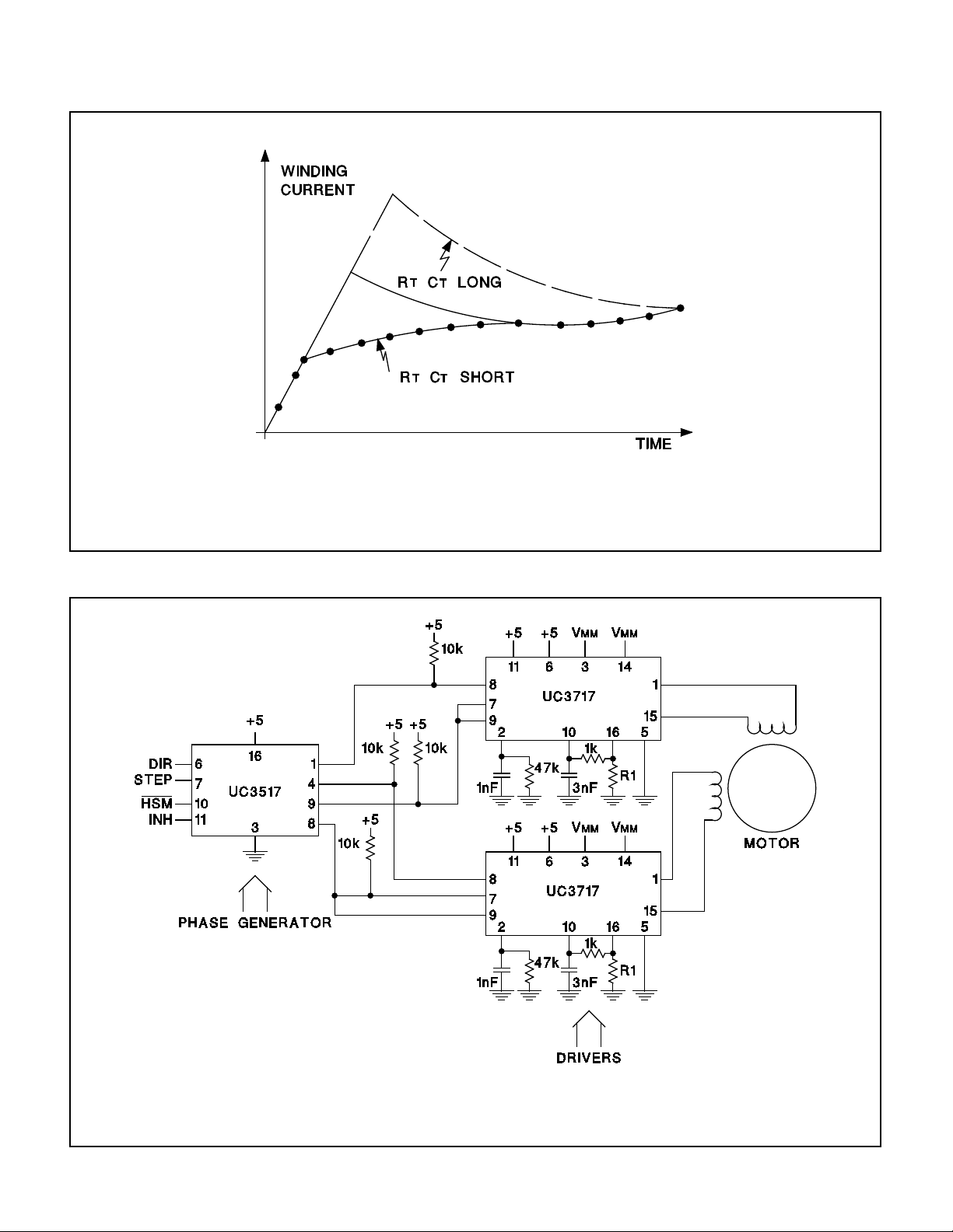
Experimental selection of RT and CT allow the designer to select a small amount of winding current overshoot, as shown
above. Although the overshoot may exceed the continuous
rated current of the winding and the drive transistors, the dura-
Figure 7. E ffects of Different RT & CT on Bilevel Sys tems
tion can be well controlled. Average power dissipation for the
driver and motor must be considered when designing systems with intentional overshoot, and must stay within conservative limits for short duty cycles.
In this application, the ∅A and ∅B o utputs of the UC3517 are
connected to the current program inputs of the UC3717. This
allows the UC3517 inhibit signal to inhibit the UC3717, and
Figure 8. I nt erf ace to UC371 7 Bipolar Dr iv er
also allows half-step operation of the UC3717. Peak motor
winding current will be limited to approximately .42V/R1 by
chopping.
6
Page 7

UC1517
UC3517
Although compo nent value s can be best opt imize d expe riment ally, good starting values speed developm ent . For this des ign,
start with: where:
RT CT = 3 LW/RW LW is winding inductance,
C
1 = C2 = LW IR/RW RW is winding resistance,
R
1 = R2 = 2.9 TMIN/C1 IR is rated winding current, and
T
MIN
is minimum step period expected.
Figure 9. Using the UC3517 as a Volt age Doubler
UNITRODE INTEGRATED CIRCUITS
7 CONTINENTAL BLVD. •• MERRIMACK, NH 03054
TEL. (603) 424-2410 •• FAX (603) 424-3460
7
Page 8

IMPORTANT NOTICE
T exas Instruments and its subsidiaries (TI) reserve the right to make changes to their products or to discontinue
any product or service without notice, and advise customers to obtain the latest version of relevant information
to verify, before placing orders, that information being relied on is current and complete. All products are sold
subject to the terms and conditions of sale supplied at the time of order acknowledgement, including those
pertaining to warranty, patent infringement, and limitation of liability.
TI warrants performance of its semiconductor products to the specifications applicable at the time of sale in
accordance with TI’s standard warranty. Testing and other quality control techniques are utilized to the extent
TI deems necessary to support this warranty . Specific testing of all parameters of each device is not necessarily
performed, except those mandated by government requirements.
CERTAIN APPLICA TIONS USING SEMICONDUCT OR PRODUCTS MAY INVOLVE POTENTIAL RISKS OF
DEATH, PERSONAL INJURY, OR SEVERE PROPERTY OR ENVIRONMENTAL DAMAGE (“CRITICAL
APPLICATIONS”). TI SEMICONDUCTOR PRODUCTS ARE NOT DESIGNED, AUTHORIZED, OR
WARRANTED TO BE SUITABLE FOR USE IN LIFE-SUPPORT DEVICES OR SYSTEMS OR OTHER
CRITICAL APPLICA TIONS. INCLUSION OF TI PRODUCTS IN SUCH APPLICATIONS IS UNDERST OOD TO
BE FULLY AT THE CUSTOMER’S RISK.
In order to minimize risks associated with the customer’s applications, adequate design and operating
safeguards must be provided by the customer to minimize inherent or procedural hazards.
TI assumes no liability for applications assistance or customer product design. TI does not warrant or represent
that any license, either express or implied, is granted under any patent right, copyright, mask work right, or other
intellectual property right of TI covering or relating to any combination, machine, or process in which such
semiconductor products or services might be or are used. TI’s publication of information regarding any third
party’s products or services does not constitute TI’s approval, warranty or endorsement thereof.
Copyright 1999, Texas Instruments Incorporated
 Loading...