

United Monolithic Semiconductors CND2050-DAF-20 Datasheet
0.5-11.5 GHz Divide by 4 Static Prescaler
GaAs Monolithic Microwave IC
Description
The CND2050 is a low power consumption
and very high speed divider by 4
manufactured with a 0.6µm GaAs self
aligned implanted MESFET process.
The design is full differential input/output
that allows direct drive into 50Ω load.
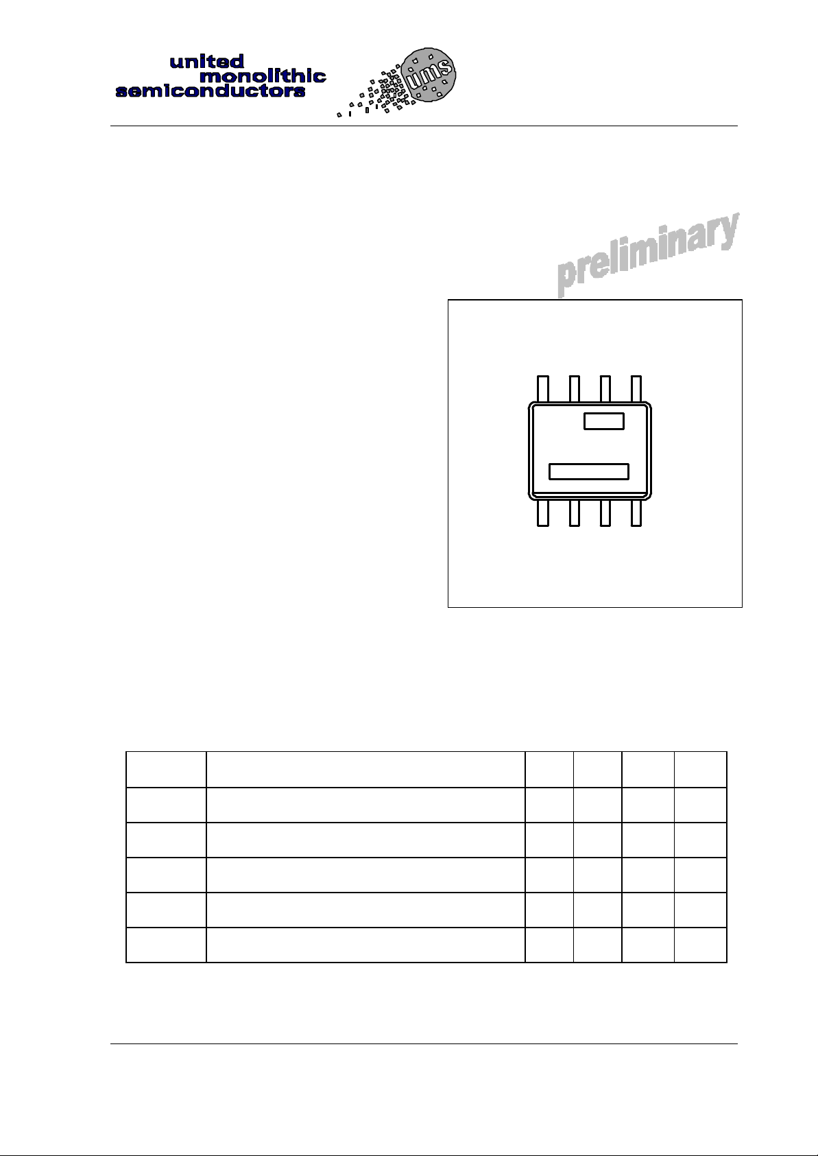
The CND2050 is available in SOIC8
package form .
CND2050
UMS
CND2050
Main Features
Very broad operating frequency range
Low power dissipation: 250mW
Single supply operation:+ 5V or –5V
High input sensitivity:
-10dBm@10 GHz at 25°C
Low phase noise: -139dBc/Hz at 1KHz
SOIC8 plastic package
Main Characteristics
at Tamb= +25°C
Symbol Parameter Min Typ Max Unit
Vdd Bias supply (with Vss = 0) 3.3 5 6 V
Vss Bias supply (with Vdd = 0) -6 -5 -3.3 V
Pdiss Power dissipation 90 250 350 mW
Fmin Minimum input frequency 0.5 GHz
Fmax Maximum input frequency (Vdd=5V) 10 12 GHz
ESD Protections: Electrostatic discharge sensitive device. Observe handling precautions!
Ref. : DSCND20500257 -13-Sep.-00 1/9 Specifications subject to change without notice
United Monolithic Semiconductors S.A.S.
Route Départementale 128 - B.P.46 - 91401 Orsay Cedex France
Tel. : +33 (0)1 69 33 03 08 - Fax : +33 (0)1 69 33 03 09
CND2050
0.5-10GHz frequency divider by 4
Electrical Characteristics (1)
Guaranteed electrical specifications at +25°C
Tested under configuration described in Fig.1 and Fig.2
Vdd = 5V , Vss = 0 ; Pin = 0 dBm ; Zo = 50 Ω
Symbol Parameter Min Typ Max Unit
Fmin Minimum input frequency
(Differential or single input)
Fmax Maximum input frequency
differential input
single input
Pout Minimum output power
(Differential or single input) -5 -2 dBm
Guaranteed electrical specifications at +25°C
Tested under configuration described in Fig.1
Differential inputs ; Vss = 0 ; Pin = 0 dBm ; Zo = 50 Ω
Symbol Parameter Min Typ Max Unit
Fmin Minimum input frequency
Vdd = 3.3 to 5 V 0.5 GHz
10
9
12
11
0.5 GHz
GHz
GHz
Fmax Maximum input frequency
Vdd = 5V
Vdd = 3.3V
Pout Minimum output power
Vdd = 5V
Vdd =3.3V
Ref. : DSCND20500257 -13-Sep.-00 2/9 Specifications subject to change without notice
United Monolithic Semiconductors S.A.S.
Route Départementale 128 - B.P.46 - 91401 Orsay Cedex France
Tel. : +33 (0)1 69 33 03 08 - Fax : +33 (0)1 69 33 03 09
10
9
-5
-10
12
11
-2
-7
GHz
GHz
dBm
dBm
0.5-11.5 GHz Divide by 4 prescaler
CND2050
Electrical Characteristics (2)
Guaranteed electrical specifications over the temperature range of -40°C to +85°C
Tested under configuration described in Fig.1
Differential inputs ; Vss = 0 ; Pin = 0 dBm ; Zo = 50 Ω
Symbol Parameter Min Typ Max Unit
Fmin Minimum input frequency
Vdd = 3.3 to 5 V 0.5 GHz
Fmax Maximum input frequency
Vdd = 5V
Vdd = 3.3V
Pout Minimum output power
Vdd = 5V
Vdd =3.3V
Guaranteed electrical specifications over the temperature range of -40°C to +85°C
Single or differential inputs ; Vss = 0 ; Zo = 50 Ω
Symbol Parameter Min Typ Max Unit
Pin max Maximum operational input power
Vdd = 3.3 to 5 V 10 dBm
9
8
-6
-11
11
10
-3
-8
GHz
GHz
dBm
dBm
Idd Supply current
Vdd= 5V
Vdd=3.3V
Hr Harmonic rejection (ouput signal) 10 dBc
Ref. : DSCND20500257 -13-Sep.-00 3/9 Specifications subject to change without notice
Route Départementale 128 , B.P.46 - 91401 ORSAY Cedex - FRANCE
Tel.: +33 (0)1 69 33 03 08 - Fax : +33 (0)1 69 33 03 09
35
20
45
25
70
40
mA
mA
 Loading...