

United Monolithic Semiconductors CHX1094-99F-00 Datasheet
12-36GHz Frequency Multiplier
GaAs Monolithic Microwave IC
Description
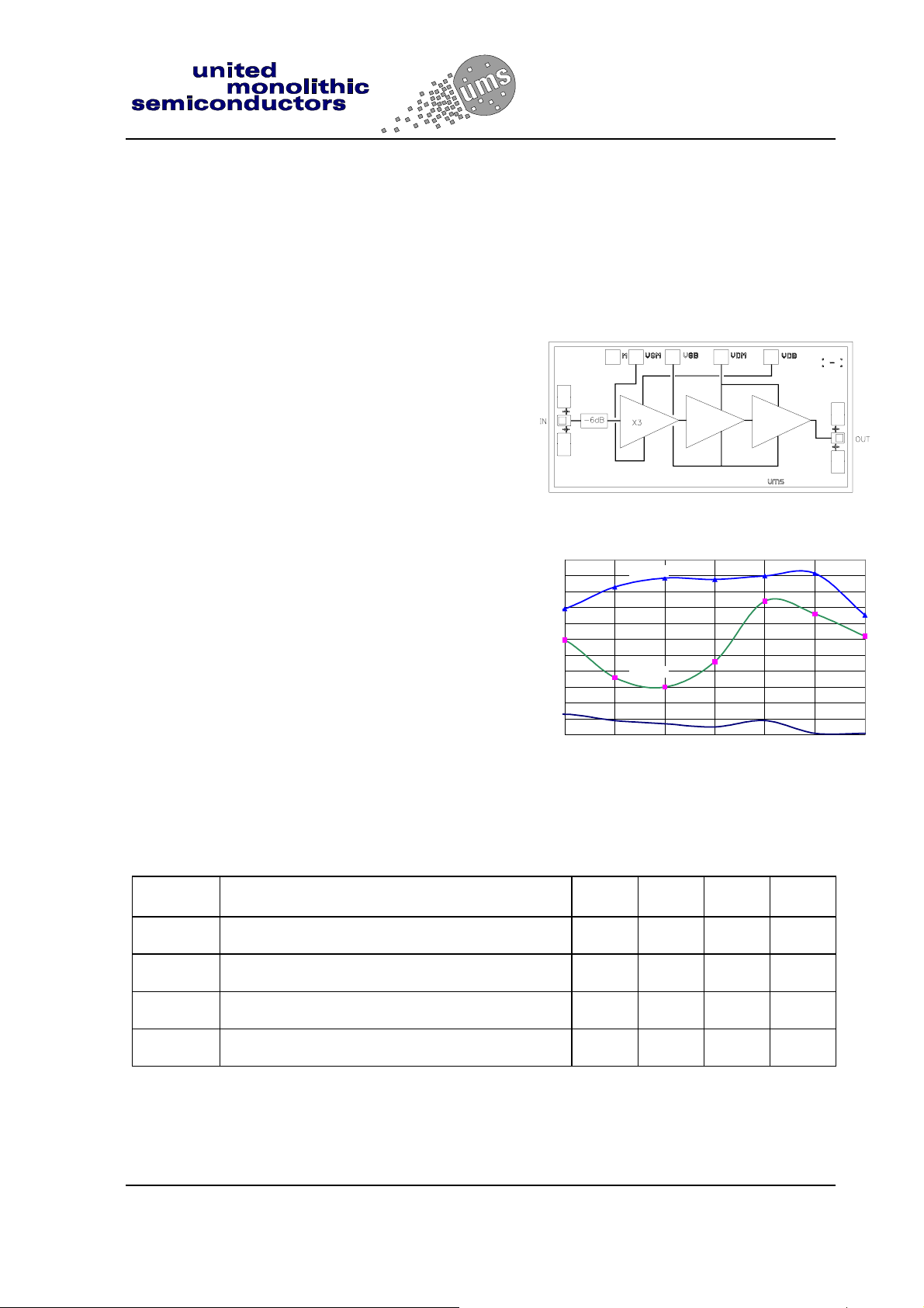
The CHX1094 is a cascadable frequency
multiplier by 3 monolithic circuit.
It is designed for a wide range of applications,
from military to commercial communication
systems. The backside of the chip is both RF
and DC grounds. This helps simplify the
assembly process.
The circuit is manufactured with a P-HEMT
process, 0.25µm gate length, via holes through
the substrate, air bridges and electron beam
gate lithography.
Main Features
■ Broadband performances : 12-13.5GHz
■ 10dBm output power for +14dBm input power
■ DC bias : Vd=3.Volt @Id=60mA
■ Chip size : 2.07 x 1.03 x 0.10 mm
CHX1094
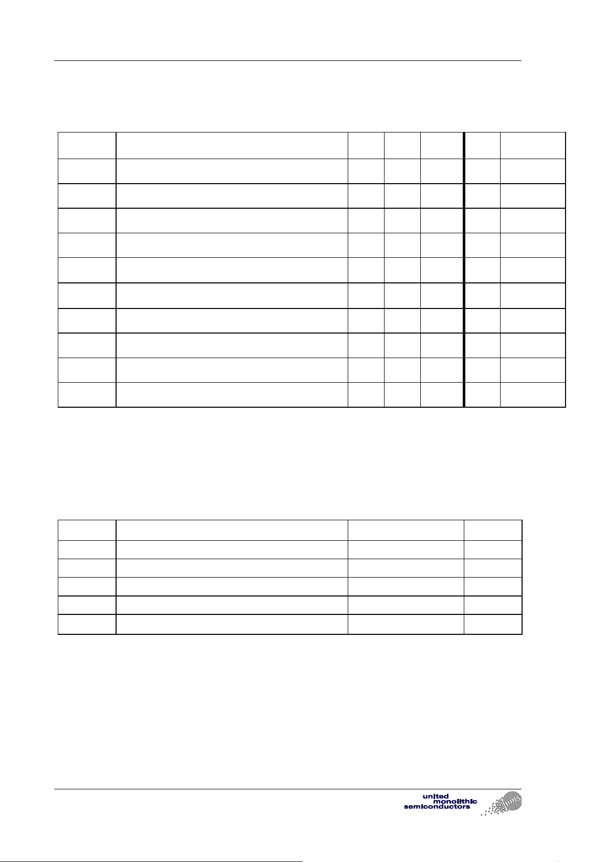
15.0
10.0
5.0
0.0
-5.0
-10.0
-15.0
-20.0
Output power (dBm)
-25.0
-30.0
-35.0
-40.0
11 11.5 12 12.5 13 13.5 14
P ( 3*Fin )
P ( 2*Fin )
P ( Fin )
Input Frequency (GHz)
typical measurement
Main Characteristics
Tamb. = 25°C
Symbol Parameter Min Typ Max Unit
Fin Input frequency range 12 13.5 GHz
Fout Output frequency range 36 40.5 GHz
Pin Input power 14 dBm
Pout Output power @ Pin= 14dBm 10 dBm
ESD Protection : Electrostatic discharge sensitive device. Observe handling precautions !
Ref. : DSCHX10941071 -12-Mar.-01
United Monolithic Semiconductors S.A.S.
Route Départementale 128 - B.P.46 - 91401 Orsay Cedex France
Tel. : +33 (0)1 69 33 03 08 - Fax : +33 (0)1 69 33 03 09
1/4
Specifications subject to change without notice
CHX1094
12-36GHz Frequency Multiplier
Electrical Characteristics
Tamb = +25°C, Vgm = -1.5V , Vgb = -0.2V.
Symbol Parameter Min Typ Max Typ Unit
Fin Input frequency range 12 13.5 14 GHz
Fout Output frequency range 36 40.5 42 GHz
Pin Input power 12 14 16 16 dBm
Pout Output power @ Pin=14dBm 8 10 5 dBm
H3/H2
H3/H1
VSWRin Input VSWR 2:1 2:1
VSWRout Output VSWR 2.5:1 2.5:1
Vd DC voltage 2.5 3.5 4 V
Id Bias current 60 80 80 mA
nd
Harmonic rejection ( Pin ≤ 14dBm)
2
Fund. rejection ( Pin ≤ 14dBm)
810 5 dBc
30 35 dBc
Absolute Maximum Ratings
Tamb. = 25°C (1)
Symbol Parameter Values Unit
Vd Drain bias voltage 4.5 V
Id Drain bias current 120 mA
Vg Gate bias voltage -2 to +0.4 V
Ta Operating temperature range -40 to +85 °C
Tstg Storage temperature rang e -55 to +155 °C
(1) Operation above anyone of these parameters may cause permanent damage of this device.
Ref. : DSCHX10941071 -12-Mar.-01
Route Départementale 128 , B.P.46 - 91401 ORSAY Cedex - FRANCE
Tel.: +33 (0)1 69 33 03 08 - Fax : +33 (0)1 69 33 03 09
2/4
Specifications subject to change without notice
 Loading...