


United Monolithic Semiconductors CHV2243-99F-00 Datasheet
CHV2243
Fully Integrated Q-band VCO
based on Ku-band Oscillator and Q-band Multiplier
GaAs Monolithic Microwave IC
Description
The CHV2243 is a monolithic multifunction
for frequency generation. It integrates a
Ku-band oscillator with frequency control
(VCO), a Q-band frequency multiplier and
buffer amplifiers. The VCO is fully
integrated. On chip P-HEMT based
Schottky diode is used as varactor. All the
active devices are internally self biased.
The circuit is manufactured with the PHEMT process : 0.25µm gate length, via
holes through the substrate, air bridges
and electron beam gate lithogr aphy.
It is available in chip form.
Main Features
n Ku-band VCO + Q-band multiplier
n Fully integrated VCO
n Wide f r equency tuning range
n PLL oriented
n Auxiliary output at VCO frequency
n High temperature rang e
n On-chip self biasing
n Automatic assembly oriented
n Chip size 2.41 x 1.18 x 0.1 mm
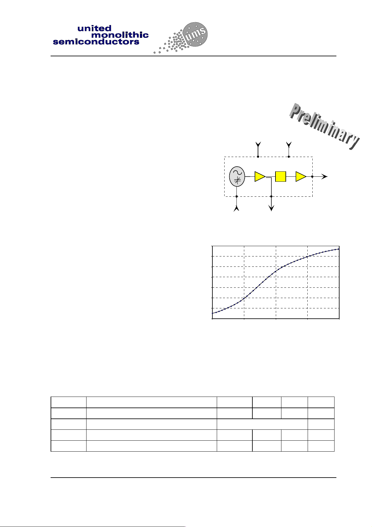
+V -V
F_VCO = F_out/3
x3
V_tune
Multifunction block diagram
40
39,5
39
38,5
38
37,5
Output frequency (GHz)
37
36,5
0 0,5 1 1,5 2
Typical tuning characteristic
VCO_out_aux
Tuning voltage (V)
RF_out
(F_out)
Main Characteristics
Tamb = +25°C
Symbol Parameter Min Typ Max Unit
F_out Out put centre frequency 38 38.25 38.5 GHz
F_vco Oscillator frequency F_out/3
F_tune1 Output frequency tuning range 1.5 3 GHz
Pout Output power 5 7 dBm
ESD Protections : Electrostatic discharge sensitive device observe handling precautions !
Ref. : DSCHV22431074 -15-Mar.-01 1/6 Specifications subject to change without notic e
united monolithic semiconductors S.A.S.
Route Départementale 128 - B.P.46 - 91401 Orsay Cedex France
Tel. : +33 (0)1 69 33 03 08 - Fax : +33 (0)1 69 33 03 09
CHV2243
Q-band VCO
Electrical Characteristics
Full temperature range, used accor ding to section “Typical assembly and bias configurat ion”
Symbol Parameter Min Typ Max Unit
F_out Output centre frequency 38 38.25 38.5 GHz
F_vco VCO frequency F_out/3
F_tune1 Maximum f r equency tuning range (@ F_out) 1.5 3 4 GHz
F_tune2 Specif ied frequency tuning range (@ F_out)
(1)
∆F_tune2(T)
P_out Output power on RF_out port 5 7 12 dBm
H1 Sub-harmonics rejection (Fout/3) (2) -16 -11 dBc
H2 Sub-harmonics rejection (2*Fout/3) (2) -17 -12 dBc
P_VCO VCO output power on VCO_out_aux port (4) tbd
V_tune Control voltage range 0.5-1 0 - 2 V
F_slope Fr equency tuning slope (2) 1000 2800 4500 MHz/v
∆F_slope(T)
P_V+ Frequency pushing vs positive supply
P_V- Frequency pushing vs negative supply
PN Phase noise (given at F_out) (2)
+V Positive supply voltage (3) 4.4 4.5 4.6 V
+I Positive supply current 130 180 mA
-V Negative supply voltage (3) -4.6 -4.5 -4.4 V
-I Negative supply current 4 8 mA
Top Operating temperature r ange -40 +100 °C
Maximum variation of Frequency over
temperature (2)
Maximum variation of Frequency tuning
slope over temperature (2)
voltage (2)
voltage (2)
@ 1kHz
@ 10kHz
@ 100kHz
@ 200kHz
@ 1MHz
200 300 500 MHz
-300 +300 MHz
-26 +34 %
150 450 MHz/v
80 250 MHz /v
-5
-35
-65
-73
-92
+5
-25
-55
-63
-82
dBc/Hz
(1) F_tune2 is the frequency tuning range relative to the specified parameters, this
frequency tuning range has to be inside 38 to 38.5GHz.
(2) Specified within F_tune2
(3) Negative supply voltage must be applied at least 1µs before positive supply
voltage
(4) This output is optional, it can be not connected
Ref. : DSCHV22431074 -15-Mar.-01 2/6 Specifications subject to change without notic e
Route Départementale 128 , B.P.46 - 91401 ORSAY Cedex - FRANCE
Tel.: +33 (0)1 69 33 03 08 - Fax : +33 (0)1 69 33 03 09