

United Monolithic Semiconductors CHR2295-99F-00 Datasheet
Q
24-30GHz Integrated Down Converter
GaAs Monolithic Microwave IC
Description
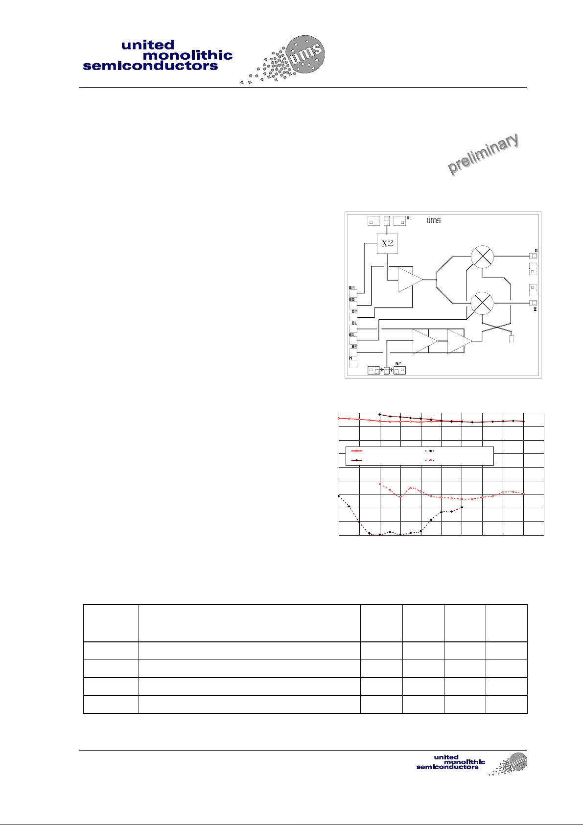
The CHR2295 is a multifunction chip which
integrates a LO time two multiplier, a balanced
cold FET mixer, and a RF LNA. It is des igned for
a wide range of ap plic ati on s , t ypical l y com mercial
communication systems. The backside of the
chip is both RF and DC grounds. This helps
simplify the assembly process.
The circuit is manufactured with a PM-HEMT
process, 0.25µm gate length, via holes through
the substrate, air bridges and electron beam
gate lithography.
It is available in chip form.
Main Features
• Broadband performances : 24-30GHz
• 11 dB conversion gain
• 3.5.0dB noise figure
• 10dBm LO input power
• -10dBm RF input power (1dB gain comp.)
• Low DC power consumption, 120mA@3.5V
• Chip size : 2.49 X 1.97 X 0.10 mm
Main Characteristics
Tamb. = 25°C
Parameter Min Typ Max Unit
CHR2295
GM
GB
VDM
VDL
GX
VGA
12.00
8.00
4.00
0.00
-4.00
(dB)
-8.00
-12.00
-16.00
-20.00
-24.00
22.5 23.5 24.5 25.5 26.5 27.5 28.5 29.5 30.5 31.5 32.5
Conversion Gain & Image suppression @ IF=1.5GHz
LO
RF
Gc_channel_sup_rf+ Gc_channel_inf_rf+
Gc_channel inf_rf- Gc_channel_sup_rf-
2XLO Frequency (GHz)
(including test board losses)
I
FRF RF frequency range 24 30 GHz
FLO LO frequency range 12 15 GHz
FIF IF frequency range 0.25 1.5 GHz
Gc Conversion gain 11 dB
ESD Protection : Electrostatic discharge sensitive device. Observe handling precautions !
Ref. : DSCHR22951201 -20-July-01 1/6 Specifications subject to change without notice
Route Départementale 128 , B.P.46 - 91401 ORSAY Cedex - FRANCE
Tel.: +33 (0)1 69 33 03 08 - Fax : +33 (0)1 69 33 03 09
24-30GHz MFC Down Converter
CHR2295
Electrical Characteristics for Broadband Operation
Tamb = +25°C, Vd = 3.5V
Symbol Parameter Min Typ Max Unit
FRF RF frequency range 24 30 GHz
FLO LO frequency range 12 15 GHz
FIF IF frequency range 0.25 1.5 GHz
Gc Conversion gain (1) 11 dB
NF Noise Figure 3.5 dB
PLO LO Input power +10 dBm
Img Sup Image Suppression 17 dBc
P1dB Input power at 1dB gain compression -10 dBm
LO VSWR Input LO VSWR (1) 2.0:1
RF VSWR Input RF VSWR (1) 3.0:1
Id Bias current (2) 120 mA
(1) On Wafer measurements
(2) Current source biasing network is recommended. Optimum performances for Idm= 50mA
and Idl= 70mA
Absolute Maximum Ratings
Tamb. = 25°C (1)
Symbol Parameter Values Unit
Vd Drain bias voltage 4.0 V
Id Drain bias current 200 mA
Vg Gate bias voltage -2.0 to +0.4 V
Pin Maximum peak input power overdrive (2) +15 dBm
Ta Operating temperature range -40 to +85 °C
Tstg Storage temperature range -55 to +155 °C
(1) Operation of this device above anyone of these parameters may cause permanent damage.
(2) Duration < 1s.
Ref. : : DSCHR22951201 -20-July-01 2/6 Specifications subject to change without notice
Route Départementale 128 , B.P.46 - 91401 ORSAY Cedex - FRANCE
Tel.: +33 (0)1 69 33 03 08 - Fax : +33 (0)1 69 33 03 09
 Loading...