

United Monolithic Semiconductors CHA7010-99F-00 Datasheet
X-band GaInP HBT High Power Amplifier
GaAs Monolithic Microwave IC
Description
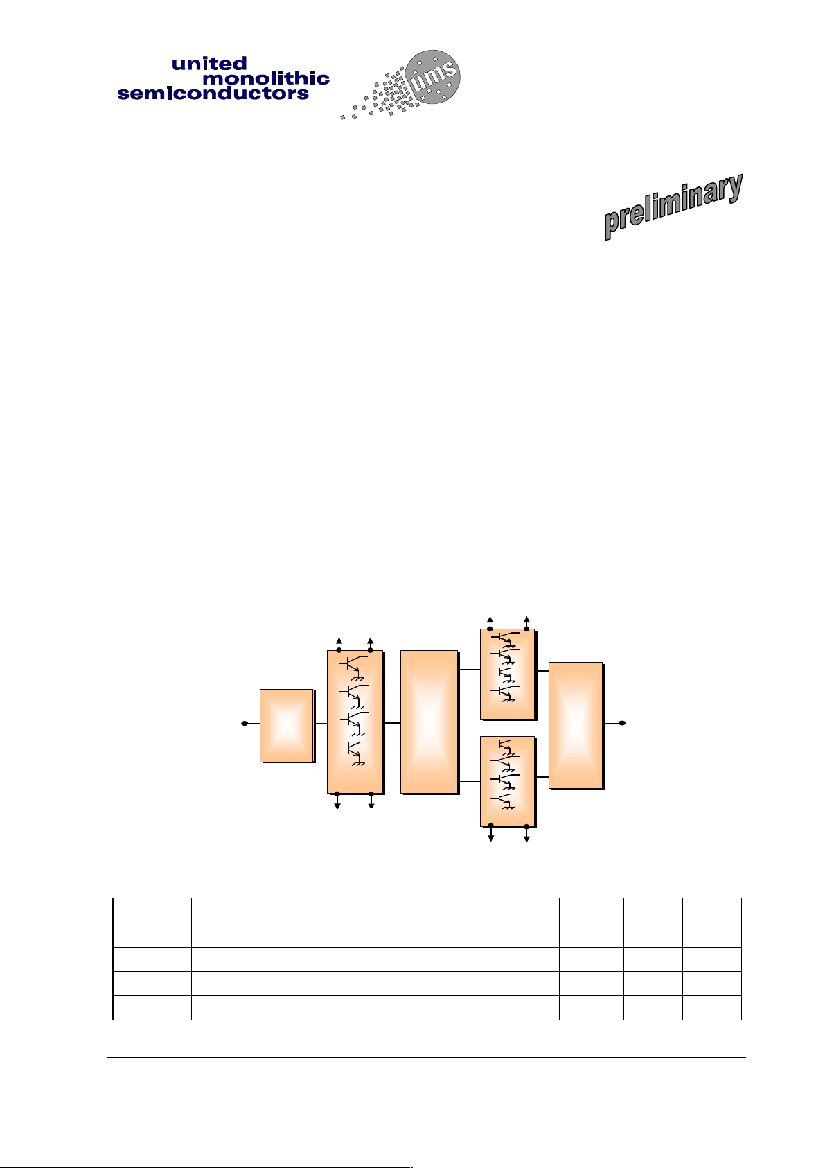
The CHA7010 is a monolithic two stage
GaAs high power amplifier designed f or X
band applications.
This device is manufactured using a GaInP
HBT process, including, via holes through
the substrate and air bridges. A nitride
layer protects the transistors and the
passive components. Special heat removal
techniques are implemented to guarantee
high reliability.
To simplify the assembly process;
• the backside of the chip is both RF and
DC grounded
• bond pads and back side are gold
plated for compatibility with eutectic die
attach method and thermo-sonic or
thermo-compression bonding process.
Vctr
Vc
CHA7010
Main Features
n 10W output power
n High gain : > 18dB @ 10GHz
n High PAE : > 35% @ 10GHz
n On-chip bias control
n Linear collector current control
n High impedance interface for pulse
mode
n Temperature compensated
n Chip size: 4.74 x 4.36 x 0.1 mm
Vctr Vc
Vc
Inter-stage
Vctr
Vc
Output
Combiner
Input
Matching
Network
Vctr
Main Characteristics
Tamb = +25°C
Symbol Parameter Min Typ Max Unit
F_op Operat ing frequency range 8.4 9.4 10.4 GHz
P_sat Saturated output power 10 W
P_1dBc Output power @ 1dBc 8 W
G_lin Linear gain 18 dB
ESD Protections : Electrostatic discharge sensitive device observe handling precautions !
Ref. : DSCHA70102175 -24-June-02 1/7 Specifications subject to change without notic e
United Monolithic Semiconductors S.A.S.
Route Départementale 128 - B.P.46 - 91401 Orsay Cedex France
Tel. : +33 (0)1 69 33 03 08 - Fax : +33 (0)1 69 33 03 09
X-band High Power Amplifier
CHA7010
Electrical Characteristics
Tamb = 25°C, Vc=9V, Vctr=5.5V, Pulse width=80µs , Duty cycle = 30%
Symbol Parameter Min Typ Max Unit
F_op
G_lin_1
G_lin_2
G_lin_T
RL_in
RL_out
P_sat_1
P_sat_2
P_sat_T
Operating freq uency 8.4 9.4 10.4 GHz
Linear gain (8.4 to 9.4GHz) 14 16 dB
Linear gain (9.4 to 10.4GHz) 16 18 dB
Linear gain variation versus temperature -0.035 dB/°C
Input Return Loss 8 12 dB
Output Return Loss 6 12 dB
Saturated output power (8.4 to 9.8G Hz) 39 40 dBm
Saturated output power (9.8 to 10.4G Hz) 38 39 dBm
Saturated output power variation versus
-0.01 dB/°C
temperature
P_1dBc_1
P_1dBc_2
PAE_sat
PAE_1dBc
Vc
Ic
Vctr
Zctr
Top
Output power @ 1dBc (8.4 to 9.8GHz) 38 39 dBm
Output power @ 1dBc (9.8 to 10.4GHz) 37 38 dBm
Power Added Efficiency in saturation 30 35 %
Power Added Efficiency @ 1dBc 27 32 %
Power supply voltage 9 V
Power supply quiescent current (1) 2.4 A
Collector current control voltage 5.5 V
Vctr input port impedance (2) 350 Ohm
Operating temperature r ange (3) -30 +80 °C
(1) This parameter is fixed by Vctr
(2) This value corresponds to the 4 ports in parallel (Pin 4, 9, 17, 22)
(3) The reference is the back-side of the chip
Absolute Maximum Ratings (1)
Tamb = 25°C
Symbol Parameter Values Unit
Cmp Compression level 6 dB
Vc Power supply voltage 10 V
Ic Power supply quiescent current 2.8 A
Ic_sat Power supply current in saturation 3.5 A
Vctr Collector curr ent control voltage 6.5 V
Tstg Storage temperature range -55 to +125 °C
(1) Operation of this device above anyone of these parameters may cause permanent damage.
Ref. : DSCHA70102175 -24-June-02 2/7 Specifications subject to change without notic e
Route Départementale 128 , B.P.46 - 91401 ORSAY Cedex - FRANCE
Tel.: +33 (0)1 69 33 03 08 - Fax : +33 (0)1 69 33 03 09

X-band High Power Amplifier
Typical measured characteristics
Measurements in test fixture :
Tamb=25°C, Vc=9V, Vctr=5.5V, Pulse width=80µs , Duty cycle = 30%
20
16
12
8
CHA7010
S21, S11, S22 (dB)
42
40
38
36
4
0
-4
-8
-12
-16
-20
8 8,5 9 9,5 10 10,5 11 11,5 12
db(S21)
db(S11)
db(S22)
Frequency(GHz)
S-parameters
34
32
30
Output power (dBm)
28
26
24
22
-101234567
Compression level (dB)
Pout @ 8,4 GHz
Pout @ 8,6 GHz
Pout @ 8,8 GHz
Pout @ 9 GHz
Pout @ 9.2 GHz
Pout @ 9.4 GHz
Pout @ 9.6 GHz
Pout @ 9.8 GHz
Pout @ 10 GHz
Pout @ 10.2 GHz
Pout @ 10.4 GHz
Output power versus compression level : F= 8.4 to 10.4GHz
Ref. : DSCHA70102175 -24-June-02 3/7 Specifications subject to change without notic e
Route Départementale 128 , B.P.46 - 91401 ORSAY Cedex - FRANCE
Tel.: +33 (0)1 69 33 03 08 - Fax : +33 (0)1 69 33 03 09
 Loading...