

United Monolithic Semiconductors CHA5215aFKF-23, CHA5215a99F-00 Datasheet
Description
CHA5215a
5.8GHz Medium Power Amplifier
GaAs Monolithic Microwave IC
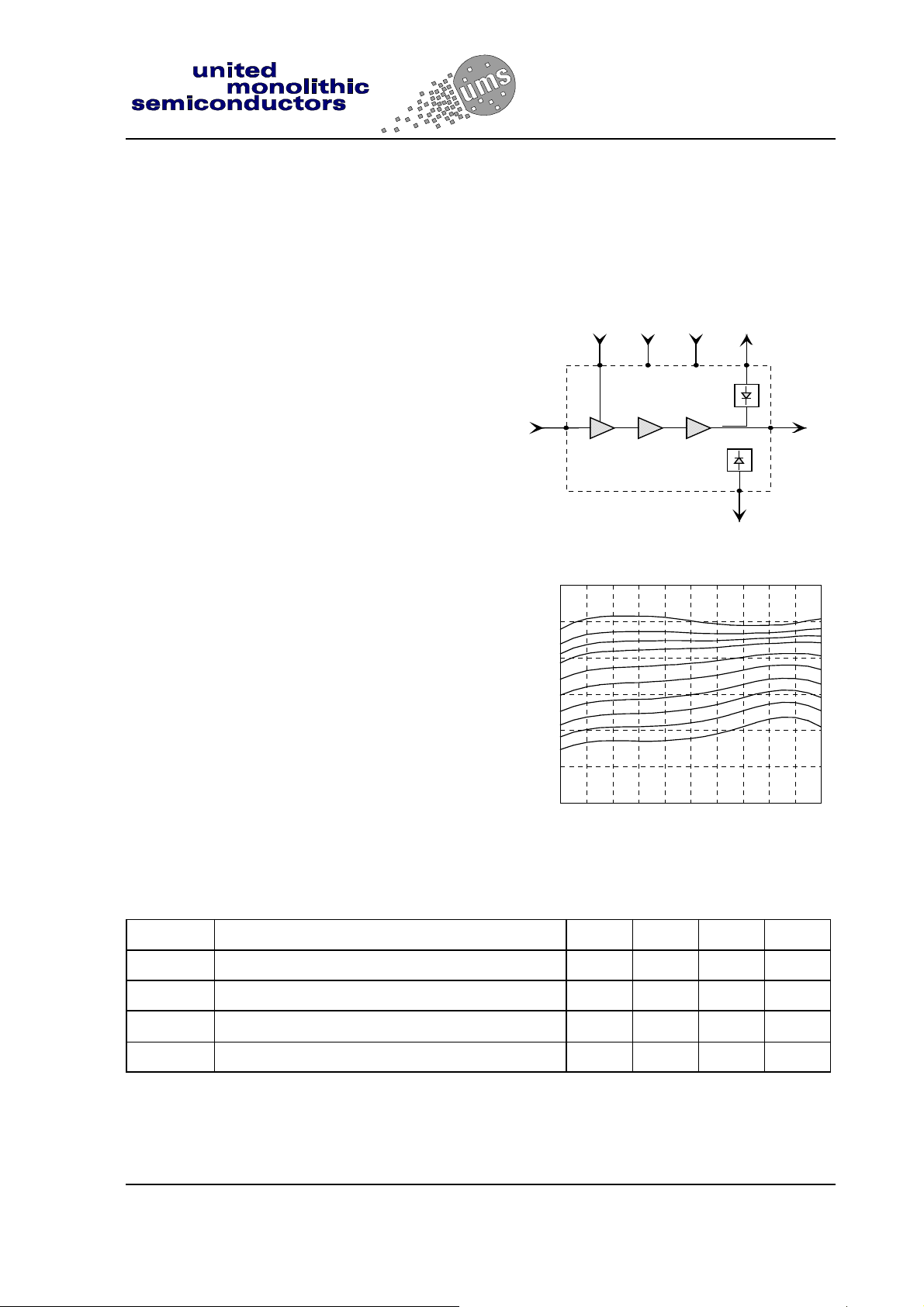
The CHA5215a is a MMIC multifunction
integrating a 3-stage medium power
amplifier, a gain control and an output
detector. A high saturated output power
allows a linear operating point for
multichannel communication applications.
The output power can be controlled thank s
to the combination of a detected output
voltage and an important gain control
dynamic range.
The circuit is manufactured with a standard
0.7µm implanted power MESFET, air
bridges, via holes through the substrate
and electron beam gate lithography
process. It is supplied in chip form or in
ceramic flat-pack packag e.
Main Features
■ Wide operating frequency range
■ High saturated output power
■ High linearity
■ High gain
■ High dynamic gain control
■ Output power monitor
■ Chip dimensions : 2.47 x 1.27 x 0.10 mm
Vg VdGc
Pc
IN OUT
Ref
Block diagram
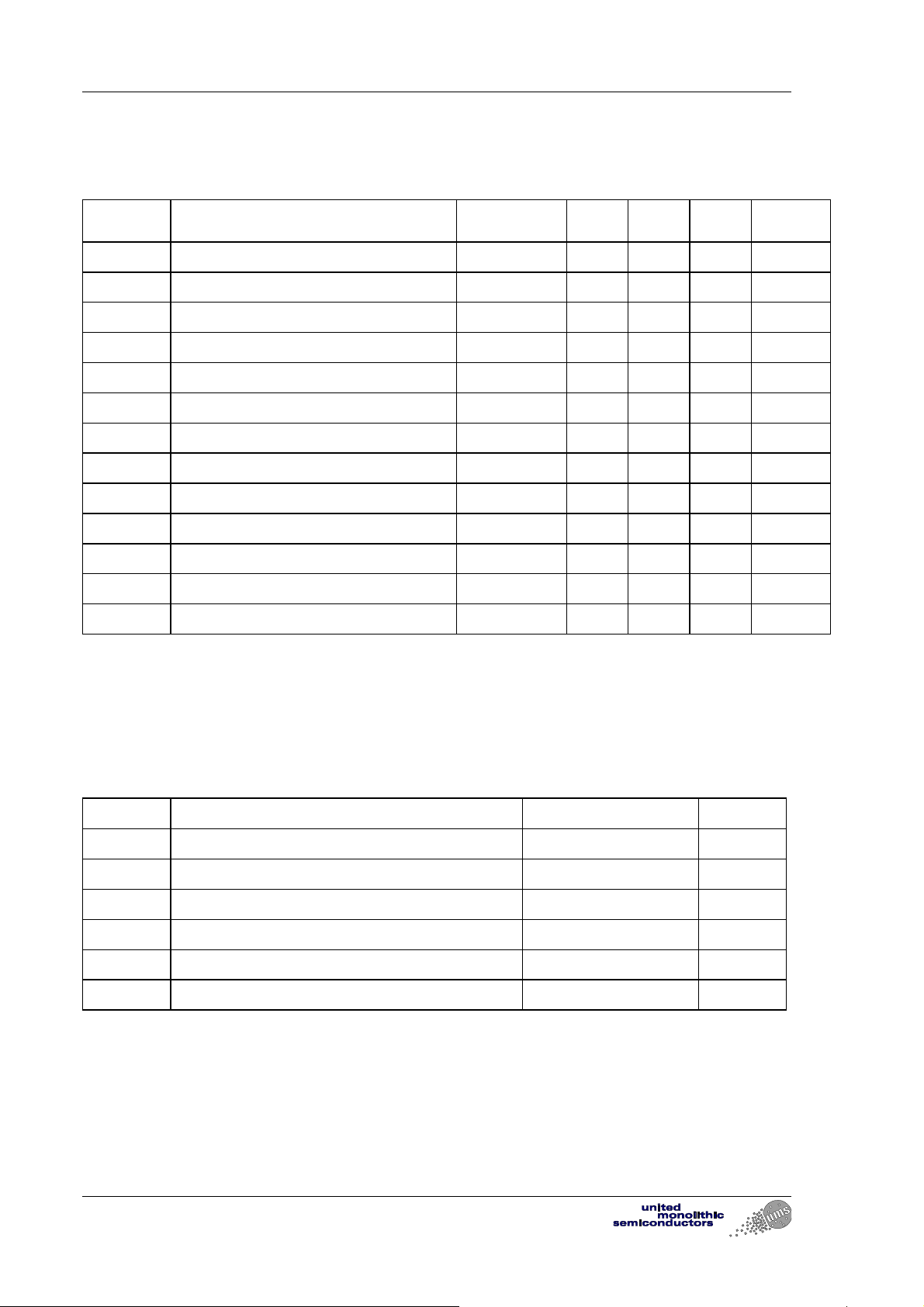
30
25
20
)
B
d
(
n
15
i
a
G
10
5
0
5 5,2 5,4 5,6 5,8 6 6,2 6,4 6,6 6,8 7
Frequency (GHz)
Main Characteristics
Tamb = +25°C
Symbol Parameter Min Typ Max Unit
Fop Operating freq uency range 5 5.8 7 GHz
Gmax Maximum gain 25 dB
∆G
Psat Saturated output power 27 dBm
ESD Protections : Electrostatic discharge sensitive device observe handling precautions !
Ref. : DSCHA52150160 -08-Jun-00 1/12 Specifications subject to change without notic e
Gain control range 10 15 dB
United Monolithic Semiconductors S.A.S.
Route Départementale 128 - B.P.46 - 91401 Orsay Cedex France
Tel. : +33 (0)1 69 33 03 08 - Fax : +33 (0)1 69 33 03 09
CHA5215a
Electrical Characteristics
Tamb = +25°C
5.8GHz Medium Power Amplifier
Symbol Parameter
Fop Operating freq uency range 5 5.8 7 GHz
Glin Linear gain ( Gc=-5V) 25 dB
Gdr Gain control dynamic range 10 15 dB
Gc Gain contro l voltage -5 0 V
Pout Saturated output power 27 dBm
Sdet Output power monitor sensitivity -5 mV/mW
Vref Reference monit or voltage 550 mV
RLin Input return loss (full band) (2) 7 12 dB
RLout Output return loss (2) 6 dB
Vd Positive supply voltage (1) 9 V
Id Positive supply current 330 400 mA
Vg Negative supply voltage -1.4 V
Ig Negative supply current 15 mA
(1) Depending on the application a trade-off can be obtained between linearity and power
consumption by adjusting the positive supply voltage (from 6 to 9V).
(2) The return loss can be improved by using a simple matching network (available on request).
Test
Conditions
Min. Typ. Max Unit
Absolute Maximum Ratings (1)
Tamb = +25°C
Symbol Parameter Values Unit
Vd Positive supply voltage 10 V
Vg Negat ive supply voltage -6 to 0 (3) V
Gc Gain control voltage -6 to 0.6
Pin Maximum peak input power overdrive (2) 20 dBm
Top Operating temperature range -50 to +70 °C
Tstg Storage temperature r ange -55 to +155 °C
(1) Operation of this device above anyone of these parameters may cause permanent damage
(2) Duration < 1s
(3) Choose Vg in order to have Id ≤ 400mA when Vd is applied
Ref. : DSCHA52150160 -08-Jun-00 2/12 Specifications subject to change without notic e
Route Départementale 128 , B.P.46 - 91401 ORSAY Cedex - FRANCE
Tel.: +33 (0)1 69 33 03 08 - Fax : +33 (0)1 69 33 03 09
5.8 GHz Medium Power Amplifier
Typical On Wafer Scattering Parameters
Bias Conditions : Vd = +5V Id=330mA (Vg = -1.4V) Gc = - 5V
CHA5215a
Freq.
GHz
4 -9.23 5.6 -47.73 162.4 0.33 -78.2 -8.28 105.5
4.1 -9.05 0.4 -48.42 142.3 2.86 -78.2 -7.72 90.6
4.2 -8.84 -5 -48.78 129.4 5.44 -89.7 --7.46 77.4
4.3 -8.65 -10.8 -50.4 113.1 7.93 -89.7 -7.22 -64.7
4.4 -8.44 -16.8 -50.72 101.3 10.36 -110.2 -6.96 52.6
4.5 -8.25 -23.2 -51.79 88.3 12.76 -110.2 -6.69 52.6
4.6 -8.07 -30.1 -51.93 73.9 15.1 -136.9 -6.38 -27.5
4.7 -7.93 -37.5 -52.56 59.8 17.38 -122.7 -6.1 13.8
4.8 -7.89 -45.4 -52.92 41.2 19.49 -171.3 -5.94 -0.17
4.9 -7.99 -53.7 -53.56 22.4 21.31 -153.1 -6.03 -15.9
5 -8.27 -61.5 -54.49 -0.2 22.75 146.5 -6.46 -30.7
5.1 -8.64 -68.7 -55.71 -22.4 23.74 168.2 -7.27 -44
5.2 -9.03 -74.9 -57.22 -45.7 24.35 102.9 -8.33 -54.2
5.3 -9.39 -80.9 -58.74 -69.8 24.69 124.4 -9.44 -61
5.4 -9.73 -86.6 -60.04 -93.3 24.83 63.8 -10.35 -64.5
5.5 -10.1 -92.4 -60.95 -119.4 24.88 82.7 -10.93 -66
5.6 -10.52 -97.9 -61.36 -144.1 24.86 29.1 -11.21 -66.8
5.7 -11 -103.1 -61.75 -168 24.77 46.1 -11.25 -67.8
5.8 -11.56 -107.6 -61.42 170.3 24.65 -2.4 -11.13 -68.9
5.9 -12.09 -11.1 -60.99 150.8 24.49 13 -10.98 -70.7
6 -12.62 -113.2 -60.57 134.4 24.33 -31 -10.74 -72.5
6.1 -13.05 -114.5 -60.34 117.6 24.19 -17.1 -10.54 -74.4
6.2 -13.21 -114.3 -59.89 105.9 24.09 -57.5 -10.35 -76.4
6.3 -13.14 -114.1 -59.38 93.5 24.03 -44.5 -10.15 -78.1
6.4 -12.77 -114.4 -58.47 82.1 23.98 -82.9 -9.92 -79.2
6.5 -12.18 -115.7 -57.61 70.1 24.02 -70.3 -9.63 -80.5
6.6 -11.48 -117.9 -56.81 59.1 24.09 -108.1 -9.27 -81.7
6.7 -10.65 -121.7 -55.59 44.2 24.2 -95.4 -8.79 -83.3
6.8 -9.76 -126.9 -55.19 31.3 24.37 -134.9 -8.35 -85.5
6.9 -8.9 -133.7 -54.39 17.7 24.52 -121.1 -7.86 -88.3
7 -8.03 -141.9 -53.67 0.7 24.65 -165.1 -7.4 -92
S11
dB
S11
////°
S12
dB
S12
////°
S21
dB
S21
////°
S22
dB
S22
////°
Ref. : DSCHA52150160 -08-Jun-00 3/ 12 Specifications subject to change without notic e
Route Départementale 128 , B.P.46 - 91401 ORSAY Cedex - FRANCE
Tel.: +33 (0)1 69 33 03 08 - Fax : +33 (0)1 69 33 03 09
CHA5215a
5.8GHz Medium Power Amplifier
Typical On Wafer Scattering Parameters
Bias Conditions : Vd = +5V Id=330mA (Vg = -1.4V) Gc = 0V
Freq.
GHz
4 -22.97 169.9 -34.74 25.6 -6.22 -172.9 -9.34 98.1
4.1 -22.15 159 -36.83 7.2 -4.74 -179.4 -8.85 84.5
4.2 -21.67 149.3 -39.2 -7.2 -3.27 172 -8.7 72.1
4.3 -21.35 141.2 -41.02 -21.2 -1.91 162.4 -8.55 60.6
4.4 -21.16 133.9 -42.96 -32.2 -0.62 152 -8.42 49.6
4.5 -21.03 127.4 -44.55 -44.2 0.63 141.2 -8.26 38.7
4.6 -20.94 121.3 -46.11 -54.2 1.84 129.6 -8.04 27.7
4.7 -21 115.9 -47.53 -66.2 3.01 117.4 -7.8 16.4
4.8 -21.08 110.6 -48.79 -77.7 4.12 104.3 -7.56 4.8
4.9 -21.27 106.4 -50.14 -91.6 5.13 90.4 -7.39 -7.3
5 -21.5 102.4 -51.39 -105.3 5.99 75.7 -7.32 -19.6
5.1 -21.8 99.6 -52.81 -121.3 6.67 60.5 -7.43 -31.8
5.2 -22.06 97.1 -54.39 -139.6 7.14 45.1 -7.74 -43.2
5.3 -22.27 95.6 -55.86 -158.3 7.42 30.1 -8.24 -53.6
5.4 -22.47 94.1 -57.39 -177.5 7.55 15.9 -8.88 -62.2
5.5 -22.59 92.9 -58.53 161.5 7.58 2.6 -9.62 -69
5.6 -22.69 91.6 -59.33 140.9 7.57 -10 -10.38 -73.8
5.7 -22.8 90.4 -59.48 119.9 7.58 -21.7 -11.1 -76.7
5.8 -22.9 89 -59.27 101.7 7.62 -32.9 -11.7 -77.5
5.9 -23.14 88 58.76 84.8 7.72 -43.7 -12.14 -76.8
6 -23.38 86.6 -58.03 68.8 7.91 -54.2 -12.31 -74.7
6.1 -23.7 86.9 -57.17 53.3 8.19 -64.9 -12.23 -72.2
6.2 -24.15 87 -56.52 39.9 8.56 -75.9 -11.83 -69.4
6.3 -24.62 89.3 -55.51 27.7 9.02 -87.5 -11.16 -67.3
6.4 -25.03 94.1 -54.47 16 9.55 -100.1 -10.23 -66.4
6.5 -25.04 102.4 -53.41 1 10.1 -114.2 -9.15 -67.5
6.6 -24.31 110.2 -52.5 -14.7 10.6 -129.9 -8.02 -70.8
6.7 -22.84 115.5 -51.5 -30.3 10.89 -147.6 -7.02 -76.5
6.8 -21.18 115.4 -51.21 -50.7 10.83 -166.8 -6.33 -84.2
6.9 -19.83 111 -51.51 -68.5 10.31 173.9 -6.06 -92.3
7 -18.99 105.2 -51.88 -84.2 9.39 155.9 -6.14 -99.7
S11
dB
S11
////°
S12
dB
S12
////°
S21
dB
S21
////°
S22
dB
S22
////°
Ref. : DSCHA52150160 -08-Jun-00 4/12 Specifications subject to change without notic e
Route Départementale 128 , B.P.46 - 91401 ORSAY Cedex - FRANCE
Tel.: +33 (0)1 69 33 03 08 - Fax : +33 (0)1 69 33 03 09
 Loading...