

United Monolithic Semiconductors CHA2190-99F-00 Datasheet
20-30GHz Low No ise Amplifier
self biased
GaAs Monolithic Microwave IC
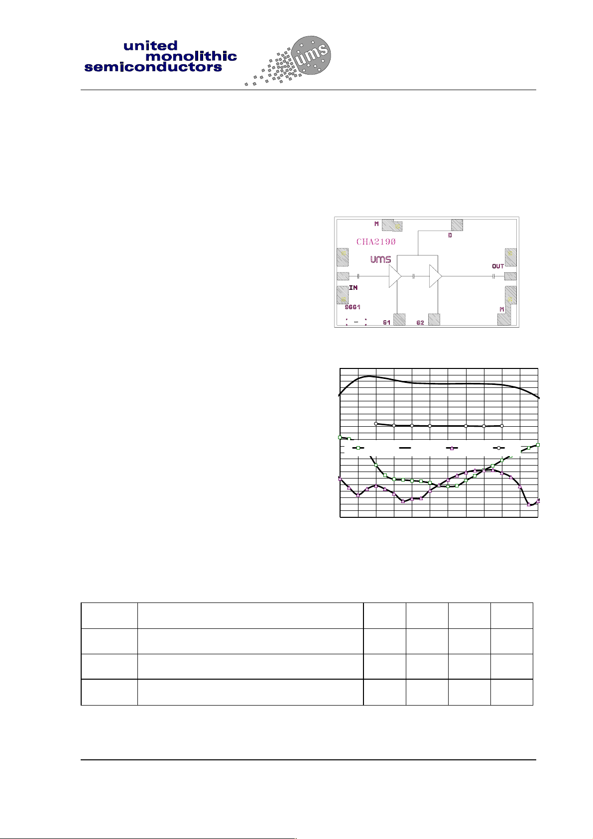
Description
The circuit is a two-stages self biased wide
band monolithic low noise amplifier.
The circuit is manufactured with a standard
HEMT process : 0.25µm gate length, via
holes through the substrate, air bridges and
electron beam gate lithogr aphy.
It is supplied in chip form.
Main Feature
§ Broad band performance 20-30GHz
§ 2.2dB noise figure
§ 15dB gain, ± 0.5dB gain f latness
§ Low DC power consumption, 50mA
§ 20dBm 3rd order intercept point
§ Chip size : 1.670 x 1.03x 0.1mm
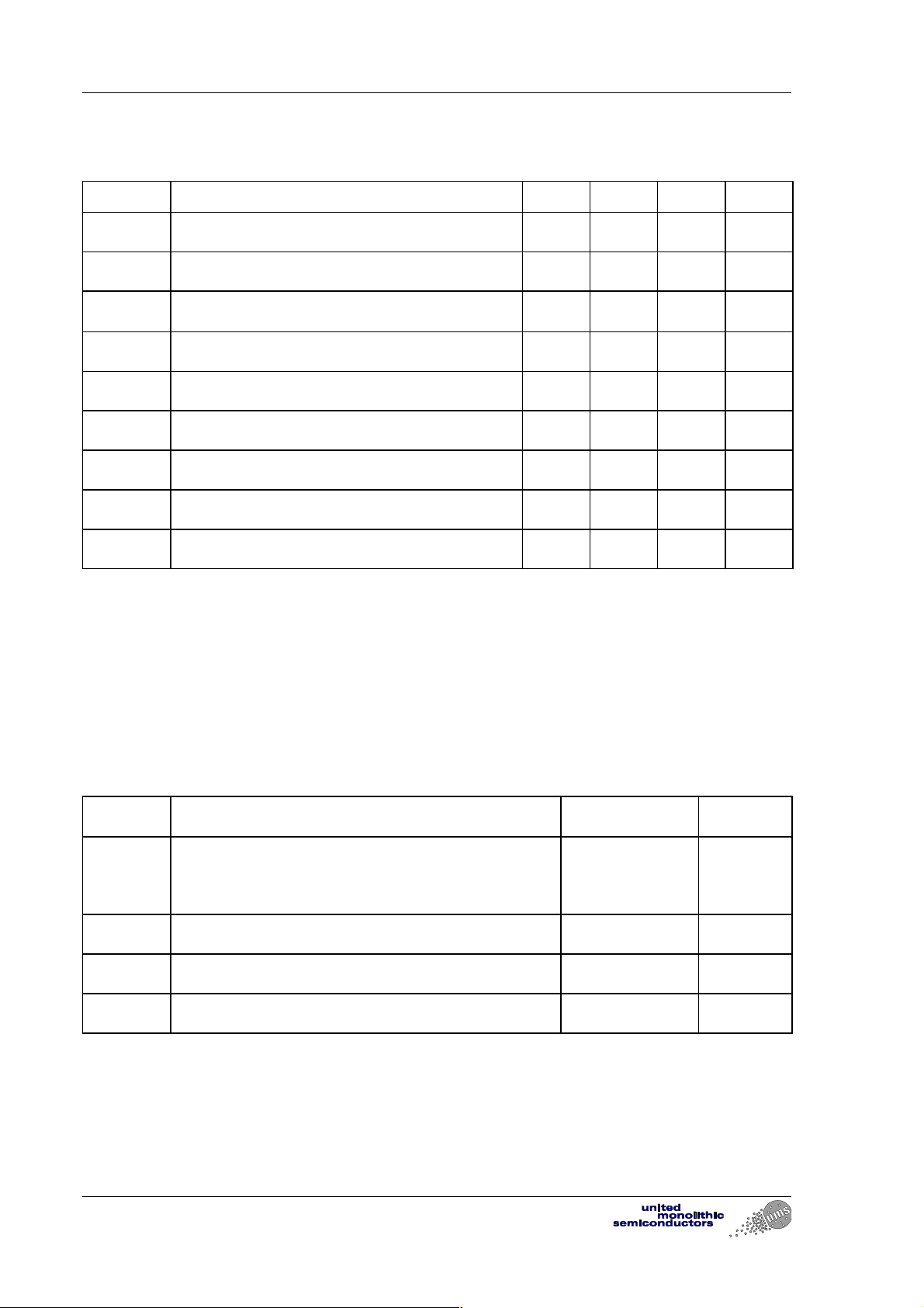
CHA2190
18
14
10
6
2
-2
-6
-10
dBSij & NF ( dB )
-14
-18
-22
-26
dBS11 dBS21 dBS22 NF
14 16 18 20 22 24 26 28 30 32 34 36
Frequency ( GHz )
Main Characteristics
Tamb = +25°C
Symbol Parameter Min Typ Max Unit
NF Noise figure at freq : 40GHz 2.2 3 dB
G Gain 13 15 dB
∆G
ESD Protections : Electrostatic discharge sensitive device observe handling precautions !
Ref : DSCHA21902036 -05-Feb.-02- 1/9 Specifications subject to change without notice
Gain flatness
United Monolithic Semiconductors S.A.S.
Route Départementale 128 - B.P.46 - 91401 Orsay Cedex France
Tel. : +33 (0)1 69 33 03 08 - Fax : +33 (0)1 69 33 03 09
On wafer typical measurement
± .0.5 ± 1
dB
CHA2190
20-30GHz Low Noise Amplifier
Electrical Characteristics
Tamb = +25°C, Vd = +4V (On wafer)
Symbol Parameter Min Typ Max Unit
Fop Operating freq uency range 20 30 Ghz
G Gain (1) 13 15 dB
∆G
Gain flatness (1)
NF Noise figure (1)
± 0.5 ± 1
2.2 3 dB
dB
VSWRin Input VSWR (1) 3.0:1
VSWRout Ouput VSW R (1) 3.0:1
IP3 3rd order intercept point 20 dBm
P1dB
Output power at 1dB gain compression (2)
11 dBm
Id Drain bias current (3) 50 70 mA
(1) These values are representative of wafer measurements without bonding wire at the RF ports.
(2)This value is a typical value when Vd=4V Vg1=Vg2=0V or not connected and can be increased
See chip biasing option page 8
(3) This current is the typical value for low noise and low current consumption biasing :
Vd=4V , Vg1=Vg2=0V or not connected.
Absolute Maximum Ratings (4)
Tamb = +25°C
Symbol Parameter Values Unit
Vd
Vg
Drain bias voltage (6)
Vg1 and Vg2 max
4.5
+1
V
V
Pin Maximum peak input power overdrive (5) 15 dBm
Top Operating tem per ature range -40 to +85 °C
Tstg Storage temperat ur e r ange -55 t o +125 °C
(4) Operation of this device above anyone of these paramaters may cause permanent damage.
(5) Duration < 1s.
(6) See chip biasing options page 8/9
Ref : DSCHA21902036 -05-Feb.-02- 2/9 Specifications subject to change without notic e
Route Départementale 128 , B.P.46 - 91401 ORSAY Cedex - FRANCE
Tel.: +33 (0)1 69 33 03 08 - Fax : +33 (0)1 69 33 03 09
20-30GHz Low Noise Amplifier
CHA2190
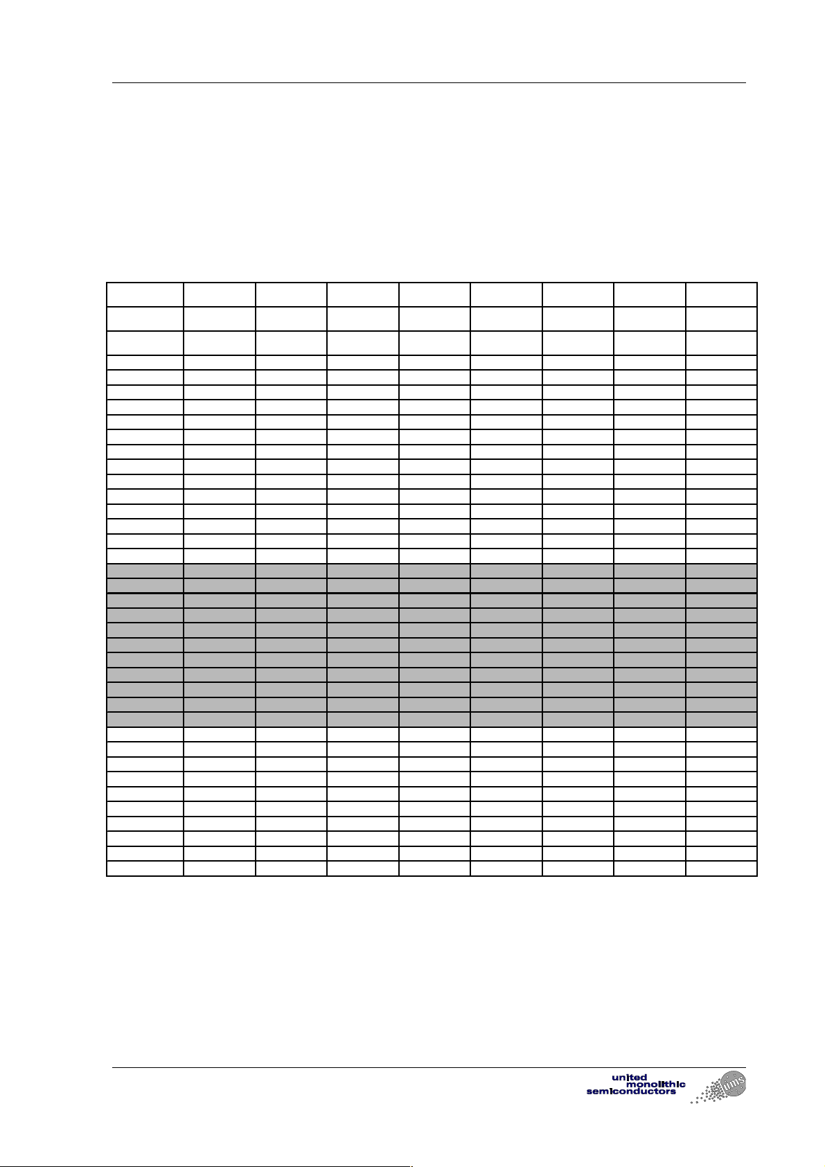
Typical Results
Chip Typical Response ( On wafer Scattering parameters ) :
Tamb = +25°C Vd=4V Id=+50mA
Freq dBS11 PS11 dBS12 PS12 dBS21 PS21 dBS22 PS22
mod. pha. mod. pha. mod. pha. mod. pha.
GHz dBdeg.dBdeg.dBdeg.dBdeg.
2.00 -0.37 -74.86 -70.84 -53.91 -29.15 56.50 -2.03 -84.36
5.00 -0.53 -151.19 -61.97 -91.19 -54.49 149.52 -4.15 -155.38
8.00 -0.59 157.19 -63.84 -162.71 -21.34 -178.25 -5.97 161.51
9.00 -0.66 141.20 -64.59 167.32 -14.41 176.87 -6.38 149.74
10.00 -0.79 125.32 -62.91 152.65 -7.52 163.27 -7.07 136.72
11.00 -1.00 109.39 -62.00 165.51 -1.20 140.92 -8.02 124.05
12.00 -1.26 93.11 -61.10 65.75 4.21 111.98 -9.38 111.29
13.00 -1.33 73.86 -54.13 -36.78 8.62 79.00 -11.25 101.00
14.00 -1.39 52.92 -45.84 -88.69 12.13 43.65 -14.06 92.70
15.00 -1.79 26.36 -41.70 -126.55 14.89 7.60 -16.84 90.96
16.00 -3.06 -7.27 -38.40 -159.80 16.82 -31.20 -19.09 106.80
17.00 -5.59 -46.11 -36.52 168.18 17.53 -68.31 -17.25 106.98
18.00 -9.90 -88.64 -34.29 139.94 17.39 -102.75 -16.27 97.39
19.00 -13.09 -132.63 -34.84 112.28 16.98 -131.32 -17.29 75.43
20.00 -14.29 -179.39 -34.82 93.31 16.44 -156.45 -18.70 49.82
21.00 -14.48 143.23 -34.24 79.42 15.90 -179.20 -21.00 23.10
22.00 -14.71 118.23 -33.88 62.77 15.50 160.71 -20.27 -12.66
23.00 -14.92 100.80 -33.65 47.72 15.38 141.01 -20.10 -51.60
24.00 -15.42 87.80 -32.93 34.93 15.30 121.05 -17.74 -76.68
25.00 -16.38 78.89 -32.22 20.45 15.22 101.34 -16.09 -98.65
26.00 -16.55 77.15 -31.63 3.26 15.22 81.83 -14.40 -114.01
27.00 -16.33 77.12 -30.73 -11.52 15.24 61.81 -13.10 -131.22
28.00 -14.66 71.74 -30.72 -31.79 15.28 41.14 -12.13 -145.23
29.00 -13.19 61.95 -29.96 -45.41 15.27 20.38 -11.55 -159.84
30.00 -11.49 46.38 -29.74 -65.11 15.22 -1.31 -11.52 -175.03
31.00 -10.10 25.97 -29.29 -84.32 15.13 -23.85 -11.39 171.38
32.00 -8.49 1.99 -29.08 -104.88 14.92 -47.58 -12.30 155.28
33.00 -7.01 -24.08 -29.25 -127.09 14.46 -72.54 -13.60 135.95
34.00 -5.76 -50.88 -28.83 -147.90 13.73 -98.45 -16.45 111.53
35.00 -4.56 -78.91 -29.98 -177.63 12.61 -124.59 -22.00 75.08
36.00 -3.67 -103.63 -31.24 165.34 11.09 -149.58 -20.99 -22.73
37.00 -3.02 -125.99 -31.84 144.11 9.30 -173.89 -17.26 -69.71
38.00 -2.57 -146.23 -35.07 127.07 7.29 163.92 -12.77 -88.90
39.00 -2.18 -162.01 -35.66 98.71 5.36 143.17 -10.42 -108.31
40.00 -1.82 -178.56 -36.87 109.75 3.19 121.75 -8.88 -119.32
Ref : DSCHA21902036 -05-Feb.-02- 3/9 Specifications subject to change without notice
Route Départementale 128 , B.P.46 - 91401 ORSAY Cedex - FRANCE
Tel.: +33 (0)1 69 33 03 08 - Fax : +33 (0)1 69 33 03 09
 Loading...