


查询UT912DL-S20-T供应商
UNISONIC TECHNOLOGIES CO.,
UT912D CMOS IC
DECODERS FOR REMOTE
CONTROLLER
DESCRIPTION
The UTC UT912D of CMOS LSIs for remote control system
applications are paired with UTC UT912E (refer to the
encoder/decoder cross reference table) and is capable of
decoding information which consists of N address bits and 12-N
data bits. For proper operation, a pair of encoder/decoder with the
same number of addresses and data format should be chosen.
The UTC UT912D also is arranged to provide 8 address bits and
4 data bits.
The decoders receive serial addresses and data from a
programmed UTC UT912E of encoders that are transmitted
together with the header bits by a RF or an infrared transmission
medium upon receipt of a trigger signal. If no error or unmatched
codes are found, the input data codes are decoded and then
transferred to the output pins. The V
indicate a valid transmission.
pin also goes high to
T
FEATURES
* Pair with UTC UT912E
* Operating voltage: 2.4V ~ 12V
* Low power and high noise immunity CMOS technology
* Low standby current
* Built-in oscillator needs only 5% resistor
* Binary address setting
* Received codes are checked 3 times
* Capable of decoding 12 bits of information
* Address/Data number combination: 8 address bits and 4 data
bits
* Vaild transmission indicator
* Minimal external components
SOP-20
DIP-18
*Pb-free plating product number: UT912DL
ORDERING INFORMATION
Order Number
Normal Lead free
Package Packing
UT912D-D18-T UT912DL-D18-T DIP-18 Tube
UT912D-S20-R UT912DL-S20-R SOP-20 Tape Reel
UT912D-S20-T UT912DL-S20-T SOP-20 Tube
ENCODER/DECORDER CROSS REFERENCE TABLE
Decoder Part No. Data Pins Address Pins VTPair Encoder
UTC UT912D
4 8 √
UTC UT912E
Encoder Decoder
DIP-14/18 SOP-16/20 DIP-18 SOP-20
Package
www.unisonic.com.tw 1
Copyright © 2005 Unisonic Technologies Co., QW-R502-044,A
UT912D CMOS IC
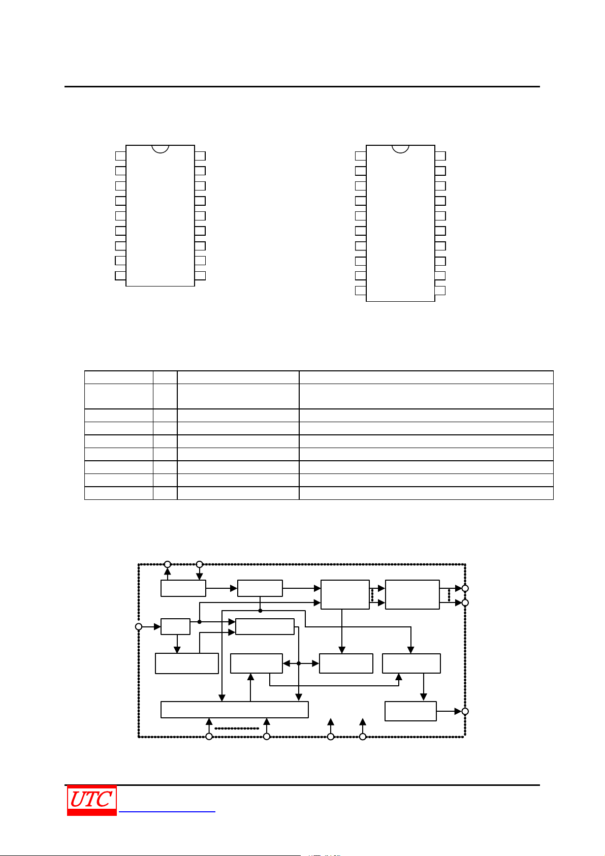
PIN CONFIGURATION
DIP-18
1
A0
2
A1
3
A2
4
A3
5
A4
6
A5
7
A6
8
A7
SS
V
9
18
16
15
14
13
12
11
10
17
V
DD
VT
OSC1
OSC2
DIN
D11
D10
D9
D8
V
NC
A0
A1
A2
A3
A4
A5
A6
A7
SS
SOP-20
1
2
3
4
5
6
7
8
9
10
PIN DESCRIPTION
PIN NAME I/O INTERNAL CONNECTION DESCRIPTION
A0 ~ A7 I NMOS Transmission Gate
D8 ~ D11 O CMOS OUT Output data pins, power-on state is low.
DIN I CMOS IN Serial data input pin
VT O CMOS OUT Valid transmission, active high
OSC1 I Oscillator Oscillator input pin
OSC2 O Oscillator Oscillator output pin
VSS Negative power supply, (GND)
VDD Positive power supply
Input pins for address A0 ~ A7 setting, these pins can be
externally set to V
or left open.
SS
20
19
18
17
16
15
14
13
12
11
NC
DD
V
V
T
OSC1
OSC2
DIN
D11
D10
D9
D8
BLOCK DIAGRAM
OSC 2 OSC1
Oscillator
DIN
Buffer
Sync . Detector
UNISONIC TECHNOLOGIES CO., LTD 2
www.unisonic.com.tw QW-R502-044,A
Divider
Data Detector
Comparator
Tr ansm issi on Gate Cir cuit
Address
Data Shift
Register
Comparator
DD
V
V
SS
Latch Circuit
Contr ol Logi c
Buffer
Data
V
T
UT912D CMOS IC
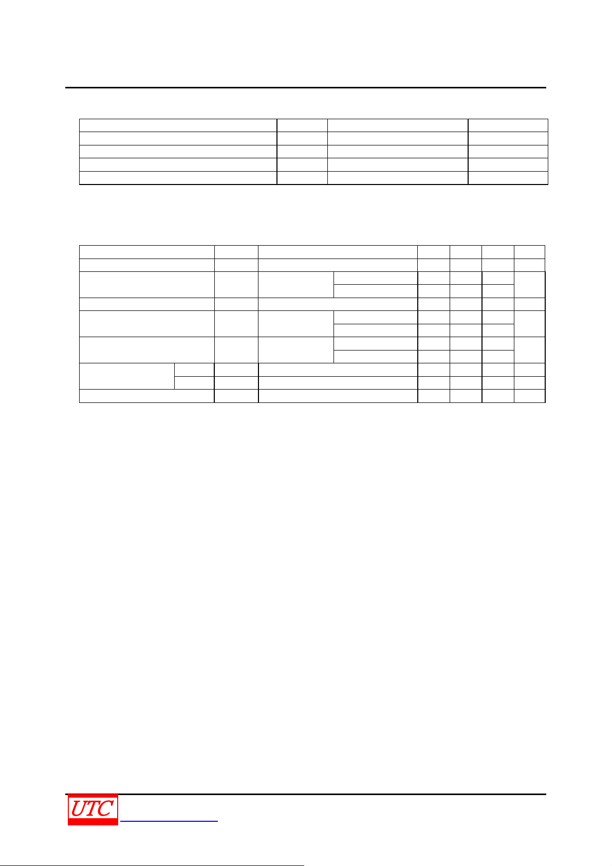
ABSOLUTE MAXIMUM RATINGS
PARAMETER SYMBOL RATINGS UNIT
Supply Voltage VDD -0.3 ~ +13 V
Input Voltage VIN Vss-0.3 ~ VDD+0.3 V
Operating Temperature T
Storage Temperature T
0 ~ +70
OPR
-40 ~ +150 ℃
STG
Note:Absolute maximum ratings are those values beyond which the device could be permanently damaged.
Absolute maximum ratings are stress ratings only and functional device operation is not implied.
ELECTRICAL CHARACTERISTICS (Ta=25℃, V
=5V, unless otherwise specified.)
DD
PARAMETER SYMBOL TEST CONDITIONS MIN TYP MAX UNIT
Operating Voltage V
Standby Current I
Operating Current I
Data Output Current (D8~D11) I
VT Output Current IVT VDD=5V
Input Voltage
High VIH 3.5 5 V
Low V
Oscillator Frequency f
2.4 5 12 V
OPR
Oscillator stops
STN-BY
No load, f
OPR
VDD=5V
DOUT
OSC
VDD=5V 0.1 1
VDD=12V 2 4
=150kHz, VDD=5V 159 400
VOH=4.5V (Source) -1 -1.99
V
=0.5V (Sink) 1 1.9
OL
VOH=4.5V (Source) -1 -1.564
V
=0.5V (Sink) 1 1.53
OL
0 1 V
IL
=1.1MΩ, VDD=5V
R
osc
osc
149 kHz
℃
μA
μA
mA
mA
UNISONIC TECHNOLOGIES CO., LTD 3
www.unisonic.com.tw QW-R502-044,A

UT912D CMOS IC
OPERATION FLOWCHART
The oscillator is disabled in the standby state and activated when a logic “high” signal applies to the DIN pin.
That is to say, the DIN should be kept low if there is no signal input.
Power
on
Standby
mode
No
No
Code in ?
Yes
Address bi ts
matched ?
Yes
Stor e data
Match
previous stor ed
data ?
Yes
3 times
of checking
com ple ted?
Yes
Disabl e VT&
ignore the r es t of
this word
No
No
Latch data
to output &
activate V
No
Address or
data er r or ?
T
Yes
UNISONIC TECHNOLOGIES CO., LTD 4
www.unisonic.com.tw QW-R502-044,A

UT912D CMOS IC
FUNCTIONAL DESCRIPTION
Operation
The UTC UT912D offers different packages by various combinations of addresses and data pins to pair with the
UTC UT912E. The decoders receive data that are transmitted by an encoder and interpret the first N bits of code
period as addresses and the last 12-N bits as data, where N is the address code number. A signal on the DIN pin
activates the oscillator, which in turn decodes the incoming address and data. The decoders will then check the
received address three times continuously. If the received address codes all match the contents of the decoder-s
local address, the 12-N bits of data are decoded to activate the output pins and the V
valid transmission. This will last unless the address code is incorrect or no signal is received. The output of the V
pin is high only when the transmission is valid. Otherwise it is always low.
Decoder timing
TE
pin is set high to indicate a
T
T
Encoder
DOUT
Decoder V
Latched
Data Out
T
< 1 word
4 words
check check
14
2 clocks
Tr ansmitted
Continuously
4 words
14
2 clock s
Address/Data sequence
The following provides the address/data sequence table for various models of the UTC UT912D. The correct
device should be selected according to the individual address and data requirements.
Bits 0 1 2 3 4 5 6 7 8 9 10 11
Address/
Data
A0 A1 A2 A3 A4 A5 A6 A7 D8 D9 D10 D11
UNISONIC TECHNOLOGIES CO., LTD 5
www.unisonic.com.tw QW-R502-044,A

UT912D CMOS IC
APPLICATION CIRCUITS
Recei v er C i r cuit
DD
1
A0
2
A1
3
A2
4
A3
5
A4
6
A5
7
A6
8
A7
9
SS
V
V
V
OSC1
OSC2
DIN
D11
D10
D9
D8
DD
T
APPROXIMATE INTERNAL CONNECTION CIRCUITS
18
17
16
15
14
13
12
11
10
V
Rosc
NMOS
Transmission Gate
CMOS OUT
CMOS IN
Oscillator
EN
OSC1
OSC2
UNISONIC TECHNOLOGIES CO., LTD 6
www.unisonic.com.tw QW-R502-044,A

UT912D CMOS IC
OSCILLATOR FREQUENCY VS SUPPLY VOLTAGE
fosc
(Scale)
Rosc (Ω )
4.00
3.50
27kΩ
3.00
2.50
2.00
1.50
(100kHz) 1.00
0.50
30kΩ
33kΩ
36kΩ
39kΩ
43kΩ
47kΩ
51kΩ
56kΩ
62kΩ
68kΩ
75kΩ
82kΩ
100kΩ
120kΩ
150kΩ
180kΩ
220kΩ
0.25
Note: The recommended oscillator frequency is f
2
3
456
OSCD
(decoder)≌50 f
7
91011
8
(UTC UT912E encoder)
OSCE
12 13
DD (VDC)
V
UTC assumes no responsibility for equipment failures that result from using products at values that
exceed, even momentarily, rated values (such as maxim um ratings, operating condition ranges, or
other parameters) listed in products specifications of any and all UTC products described or contained
herein. UTC products are not designed for use in life support appliances, dev ices or system s where
malfunction of these products can be reasonably expected to result in personal injury. Reproduction in
whole or in part is prohibited without the prior written consent of the copyright owner. The information
presented in this document does not form part of any quotation or contract, is believed to be accurate
and reliable and may be changed without notice.
UNISONIC TECHNOLOGIES CO., LTD 7
www.unisonic.com.tw QW-R502-044,A
 Loading...