


UTC UR0033 LINEAR INTEGRATED CIRCUIT
2 CHANNEL LOW-DROPOUT
VOLTAGE REGULATOR
FEATURES
*Dual Output: ADJ/1A, 3.3V/1A.
*Output Voltage Precision of ±2%.
*Output consists of PNP power transistor with
low-dropout voltage.
*Built-in over current protection circuit (OCP).
*Built-in Thermal Shut Down Circuit (TSD).
*Ideal for Hard Disk Drives applications.
1
TO-252-5
1: Vcc 2: ADJ 3: GND 4: Vo1 5: VO2
*Pb-free plating product number: UR0033L
PIN DISCRIPTION
PIN NO. PIN NAME FUNCTION
1 Vcc Power Supply
2 ADJ 1.25V
3 GND Ground
4 Vo1 ADJ Output
5 Vo2 3.3V Output
UTC UNISONIC TECHNOLOGIES CO., LTD. 1
QW-R102-023,A

UTC UR0033 LINEAR INTEGRATED CIRCUIT
BLOCK DIAGRAM
Vcc
PIN 1
Reference
Voltage
Thermal
Shut Down
Vcc
+
-
Current
Limit
Sat.
Prevention
Vcc
+
-
Current
Limit
Vcc
Vcc
Vo
PIN 4
ADJ
PIN 2
Vo2
PIN 5
1
Sat.
Prevention
PIN 3
GND
UTC UNISONIC TECHNOLOGIES CO., LTD. 2
QW-R102-023,A

UTC UR0033 LINEAR INTEGRATED CIRCUIT
ABSOLUTE MAXIMUM RATINGS (Ta=25℃)
PARAMETER SYMBOL RATINGS UNIT
Supply Voltage Vcc 18 V
Power dissipation PD 1000* mV
Operating temperature range Topr -40 ~ +85
Storage temperature range Tstg -55 ~ +150
Junction temperature Tj 150
* PD derated at 8mW/℃ for temperatures above Ta=25℃
OPERATING RATINGS
PARAMETER SYMBOL
Input Voltage Vcc 4.0 16.0 V
ADJ Output current Io1 1 A
3.3V Output current Io2 1 A
(Ta=25℃)
MIN MAX
ELECTRICAL CHARACTERISTICS
(Refer to the test circuit, Ta=25℃, VCC=6V unless otherwise specified.)
PARAMETER SYMBOL TEST CONDITIONS MIN TYP MAX UNIT
Bias Current IB Io1=0mA, Io2=0mA 0.8 1.5 mA
ADJ Output
Output Voltage 1 Vo1 Io1=500mA 1.225 1.25 1.275 V
Dropout Voltage 1
Peak Output Current 1 Io1 1.0 1.7 A
Ripple Rejection 1
Line Regulation 1
Load Regulation 1
Temperature Coefficient of Output
Voltage 1*
Short circuit Output Current 1 IOS1 Vcc=16V 270 mA
3.3V Output
Output Voltage 2 Vo2 Io2=500mA 3.234 3.30 3.366 V
Peak Output Current 2 Io2 1.0 1.7 A
Ripple Rejection 2
Line Regulation 2
Load Regulation 2
Temperature Coefficient of Output
Voltage 2*
Short circuit Output Current 2 IOS2 Vcc=16V 270 mA
* Design Guarantee. (Outgoing inspection is not done on all products.)
○ This product is not designed for protection against radioactive rays.
Note: All characteristic are measured with a capacity across the input (0.33μF) and the output (22μF).
Measurement is done at TA≒TJ, and variations in the parameter of all measurement (except for Temperature
Coefficient of Output Voltage)caused by temperature change are not considered.
△VD1
R.R.1
△VLINE1
△VLOAD1
TCVO1
R.R.2
△VLINE2
△V
LOAD2
TCVO2
Io1=500mA 0.25 0.5 V
f=120Hz, ein=1Vrms
Io1=200mA
Vcc=VO+1V ~ 16V,
Io1=500mA
Io1=0mA ~ 1A 30 75 mV
Io1=5mA, TJ=0 ~ 125℃
f=120Hz, ein=1Vrms
Io
2=200mA
Vcc=4V ~ 16V, Io1=500mA
2=0mA ~ 1A 30 75 mV
Io
Io
2=5mA, TJ=0 ~ 125℃
50 58 dB
5 30 mV
±0.01
50 58 dB
5 30 mV
±0.01
°C
°C
°C
UNIT
%/℃
%/℃
UTC UNISONIC TECHNOLOGIES CO., LTD. 3
QW-R102-023,A

UTC UR0033 LINEAR INTEGRATED CIRCUIT
POWER DISSIPATION
POWER DISSIPATION, PD (W)
12.5
10
7.5
2.5
5
0
0
(1) 10.0
(2) 1.0
(1) With infinitc Aluminum heat sink
θj-c=12.5 (℃/W)
(2) With no heat sink
θj-a=125.0( /W)℃
25 50 75 100 125 150
AMBIENT TEMPERATURE, T
STANDARD APPLICATION CIRCUIT
Vo1
Vcc
GND
Vo2
22μF
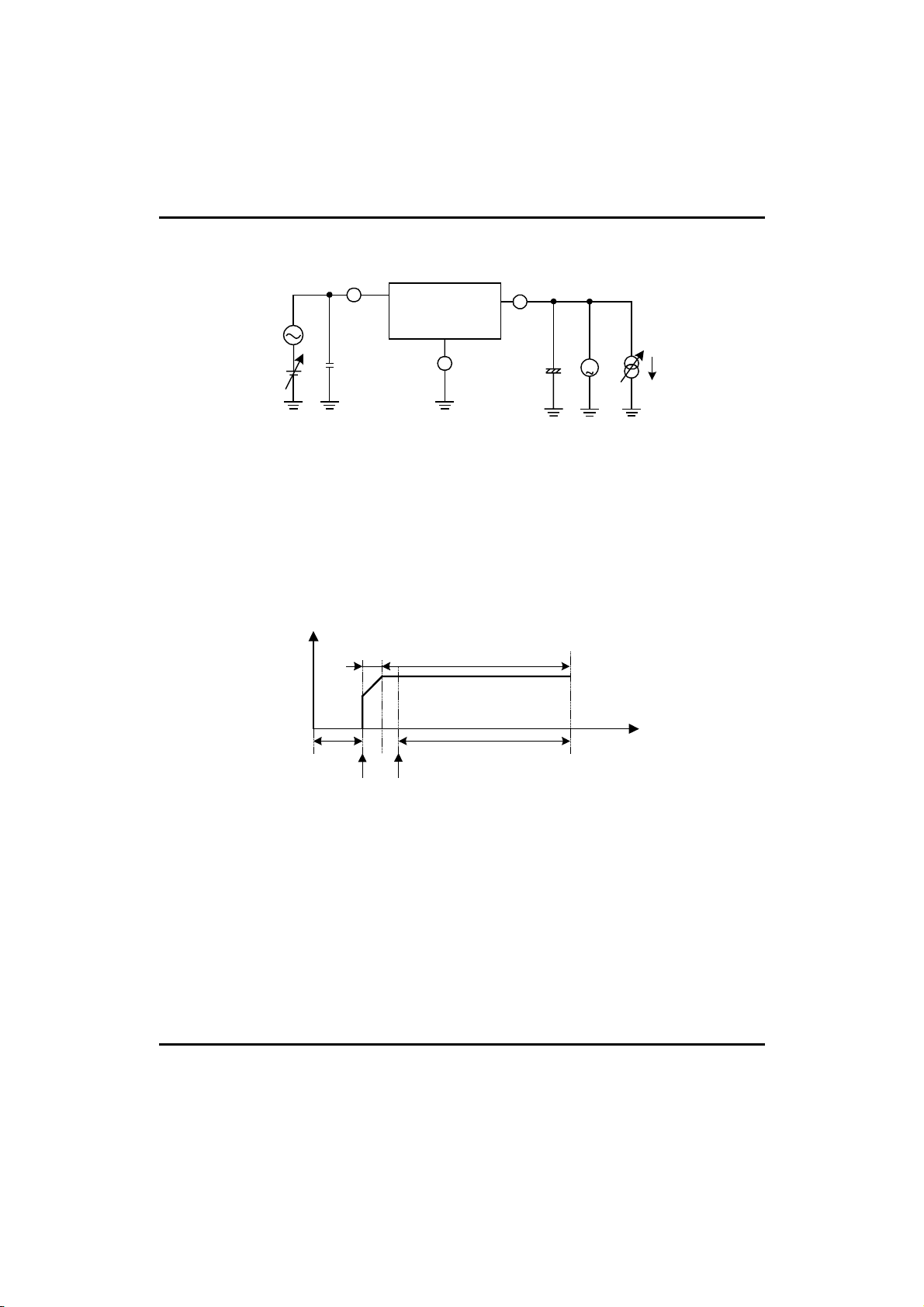
TEST CIRCUIT FOR EACH CONDITION
V
Vcc
GND
0.33μF
A
+
Vo1
or
Vo
2
OR
22μF
a (℃)
22μF
1Ω
10μF
Ceramic
+
+
OR
1Ω
10μF
Ceramic
A
Io
UTC UNISONIC TECHNOLOGIES CO., LTD. 4
QW-R102-023,A
UTC UR0033 LINEAR INTEGRATED CIRCUIT
TEST CIRCUIT FOR RIPPLE REJECTION RATIO
Vcc
ein
V
IN
0.33μF
GND
Vo1
or
Vo2
22μF
+
V
Io
APPLICATION INFORMATION
Operation Supply Voltage Range
The circuit functionality is guaranteed within operation of ambient temperature range, as long as it is within
operation supply voltage range. The standard electrical characteristic values are guaranteed at the test circuit
voltage of Vcc=VO+1V. The cannot be guaranteed at other voltages in the operating range of VO+1V ~ 16.0V,
homever, the variation will be small.
● Input /Output characteristic
V
OUT
Dropout Region
Off Region
Regulation Region
Recommended Operating Region
V
in
2V 3V
A=25℃)
(Typ.T
For proper regulation, this device must be operated in the Recommended Operating Region shown above.
Power Dissipation
Refer to the thermal duration characteristics shown in Fig.3. Also, be sure to use this IC within a power dissipation
rage allowing enough margins.
Output and Bypass Capacitor
To prevent oscillations, place the output capacitor between the output pin and GND for both channel. There is a
possibility for oscillation if capacitor's value changes due to temperature, voltage, etc. More than 22μF electrolytic
capacitor is recommended. If an extremely large value of (over 1000μF) is used, it may cause oscillations at low
frequency. In case of using ceramic capacitor (it is recommended more than 10μF) connect with 1Ω resistance
serially as ESR. For the bypass capacitor, a 0.33μF capacitor placed as close to Vcc pin and GND pin as possible
is recommended.
UTC UNISONIC TECHNOLOGIES CO., LTD. 5
QW-R102-023,A

UTC UR0033 LINEAR INTEGRATED CIRCUIT
Over- current Protection Circuit
The over-current protection circuits are built in at the outputs. They protect the IC from being damaged when the
load is short-circuited or subjected to an over current condition. This protection circuits perform holdback current
limiting.
Thermal Protection Circuit
A thermal shut down circuit (T.S.D.) is built into the IC to prevent damage due to overheating, Therefore, all the
outputs are turned off when the T.S.D. circuit is activated and are turned on when the temperature recedes to the
specified level. However, the T.S.D. circuit is only for extreme conditions and the regulator circuit should still be
designed for the IC not to exceed T
Grounding
It is recommended that every capacitor (bypass and output capacitors) is grounded to PIN3 using single-point
connections.
Electromagnetic Fields
The IC is susceptible to strong electromagnetic fields and may cause malfunction. Therefore, caution should be
used when placing it on the PCB.
Protection Diodes
It is recommended that protection diodes be used when the output is connected to an inductive load.
UTC assumes no responsibility for equipment failures that result from using products at values that
exceed, ev en momentarily, rated values (such as maximum ratings, operating condition ranges, or
other parameters) listed in products specifications of any and all UTC products described or contained
herein. UTC products are not designed for use in life support appliances, dev ices or systems where
malfunction of these products can be reasonably expected to result in personal injury. Reproduction in
whole or in part is prohibited without the prior written consent of the copyright owner. The information
presented in this document does not form part of any quotation or contract, is believed to be accurate
and reliable and may be changed without notice.
J(max)=150℃.
UTC UNISONIC TECHNOLOGIES CO., LTD. 6
QW-R102-023,A
 Loading...