

UNISONIC TECHNOLOGIES CO., LTD
U74LVC2G240
CMOS IC
DUAL BUFFER/DRIVER WITH
3-STATE OUTPUTS
DESCRIPTION
The U74LVC2G240 is a dual buffer or driver with 3-state
outputs. It is designed for 1.65V to 5.5V operation.
The U74LVC2G240 is composed of two 1-bit buffers/drivers
with separate output-enable (
data passes from A (input) to Y (output). When
outputs are in the high-impedance state.
To ensure the high-impedance state during power up or power
down, OE should be tied to VCC through a pull-up resistor, and
the minimum value of the resistor is determined by the
current-sinking capability of the driver.
The U74LVC2G240 is fully specified for partial-power-down
applications using I
and prevents damaging current backflow through the device
when it is powered down.
OFF
. The I
FEATURES
) inputs. When OE is low,
OE
is high, the
OE
circuitry disables the outputs
OFF
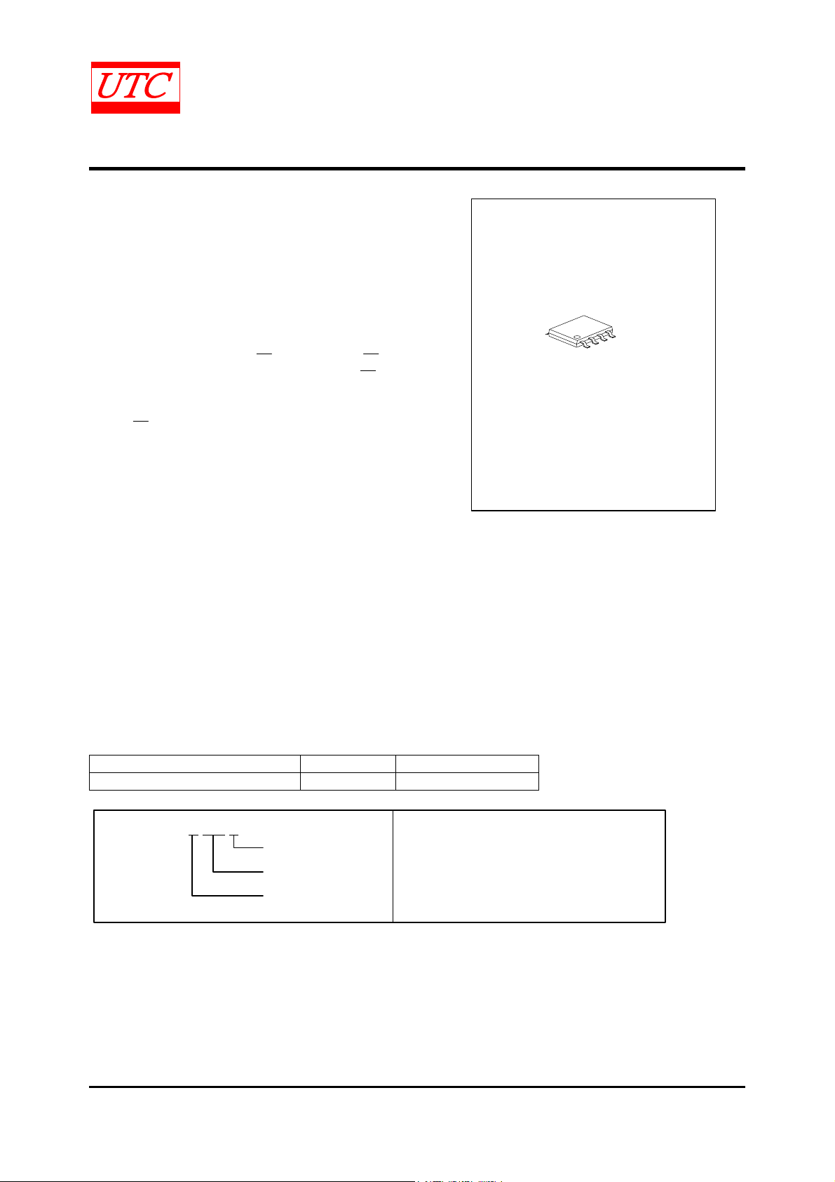
TSSOP-8
* Wide Supply Voltage Range from 1.65V to 5.5V
* Max t
* Up to 5.5V Inputs Accept Voltages
* Low Power Consumption, I
* ±24 mA Output Driver at 3.3V
* Typical V
V
* Typical V
V
of 4.6 ns at 3.3V
PD
(Output Ground Bounce) < 0.8V,
OLP
= 3.3 V, TA = 25 ℃
CC
(Output VOH Undershoot) > 2V,
OHV
= 3.3 V, T
CC
= 25 ℃
A
= 10 μA (Max.)
CC
ORDERING INFORMATION
Ordering Number Package Packing
U74LVC2G240G-P08-R TSSOP-8 Tape Reel
U74LVC2G240G-P08-R
(1) Packing Type
(2) Package Type
(3) Halogen Free
(1) R: Tape Reel
(2) P08:TSSOP-8
(3) G: Halogen Free
www.unisonic.com.tw 1 of 6
Copyright © 2010 Unisonic Technologies Co., Ltd QW-R502-433.A
U74LVC2G240 CMOS IC
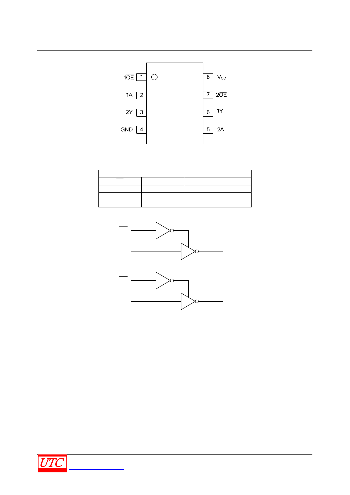
PIN CONFIGURATION
FUNCTION TABLE (Each Buffer)
INPUTS OUTPUT
OE
L H L
L L H
H X Z
LOGIC DIAGRAM (Positive Logic)
A Y
1
1OE
2
1A 1Y
7
2OE
5
2A 2Y
6
3
UNISONIC TECHNOLOGIES CO., LTD 2 of 6
www.unisonic.com.tw QW-R502-433.A

U74LVC2G240 CMOS IC
C
ABSOLUTE MAXIMUM RATING
PARAMETER SYMBOL RATINGS UNIT
Supply Voltage VCC -0.5~6.5 V
Input Voltage VIN -0.5~6.5 V
Output Voltage
(any output in the high-impedance or power-off state)
Output Voltage
(any output in the high or low state)
Input Clamp Current IIK -50 mA
Output Clamp Current IOK -50 mA
Output Current I
VCC or GND Current ICC ±100 mA
Storage Temperature T
Note: 1. The input and output voltage ratings may be exceeded if the input and output current ratings are observed.
2. Absolute maximum ratings are those values beyond which the device could be permanently damaged.
Absolute maximum ratings are stress ratings only and functional device operation is not implied.
THERMAL DATA
PARAMETER SYMBOL RATINGS UNIT
Junction to Ambient
RECOMMENDED OPERATING CONDITIONS
V
-0.5~6.5 V
OUT
V
-0.5~VCC+0.5 V
OUT
±50 mA
OUT
-65 ~ +150 °C
STG
θ
JA
190
°C /W
PARAMETER SYMBOL CONDITIONS MIN TYP MAX UNIT
Supply Voltage VCC
High-Level Input Voltage VIH
Low-Level Input Voltage VIL
Operating 1.65 5.5
Data retention only 1.5
VCC = 1.65V to 1.95V
0.65* VCC
VCC = 2.3V to 2.7V 1.7
VCC = 3V to 3.6V 2
V
= 4.5V to 5.5V
CC
0.7* VCC
VCC = 1.65V to 1.95V
0.35* V
VCC = 2.3V to 2.7V 0.7
VCC = 3V to 3.6V 0.8
V
= 4.5V to 5.5V
CC
0.3* V
V
V
C
V
CC
Input Voltage VIN 0 5.5 V
Output Voltage V
OUT
High or low state 0 VCC
3-state 0 5.5
V
VCC=1.65V -4
VCC=2.3V -8
High-Level Output Current IOH
VCC=3V
=4.5V -32
V
CC
-16
-24
mA
VCC=1.65V 4
VCC=2.3V 8
Low-Level Output Current IOL
Input Transition Rise or Fall Rate tR / tF
Operating Temperature T
OPR
VCC=3V
=4.5V 32
V
CC
16
24
VCC=1.8±0.15V, 2.5±0.2V 20
VCC=3.3±0.3V 10
VCC=5.0+0.5V 5
-40 85 °C
mA
ns/
V
UNISONIC TECHNOLOGIES CO., LTD 3 of 6
www.unisonic.com.tw QW-R502-433.A
U74LVC2G240 CMOS IC
A
ELECTRICAL CHARACTERISTICS (T
=25°C , V
A
= 3.3 V, unless otherwise specified)
CC
PARAMETER SYMBOL TEST CONDITIONS MIN TYP MAX UNIT
I
= -100 μAVCC = 1.65V to 5.5V VCC -0.1
OH
I
= -4 mA VCC = 1.65V 1.2
OH
I
= -8 mA VCC = 2.3V 1.9
High-Level Output Voltage VOH
Low-Level Output Voltage VOL
Input Leakage Current
(A or
OE
inputs)
OFF-State Current I
I
I(LEAK)
OFF
OH
I
OH
I
OH
I
OH
I
OL
I
OL
I
OL
I
OL
I
OL
I
= 32 mA VCC = 4.5V 0.55
OL
V
IN
V
IN
= -16 mA VCC = 3V 2.4
V
= -24 mA VCC = 3V 2.3
= -32 mA VCC = 4.5V 3.8
= 100 μAVCC = 1.65V to 5.5V 0.1
= 4 mA VCC = 1.65V 0.45
= 8 mA VCC = 2.3V 0.3
= 16 mA VCC = 3V 0.4
V
= 24 mA VCC = 3V 0.55
= 5.5V or GND, VCC = 0 to 5.5V ±5 μA
or VO = 5.5V, VCC = 0V ±10 μA
High-Impedance State Current IOZ VO = 0 to 5.5V, VCC = 3.6V 10 μA
V
= 5.5V or GND, I
Quiescent Supply Current IQ
dditional quiescent Supply
Current
Δ I
Input Capacitance CIN V
Output Capacitance C
OUT
IN
V
= 1.65V to 5.5V
CC
One input at V
other inputs at V
Q
V
=3V to 5.5V
CC
= VCC or GND, VCC=3.3V 4 pF
IN
V
OUT
CC
= VCC or GND, VCC=3.3V 6 pF
OUT
– 0.6V;
or GND;
CC
= 0,
10 μA
500 μA
SWITCHING CHARACTERISTICS (T
PARAMETER SYMBOL TEST CONDITIONS MIN TYP MAX UNIT
VCC=1.8±0.15V, RL=1KΩ 2 11.3
VCC=2.5±0.2V, RL=500Ω
t
/ t
PLH
(tPD)
PHL
VCC=3.3±0.3V,
R
=500Ω
L
V
CC
R
=500Ω
L
Propagation Delay
from Input A to Output Y
VCC=1.8±0.15V, RL=1KΩ 2.7 11.7
/ t
Propagation Delay
from Input
to Output Y
OE
t
PZL
(tEN)
PZH
VCC=2.5±0.2V, RL=500Ω
VCC=3.3±0.3V 1.4 5.4
V
CC
VCC=1.8±0.15V, RL=1KΩ 1.7 12.8
/ t
Propagation Delay
from Input
to Output Y
OE
t
PLZ
PHZ
VCC=2.5±0.2V, RL=500Ω
(t
)
VCC=3.3±0.3V 1.2 5.5
DIS
V
CC
OPERATING CHARACTERISTICS (T
PARAMETER SYMBOL TEST CONDITIONS MIN TYP MAX UNIT
Outputs enabled
Power Dissipation Capacitance per
buffer/driver
C
PD
Outputs disabled
=25°C)
A
=5±0.5V,
=5±0.5V
=5±0.5V
=25°C)
A
C
=30pF
L
1.4 5.5
1.1 4.6
=500Ω CL=50pF
R
L
1 4
=30pF
C
L
R
=500Ω CL=50pF
L
C
=30pF
L
RL=500Ω CL=50pF
1.9 6.6
1.1 5
0.8 5.7
0.5 4.2
VCC = 1.8V
VCC = 2.5V
VCC = 3.3V 15
V
= 5V
CC
f=10MHz
17
VCC = 1.8V 1
VCC = 2.5V 1
VCC = 3.3V 2
V
= 5V
CC
f=10MHz
2
ns
ns
ns
pF
pF
UNISONIC TECHNOLOGIES CO., LTD 4 of 6
www.unisonic.com.tw QW-R502-433.A
U74LVC2G240 CMOS IC
TEST CIRCUIT AND WAVEFORMS
TEST S1
t
t
t
VCC
INPUTS
t
V
IN
R
, tF
1.8V±0.15V VCC ≤2ns VCC/2 2*VCC 30pF 1KΩ 0.15V
2.5V±0.2V VCC ≤2ns VCC/2 2*VCC 30pF 500Ω 0.15V
3.3V±0.3V 3V ≤2.5ns 1.5V 6V 50pF 500Ω 0.3V
5V±0.5V VCC ≤2.5ns VCC/2 2*VCC 50pF 500Ω 0.3V
V
V
M
LOAD
C
Open
PLH/tPHL
V
PLZ/tPZL
GND
PHZ/tPZH
R
L
L
LOAD
V
Δ
Notes: 1. C
includes probe and jig capacitance.
L
2. All input pulses are supplied by generators having the following characteristics: PRR ≤10MHz, Z
= 50Ω.
O
UNISONIC TECHNOLOGIES CO., LTD 5 of 6
www.unisonic.com.tw QW-R502-433.A

U74LVC2G240 CMOS IC
UTC assumes no responsibility for equipment failures that result from using products at values that
exceed, even momentarily, rated values (such as maximum ratings, operating condition ranges, or
other parameters) listed in products specifications of any and all UTC products described or contained
herein. UTC products are not designed for use in life support appliances, devices or systems where
malfunction of these products can be reasonably expected to result in personal injury. Reproduction in
whole or in part is prohibited without the prior written consent of the copyright owner. The information
presented in this document does not form part of any quotation or contract, is believed to be accurate
and reliable and may be changed without notice.
UNISONIC TECHNOLOGIES CO., LTD 6 of 6
www.unisonic.com.tw QW-R502-433.A
 Loading...