

UNISONIC TECHNOLOGIES CO., LTD
U74HC2G32
2-INPUT OR GATE
DESCRIPTION
The U74HC2G32 is a 2-input OR gate which provides the
Function Y=A+B.
FEATURES
* Operation Voltage Range: 2.0~6.0V
* Low Power Dissipation: I
* High Speed: tpd=9ns(Vcc=4.5V, C
*Specified from -40 to +85℃ and -40 to +125℃
=10µA(Max)
CC
=50pF)
L
CMOS IC
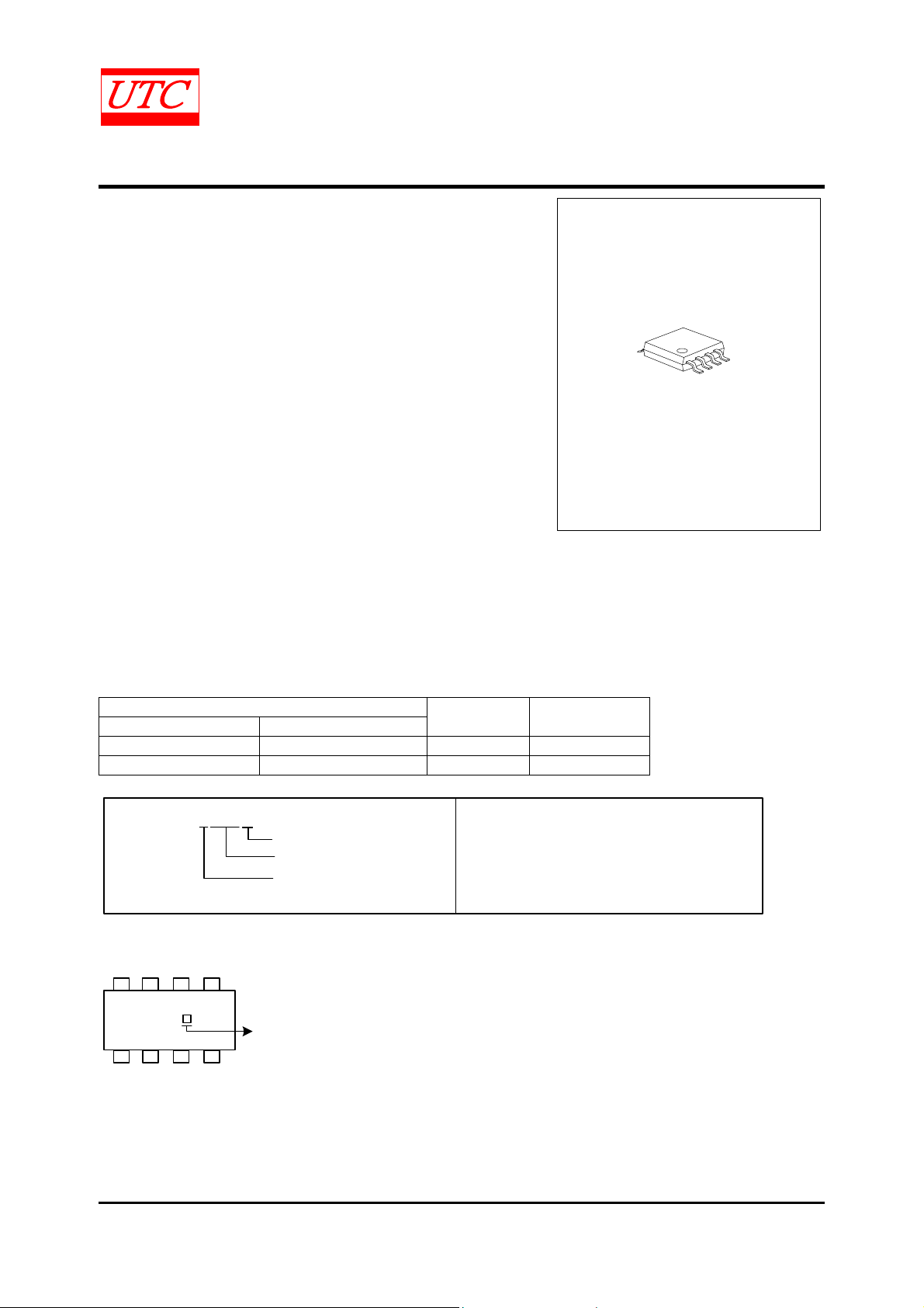
MSOP-8
*Pb-free plating product number:
U74HC2G32L
ORDERING INFORMATION
Order Number
Normal Lead Free Plating
U74HC2G32-SM1-R U74HC2G32L-SM1-R MSOP-8 Tape Reel
U74HC2G32-SM1-T U74HC2G32L-SM1-T MSOP-8 Tube
U74HC2G32L-SM1-R
(1)Packing Type
(2)Package Type
(3)Lead Plating
MARKING
Package Packing
(1) R: Tape Reel, T: Tube
(2) SM1: MSOP-8
(3) L: Lead Free Plating, Blank: Pb/Sn
5678
03B
4321
Lead Plating
www.unisonic.com.tw
Copyright © 2005 Unisonic Technologies Co., Ltd
1 of 5
QW-R502-083,A
U74HC2G32
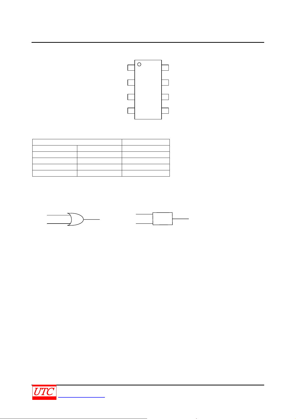
PIN CONFIGURATION
CMOS IC
FUNCTION TABLE
INPUT OUTPUT
A B Y
L L L
L H H
H L H
H H H
LOGIC DIAGRAM
A
B
1
7
2
(each gate)
(positive logic)
Y
1A
1B
2Y
GND
1
2
3
4
8
VCC
7
1Y
6
2B
2A
5
A
B
1
7
≥
2
Y
UNISONIC TECHNOLOGIES CO., LTD
www.unisonic.com.tw
2 of 5
QW-R502-083,A

U74HC2G32
CMOS IC
ABSOLUTE MAXIMUM RATING
(unless otherwise specified)(Note 1)
PARAMETER SYMBOL RATINGS UNIT
Supply Voltage VCC -0.5~7 V
Input Voltage VIN -0.5~7 V
Output Voltage V
-0.5~VCC+0.5 V
OUT
Input Clamp Current IIK ±20 mA
Output Clamp Current IOK ±20 mA
Output Current I
25 mA
OUT
VCC or GND Current ICC 50 mA
Power Dissipation PD 300 mW
Storage Temperature T
-65 ~ +150 ℃
STG
Note 1. The input and output voltage ratings may be exceeded if the input and output current ratings are observed.
2. Absolute maximum ratings are those values beyond which the device could be permanently damaged.
Absolute maximum ratings are stress ratings only and functional device operation is not implied.
RECOMMENDED OPERATING COMDITIONS
PARAMETER SYMBOL CONDITIONS MIN TYP MAX UNIT
Supply Voltage VCC 2.0 5.0 6.0 V
Input Voltage VIN 0 VCC V
Output Voltage V
Input Transition Rise or Fall Times tR ,tF
Operating Temperature TA -40 25 125
0 VCC V
OUT
VCC=2.0V 1000
VCC=4.5V 6 500
VCC=6V 400
ns
℃
STATIC CHARACTERISTICS
PARAMETER SYMBOL TEST CONDITIONS
VCC=2.0V 1.5 1.2 1.5 1.5
High-Level Input Voltage VIH
Low-Level Input Voltage VIL
High-Level Output
Voltage
Low-Level Output
Voltage
Input Leakage Current I
V
V
I(LEAK)
Quiescent Supply
Current
Input Capacitance CIN
VCC=4.5V
V
=6.0V
CC
VCC=2.0V
VCC=4.5V
V
=6.0V
CC
VCC=2.0V, IOH=-20µA 1.9 2.0 1.9 1.9
VCC=4.5V, IOH=-20µA 4.4 4.5 4.4 4.4
VCC=6.0V, IOH=-20µA 5.9 6.0 5.9 5.9
OH
VCC=4.5V, IOH=-4mA 4.18 4.32 4.13 3.7
V
=6.0V,
CC
I
=-5.2mA
OH
VCC=2.0V, IOL=20µA 0 0.1 0.1 0.1
VCC=4.5V, IOL=20µA 0 0.1 0.1 0.1
VCC=6.0V, IOL=20µA 0 0.1 0.1 0.1
OL
VCC=4.5V, IOH=4mA 0.15 0.26 0.33 0.4
V
=6.0V, IOH=5.2mA 0.16 0.26 0.33 0.4
CC
V
=6.0V, VIN=VCCor
CC
GND
V
=6.0V, VIN=VCCor
I
Q
CC
GND, I
OUT
V
=5.0V, VIN=V
CC
GND
=0
T
=25℃ -40~85℃ -40~125℃
A
MIN TYP MAX MIN MAX MIN MAX
3.15 2.4 3.15 3.15
4.2 3.2 4.2 4.2
0.8 0.5 0.5 0.5
2.1 1.35 1.35 1.35
2.8 1.8 1.8 1.8
5.68 5.81 5.63 5.2
±0.1 ±1 ±1 µA
1 10 20 µA
or
CC
1.5 pF
UNIT
V
V
V
V
UNISONIC TECHNOLOGIES CO., LTD
www.unisonic.com.tw
3 of 5
QW-R502-083,A

U74HC2G32
CMOS IC
DYNAMIC CHARACTERISTICS
See Fig-1 and Fig-2 for test circuit and waveforms.
PARAMETER SYMBOL TEST CONDITIONS
Propagation Delay From
Input (A and B) to
Output(Y)
Output Transition Time t
Operating Characteristics
PARAMETER SYMBOL TEST CONDITIONS TYP UNIT
Power Dissipation Capacitance Cpd No load, f=1MHz, VCC=5 10 pF
t
PHL
THL
VCC= 2.0, CL= 50pF 24 75 95 110
/t
VCC= 4.5, CL= 50pF 9 15 19 22
PLH
V
= 6.0, CL= 50pF 7 13 16 20
CC
VCC= 2.0, CL= 50pF 18 75 95 125
/t
VCC= 4.5, CL= 50pF 6 15 19 25
TLH
= 6.0, CL= 50pF 5 13 16 20
V
CC
(Input: tR,tF≤6ns;PRR≤1MHz)
T
=25℃ -40~85℃ -40~125℃
A
MIN TYP MAX MIN MAX MIN MAX
UNIT
ns
ns
UNISONIC TECHNOLOGIES CO., LTD
www.unisonic.com.tw
4 of 5
QW-R502-083,A

U74HC2G32
TEST CIRCUIT AND WAVEFORMS
Outp ut
C
L
(Note)
CMOS IC
Note: C
Input
Output
L
includes probe and jig capacitance.
Fig.1 Load circuitry for switching times.
1/2 * V
CC
t
PLH
90%
CC
1/2 * V
10%
t
TLH
Fig. 2 Propagation delay from input(A and B) to output(Y) and Output transition time.
1/2 * V
CC
90%
t
PHL
10%
t
THL
1/2 * V
CC
UTC assumes no responsibility for equipment failures that result from using products at values that
exceed, even momentarily, rated values (such as maximum ratings, operating condition ranges, or
other parameters) listed in products specifications of any and all UTC products described or contained
herein. UTC products are not designed for use in life support appliances, devices or systems where
malfunction of these products can be reasonably expected to result in personal injury. Reproduction in
whole or in part is prohibited without the prior written consent of the copyright owner. The information
presented in this document does not form part of any quotation or contract, is believed to be accurate
and reliable and may be changed without notice.
UNISONIC TECHNOLOGIES CO., LTD
www.unisonic.com.tw
QW-R502-083,A
5 of 5
 Loading...