

查询TL594L-D16-T供应商
UNISONIC TECHNOLOGIES CO., LTD
TL594
LINEAR INTEGRATED CIRCUIT
PULSE-WIDTH-MODULATION
CONTROL CIRCUIT
DESCRIPTION
The UTC TL594 incorporates all the functions required for a
pulse-width-modulation (PWM) control circuit. It is pin compatible
with TL494 with upgrade performance.
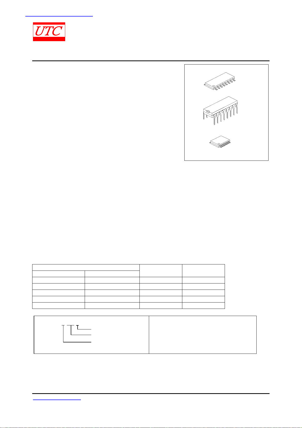
SOP-16
DIP-16
TSSOP-16
*Pb-free plating product number: TL594L
FEATURES
* Outputs for 200-mA Sink or Source
Current
* Output is Single-Ended or Push-Pull
Operation Selectable suppression circuit
* Internal Circuitry Prohibits Double Pulse
at Either Output
* Variable Dead Time
* Internal Reference Supply Deliuer 5V
within 1% tolerance
* Undervoltage Lockout for Low-V
Conditions
CC
ORDERING INFORMATION
Order Number
Normal Lead Free Plating
TL594-D16-T TL594L-D16-T DIP-16 Tube
TL594-P16-R TL594L-P16-R TSSOP-16 Tape Reel
TL594-P16-T TL594L-P16-T TSSOP-16 Tube
TL594-S16-R TL594L-S16-R SOP-16 Tape Reel
TL594-S16-T TL594L-S16-T SOP-16 Tube
TL594L-D16-T
(1)Packing Type
(2)Package Type
(3)Lead Plating
www.unisonic.com.tw 1 of 8
Copyright © 2005 Unisonic Technologies Co., Ltd QW-R103-031,A
Package Packing
(1) R: Tape Reel, T: Tube
(2) D16: DIP-16, S16: SOP-16, P16: TSSOP-16
(3) L: Lead Free Plating, Blank: Pb/Sn
TL594 LINEAR INTEGRATED CIRCUIT
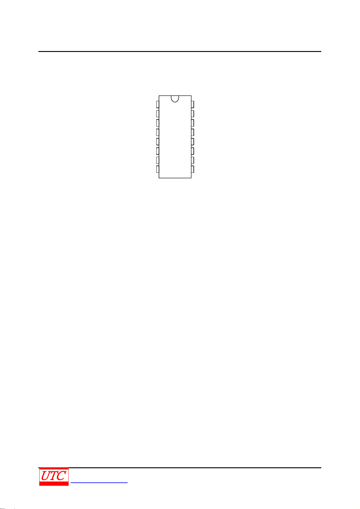
PIN CONFIGURATION
DIP-16/SOP-16/TSSOP-16 PACKAGE
(TOP VIEW)
16
1IN+
1IN
FEEDBACK
DTC
CT
RT
GND
C1
1
2
3
4
5
6
7
8
2IN+
15
2IN-
14
REF
13
Output CTRL
12
V
11
C2
10
E2
9
E1
CC
UNISONIC TECHNOLOGIES CO., LTD 2 of 8
www.unisonic.com.tw QW-R103-031,A
TL594 LINEAR INTEGRATED CIRCUIT
FUNCTIONAL BLOCK DIAGRAM
Deadtime
Comparator
+
-
-
+
PWM
Comparator
0.7mA
3
Feedback PWM
Comparator Input
CK Q
Flip–Flop
DQ
Reference
Regulator
12
V
CC
7
Gnd
IN+
IN-
IN+
IN-
Deadtime
Control
C
R
Error Amp 1
1
2
16
15
Error Amp 2
4
0.1V
T
Oscillator
T
0.7V
+
1
-
+
2
-
Output Co ntrol
14
Ref.
Outp ut
13
Lockout
UV
Q1
Q2
11
10
C2
E2
8
C1
9
E1
UNISONIC TECHNOLOGIES CO., LTD 3 of 8
www.unisonic.com.tw QW-R103-031,A

TL594 LINEAR INTEGRATED CIRCUIT
ABSOLUTE MAXIMUM RATINGS
(over operating free-air temperature range (unless otherwise noted)
PARAMETER SYMBOL RATINGS UNIT
Supply Voltage V
Amplifier input voltage VCC + 0.3 V
Collector output voltage 41 V
Collector output current 250 mA
Operating Junction Temperature TJ +150 °C
Operating Free-Air Temperature TA -40 ~ +85 °C
Storage Temperature T
Note 1. Stresses beyond “absolute maximum ratings” may cause permanent damage to the device. For reliability,
considerations use 80% or below for application is recommended.
Note1
)
CC
-40 ~ 150 °C
STG
41 V
THERMAL DATA
PARAMETER SYMBOL RATINGS UNIT
Package thermal impedance
(see Notes 2 and 3)
DIP package 67
SOP package 64
TSSOP package
JA
108
°C/W
Note 1. Maximum power dissipation is a function of TJ(max), JA, and TA. The maximum allowable power dissipation
at any allowable ambient temperature is P
= (TJ(max) TA)/JA. Operating at the absolute maximum TJ of
D
150°C can affect reliability.
2. The package thermal impedance is calculated in accordance with JESD 51-7.
RECOMMENDED OPERATING CONDITIONS
PARAMETER SYMBOL MIN MAX UNIT
Supply voltage VCC 7 40 V
Amplifier input voltage VI -0.3 V
Collector output voltage VO 40 V
Collector output current (each transistor) 200 mA
Current into feedback terminal 0.3 mA
Timing capacitor CT 0.47 10000 nF
Timing resistor RT 1.8 500 k
Oscillator frequency f
Operating free-air temperature Operating free-air
temperature
1 300 kHz
OSC
T
-40 85 °C
A
2 V
CC-
FUNCTION TABLE
INPUT
Output CTRL
VI = 0 Single-ended or parallel output
VI = V
Normal push-pull operation
REF
OUTPUT FUNCTION
UNISONIC TECHNOLOGIES CO., LTD 4 of 8
www.unisonic.com.tw QW-R103-031,A

TL594 LINEAR INTEGRATED CIRCUIT
ELECTRICAL CHARACTERISTICS
(Testing conditions is set at VCC=15V, 25℃ unless otherwise specified)
reference section
PARAMETER SYMBOL TEST CONDITIONS MIN TYP MAX UNIT
Output voltage (REF) V
Input regulation VIN VCC = 7V ~ 40V, Ta = 25°C 2 25 mV
Output regulation V
Output-voltage change with
temperature
Short-circuit output current (Note1) V
amplifier section (see Figure 1)
PARAMETER SYMBOL TEST CONDITIONS MIN TYP MAX UNIT
Input offset voltage, error amplifier V
Input offset current I
Input bias current I
Common-mode input voltage
range, error amplifier
Open-loop voltage amplification,
error amplifier
Unity-gain bandwidth BW V
Common-mode rejection ratio, error
amplifier
Output sink current, FEEDBACK I
Output source current, FEEDBACK I
I
REF
OUT
T
I(OFF)
I(OFF)
I(BIAS)
V
V
O(SINK)
O(SOURCE)
= 1mA, Ta = 25°C 4.95 5 5.05 V
OUT
I
= 1 ~ 10mA, Ta = 25°C 14 35 mV
OUT
= MIN ~ MAX 2 10 mV/V
A
= 0 10 35 50 mA
REF
FEEDBACK = 2.5V 2 10 mV
FEEDBACK = 2.5V 25 250 nA
FEEDBACK = 2.5V 0.2 1 µA
=7V ~ 40V
CC
V
=3V, RL =2 k,
OUT
V
= 0.5V ~ 3.5V
OUT
= 0.5V ~ 3.5V, RL = 2k 800 kHz
OUT
= 40V, TA = 25°C 65 80 dB
CC
V
=-15mV ~ -5V,
ID
FEEDBACK = 0.5V
VID = 15mV ~ 5V,
FEEDBACK = 3.5V
0.3 to
V
2
CC
70 95 dB
0.3 0.7 mA
-2 mA
V
oscillator section, CT = 0.01µF, RT = 12kΩ (see Figure 2)
PARAMETER SYMBOL TEST CONDITIONS MIN TYP MAX UNIT
Frequency F 10 kHz
Standard deviation of
frequency
(Note1)
All values of V
constant
, CT, RT, and TA
CC
100 Hz/kHz
Frequency change with voltage VCC = 7V ~ 40V, TA = 25°C 1 Hz/kHz
Frequency change with
temperature
T
= MIN ~ MAX 50 Hz/kHz
A
Note 1. Standard deviation is a measure of the statistical distribution about the mean, as derived from the formula:
N
∑
n
1
=
n
=
σ
N
2
)(
−
xx
1
−
dead-time control section (see Figure 2)
PARAMETER SYMBOL TEST CONDITIONS MIN TYP MAX UNIT
Input bias current I
VI = 0 ~ 5.25V -2 -10 µA
I(BIAS)
Maximum duty cycle, each output DTC = 0V 0.45
Input threshold voltage V
Zero duty cycle 3 3.3
I(THD)
Maximum duty cycle 0
V
UNISONIC TECHNOLOGIES CO., LTD 5 of 8
www.unisonic.com.tw QW-R103-031,A

TL594 LINEAR INTEGRATED CIRCUIT
ELECTRICAL CHARACTERISTICS(Cont.)
output section
PARAMETER SYMBOL TEST CONDITIONS MIN TYP MAX UNIT
VC = 40V, VE = 0V, VCC = 40V 2 100
Collector off-state current I
Emitter off-state current I
C(OFF)
E(OFF)
DTC and Output CTRL = 0V,
V
= 15V, VE = 0V, VCC = 1 ~ 3V
C
VCC = VC = 40V, VE = 0 -100 µA
4 200
µA
Common emitter VE = 0, IC = 200mA 1.1 1.3 Collector-emitter
V
saturation
voltage
Emitter follower
CE
VC = 15V, IE = 200mA 1.5 2.5
Output control input current VI = V
3.5 mA
REF
V
pwm comparator section (see Figure 2)
PARAMETER SYMBOL TEST CONDITIONS MIN TYP MAX UNIT
Input threshold voltage,
FEEDBACK
Input sink current, FEEDBACK I
V
Zero duty cycle 4 4.5 V
I(THD)
FEEDBACK = 0.5V 0.3 0.7 mA
I(SINK)
undervoltage lockout section (see Figure 2)
PARAMETER SYMBOL TEST CONDITIONS MIN TYP MAX UNIT
Threshold voltage V
Hysteresis V
Standby supply current I
TA = 25°C 6
THD
TA = MIN ~ MAX 3.5 6.9
100 mV
HYS
R
at V
T
All other inputs and
ST-BY
outputs open
REF
VCC = 15V 9 15
V
= 40V 11 18
CC
V
mA
Average supply current DTC = 2V, See Figure 2 12.4 mA
switching characteristics, TA = 25°C
PARAMETER SYMBOL TEST CONDITIONS MIN TYP MAX UNIT
Output-voltage rise time TR 100 200 ns
Output-voltage fall time TF
Output-voltage rise time TR 200 400 ns
Output-voltage fall time TF
Common-emitter configuration
(see Figure 3)
Emitter-follower configuration
(see Figure 4)
30 100 ns
45 100 ns
UNISONIC TECHNOLOGIES CO., LTD 6 of 8
www.unisonic.com.tw QW-R103-031,A

TL594 LINEAR INTEGRATED CIRCUIT
TYPICAL APPLICATIONS INFORMATION
+Vin = 8.0V ~ 20V
= 28V
+V
22k
4.7k
I
O
+
O
= 0.2A
50
35V
0.01
1.0M
33k
0. 01
15
16
1
2
3
4.7k
+
-
Comp
-
+
4.7k
V
OC DT
REF
+
10
10k
UTC TL594
R
C
T
614
5
0.001
T
12
15k
V
Gnd
7
1N4934
T1
L1
1N4934
240
+
50
35V
1.0
11
47
8
47
Tip
32
Tip
32
50
25V
+
CC
C1
C2
E2
E1
91013 4
+Vin = 10V ~ 40V
+
50
50V
0.001
All capacit ors in μF
Push-Pull Operation
1.0mH @ 2.0A
Tip 32 A
47
150
12
V
CC
UTC TL594
Gnd
C
T
T
65
O.C.D.T.R
47k
C1 C2
E1 E2
7
118
Comp
-
+
14
V
ref
15
16
+
910134
47k
0.1
1.0M
3
2
1
5.1k 5.1k
5.1k
150
MR850
500
10V
+V
= 5.0V
O
I
= 1.0A
O
+
+
50
10V
0.1
Single-Ended Operation
UNISONIC TECHNOLOGIES CO., LTD 7 of 8
www.unisonic.com.tw QW-R103-031,A

TL594 LINEAR INTEGRATED CIRCUIT
TYPICAL CHARACTERISTICS
Figure 5.
Oscillator Frequencyand Frequency V ariation
100k
40k
10k
4k
1k
400
Oscillator Frequency Hz
100
40
10
1k 4k
Timing Resistance
0.1μF
40k 100k 1M
Timing Resistance, R
0.01μF
T
(Ω)
(No te 1)
VCC= 15V
T
= 25°C
A
0.001μF
400k10k
vs
Note 1. Frequency variation (f) is the change in oscillator frequency that occurs over the full temperature range.
Figure 6.
Amplifier Voltage Amplification vs Frequency
100
90
80
VCC= 15V
ΔV
OUT
= 25°C
T
A
= 3V
70
60
50
40
30
Voltage Amplification dB
20
10
0
110
1k 1 0k 1M
Frequency, f (Hz)
100k100
UTC assumes no responsibility for equipment failures that result from using products at values that
exceed, even momentarily, rated values (such as maximum ratings, operating condition ranges, or
other parameters) listed in products specifications of any and all UTC products described or contained
herein. UTC products are not designed for use in life support appliances, devices or systems where
malfunction of these products can be reasonably expected to result in personal injury. Reproduction in
whole or in part is prohibited without the prior written consent of the copyright owner. The information
presented in this document does not form part of any quotation or contract, is believed to be accurate
and reliable and may be changed without notice.
UNISONIC TECHNOLOGIES CO., LTD 8 of 8
www.unisonic.com.tw QW-R103-031,A
 Loading...