

查询TL1451供应商
UTC TL1451 LINEAR INTEGRATED CIRCUIT
DUAL PULSE-WIDTH-MODULATION
CONTROL CIRCUITS
DESCRIPTION
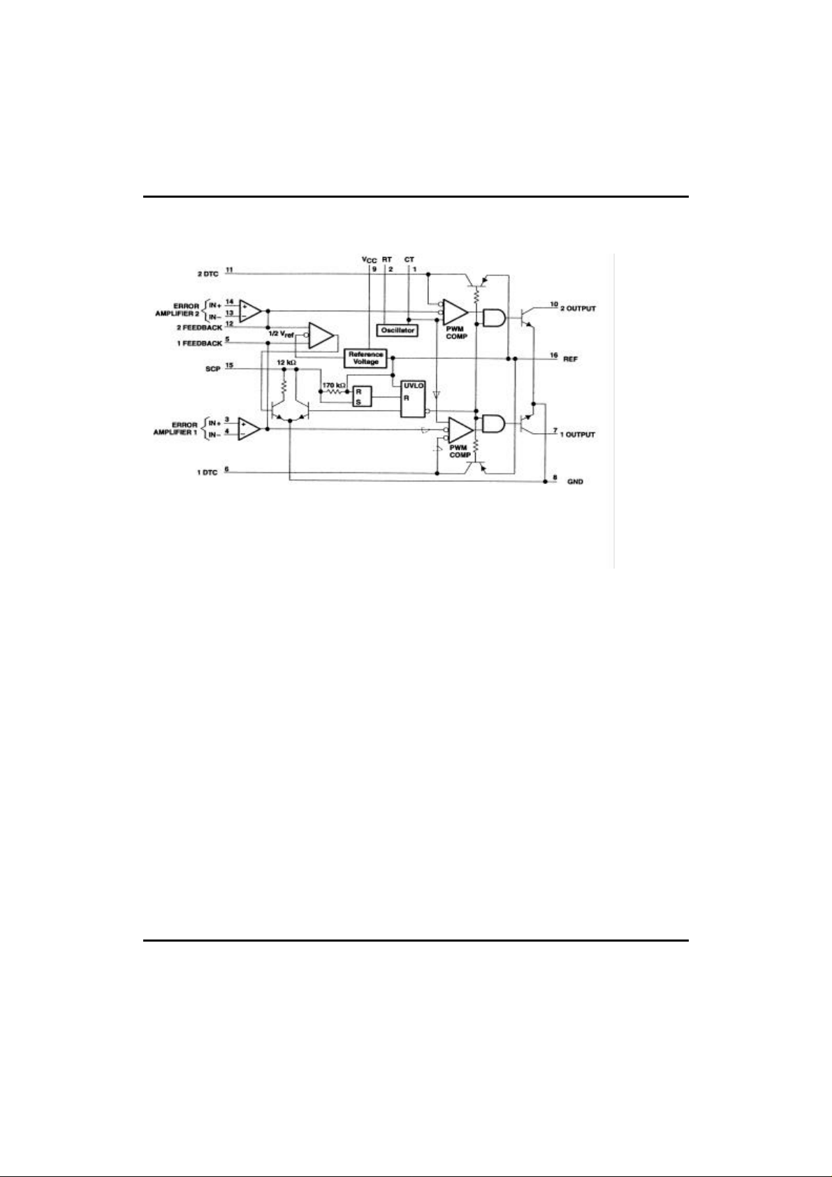
The UTC TL1451 incorporates on a single monolithic chip
all the functions required in the construction of two pulsewidth-modulation (PWM) control circuits. Designed primarily
for power supply control, the TL1451 contains an on-chip 2.5V
regulator, two error amplifiers, an adjustable oscillator, two
dead-time comparators, undervoltage lockout circuitry, and
dual common –emitter output transistor circuits.
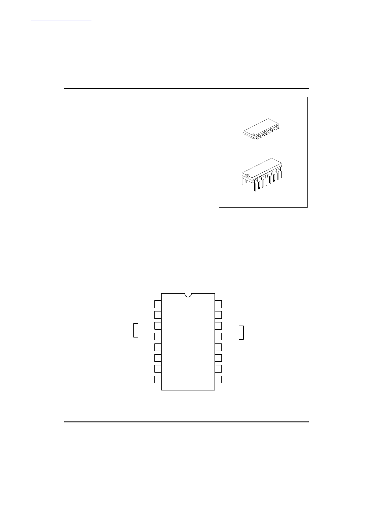
SOP-16
FEATURES
*Complete PWM Power control Circuitry
*Completely Synchronized Operation
*Internal Undervoltage Lockout Protection
*Wide Supply Voltage Range
*Internal Short-Circuit Protection
*Oscillator Frequency…500kHz Max
*Variable Dead Time Provides Control Over Total Range
*Internal Regulator Provides a Stable 2.5V Reference Supply
PIN CONFIGURATIONS
CT
1
2
RT
ERROR
AMPLIFIER
1
1 FEEDBACK
1 IN+
1 IN-
1 DTC
1 OUT
GND
3
4
5
6
7
8 9
16
15
14
13
12
11
10
REF
SCP
2 IN+
AMPLIFIER
2 IN-
2 FEEDBACK
2 DTC
2 OUT
Vcc
DIP-16
ERROR
2
UTC UNISONIC TECHNOLOGIES CO., LTD. 1
QW-R103-011,A
UTC TL1451 LINEAR INTEGRATED CIRCUIT
BLOCK DIAGRAM
UTC UNISONIC TECHNOLOGIES CO., LTD. 2
QW-R103-011,A

UTC TL1451 LINEAR INTEGRATED CIRCUIT
ABSOLUTE MAXIMUM RATINGS(Unless otherwise noted all is over operating free air temperature
range)
PARAMETER SYMBOL VALUE UNIT
Supply Voltage V
Amplifier Input Voltage V
Collector Output Voltage V
Collector Output Current I
Power Dissipation : TA≤25°C
DIP
SOP
Operating free-air Temperature Range TA -20 TO 85 °C
Storage Temperature Range Tstg -65 TO 150 °C
Lead Temperature 1.6mm from Case for 10
Sec.
CC
I
O
O
Tcase 260 °C
RECOMMENDED OPERATING CONDITIONS
PARAMETER SYMBOL VALUE UNIT
Supply Voltage Vcc 3.6 50 V
Amplifier Input Voltage Vi 1.05 1.45 V
Collector Output Voltage Vo 50 V
Collector Output Current(each Transistor) Io 20 mA
Current into Feedback Terminal 45 µA
Feedback Resistor RF 100 kΩ
Timing Capacitor CT 150 15000 pF
Timing Resistor RT 5.1 100 kΩ
Oscillator frequency 1 500 kHz
Operating Free-Air Temperature TA -20 85 °C
51 V
20 V
51 V
21 mA
mW
1000
500
MIN MAX
ELECTRICAL CHARACTERISTICS
(Over recommended operating free-air temperature range,VCC=6V,f=200kHz,TA=25°C ,Unless otherwise
specified)
PARAMETER TEST CONDITIONS MIN TYP MAX UNIT
Reference Section
Output Voltage Io=1mA 2.4 2.5 2.6 V
Output Voltage Change with Temperature TA=-20°C to 25°C
TA=25°C to 85°C
Input Voltage Regulation Vcc=3.6V to 40V 2 12.5 mV
Output Voltage Regulation Io=0.1mA to 1mA 1 7.5 mV
Short-Circuit Output Current Vo=0 3 10 30 mA
-0.1
-0.2
±1%
±1%
Undervoltage Lockout Section
Upper Threshold Voltage (Vcc) 2.72 V
Lower Threshold Voltage (Vcc) 2.6 V
Hysteresis (Vcc) 80 120 mV
Reset Threshold voltage (Vcc)
Io(ref)=0.1mA, TA=25°C
1.5 1.9 V
Short-Circuit Protection Control Section
Input Threshold Voltage(SCP) TA=25°C 0.65 0.7 0.75 V
UTC UNISONIC TECHNOLOGIES CO., LTD. 3
QW-R103-011,A

UTC TL1451 LINEAR INTEGRATED CIRCUIT
PARAMETER TEST CONDITIONS MIN TYP MAX UNIT
Standby Voltage(SCP) No pullup 140 185 230 mV
Latched Input Voltage (SCP) No pullup 60 120 mV
Input (source) Current VI=0.7V,TA=25°C -10 -15 -20 µA
Comparator Threshold Voltage (FEEDBACK) 1.18 V
Oscillator Section
Frequency CT=330pF, RT=10kΩ 200 kHz
Standard deviation of frequency CT=330pF, RT=10kΩ 10%
Frequency Change with Voltage Vcc=3.6V to 40V 1%
Frequency Change with Temperature TA=-20°C to 25°C
Dead-Time Control Section
Input bias Current (DTC) 1 µA
Latch mode (source) Current (DTC) TA=25°C -80 -145 µA
Latched Input Voltage (DTC) Io=40µA 2.3 V
Input threshold Voltage at f=10kHz (DTC) Zero duty cycle
Error-Amplifier Section
Input Offset Voltage Vo (FEEDBACK)=1.25V ±6 mV
Input Offset Current Vo (FEEDBACK)=1.25V ±100 nA
Input Bias current Vo (FEEDBACK)=1.25V 160 500 nA
Common-Mode Input Voltage Range Vcc=3.6V to 40V 1.05 to
Open-loop Voltage Amplification RF=200kΩ 70 80 dB
Unity-gain Bandwidth 1.5 MHz
Common-mode Rejection Ratio 60 80 dB
Positive Output Voltage Swing Vref-
Negative Output Voltage Swing 1 V
Output (sink) Current (FEEDBACK) VID=-0.1V,Vo=1.25V 0.5 1.6 mA
Output (source) Current (FEEDBACK) VID=-0.1V,Vo=1.25V -45 -70 µA
Output Section
Collector off-state Current Vo=50V 10 µA
Output Saturation Voltage Io=10mA 1.2 2 V
Short-Circuit Output Current Vo=6V 90 mA
PWM Comparator Section
Input Threshold Voltage at
f=10kHz (FEEDBACK)
TOTAL DEVICE
Standby Supply Current Off-state 1.3 1.8 mA
Average Supply Current RT=10kΩ 1.7 2.4 mA
TA=25°C to 85°C
Maximum duty cycle 1.2
Zero duty cycle
Maximum duty cycle 1.2
1.45
0.1
-0.4%
-0.2%
2.05
1.45
2.05
1.45
±2%
±2%
2.25 V
V
V
2.25 V
UTC UNISONIC TECHNOLOGIES CO., LTD. 4
QW-R103-011,A

UTC TL1451 LINEAR INTEGRATED CIRCUIT
TEST CIRCUIT
TIMING DIAGRAM
UTC UNISONIC TECHNOLOGIES CO., LTD. 5
QW-R103-011,A
 Loading...