

查询LMV393L-D08-T供应商
UNISONIC TECHNOLOGIES CO., LTD
LMV393
LINEAR INTEGRATED CIRCUIT
DUAL GENERAL PURPOSE,
LOW VOLAGE, COMPARATORS
DESCRIPTION
The UTC LMV393 is a low voltage (2.7-5V) version of the dual
comparators. Its noise performance has been improved by using
bipolar differential input and output stages. These comparators also
have a unique characteristic in that the input common-mode voltage
range includes ground even though operated from a single power
supply voltage.
The UTC LMV393 is designed for applications in consumer
automotive, mobile communications, notebooks and PDA’s, battery
powered electronics, General Purpose Portable Device, General
Purpose Low Voltage Applications.
FEATURES
* High precision comparator.
* Low operating voltage 2.7-5V.
* Low Supply Current 100μA/Channel (Typical).
* Low Input Bias Current 100nA (Typical).
* Low Input Offset Current 2nA (Typical).
* Input Common Mode Voltage Range Includes Ground.
* Low Output Saturation Voltage 0.2V.
*Pb-free plating product number: LMV393L
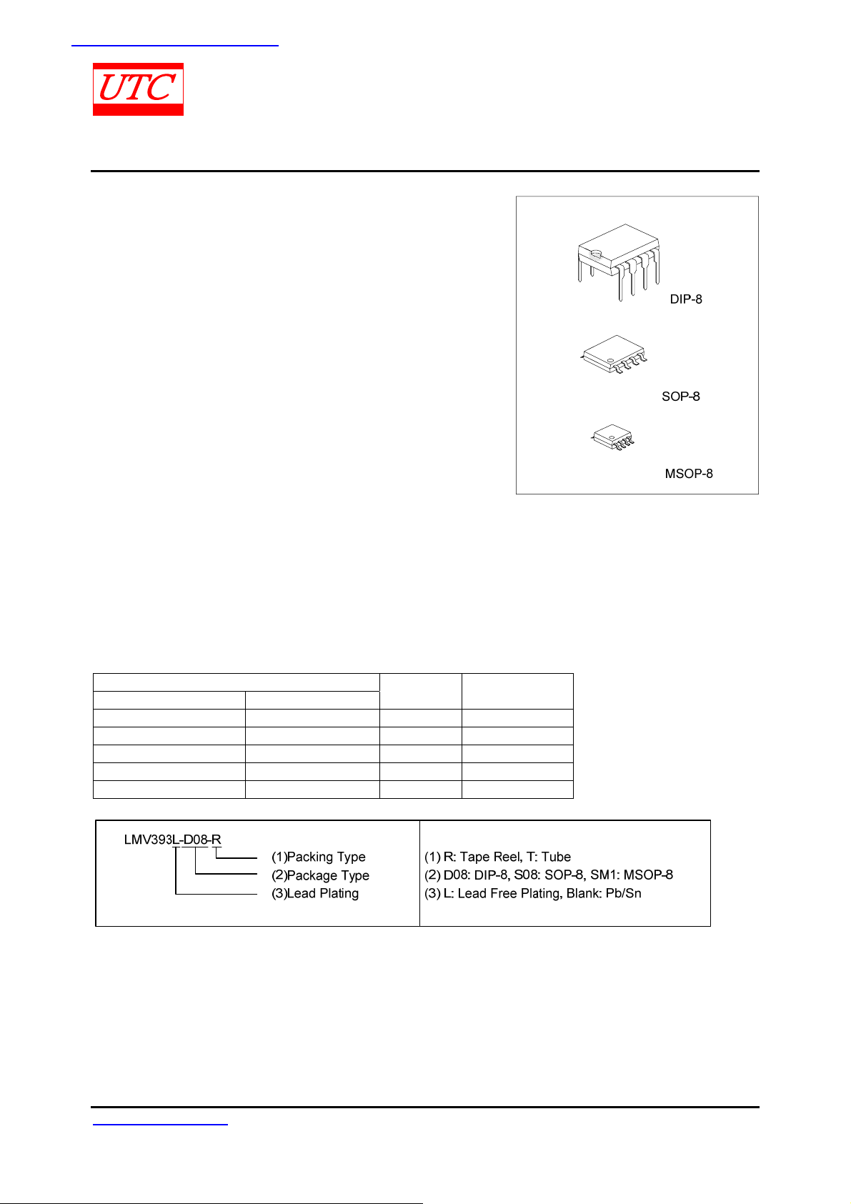
ORDERING INFORMATION
Ordering Number
Normal Lead Free Plating
LMV393-D08-T LMV393L-D08-T DIP-8 Tube
LMV393-S08-R LMV393L-S08-R SOP-8 Tape Reel
LMV393-S08-T LMV393L-S08-T SOP-8 Tube
LMV393-SM1-R LMV393L-SM1-R MSOP-8 Tape Reel
LMV393-SM1-T LMV393L-SM1-T MSOP-8 Tube
Package Packing
www.unisonic.com.tw 1 of 11
Copyright © 2005 Unisonic Technologies Co., Ltd QW-R104-004,A
LMV393 LINEAR INTEGRATED CIRCUIT
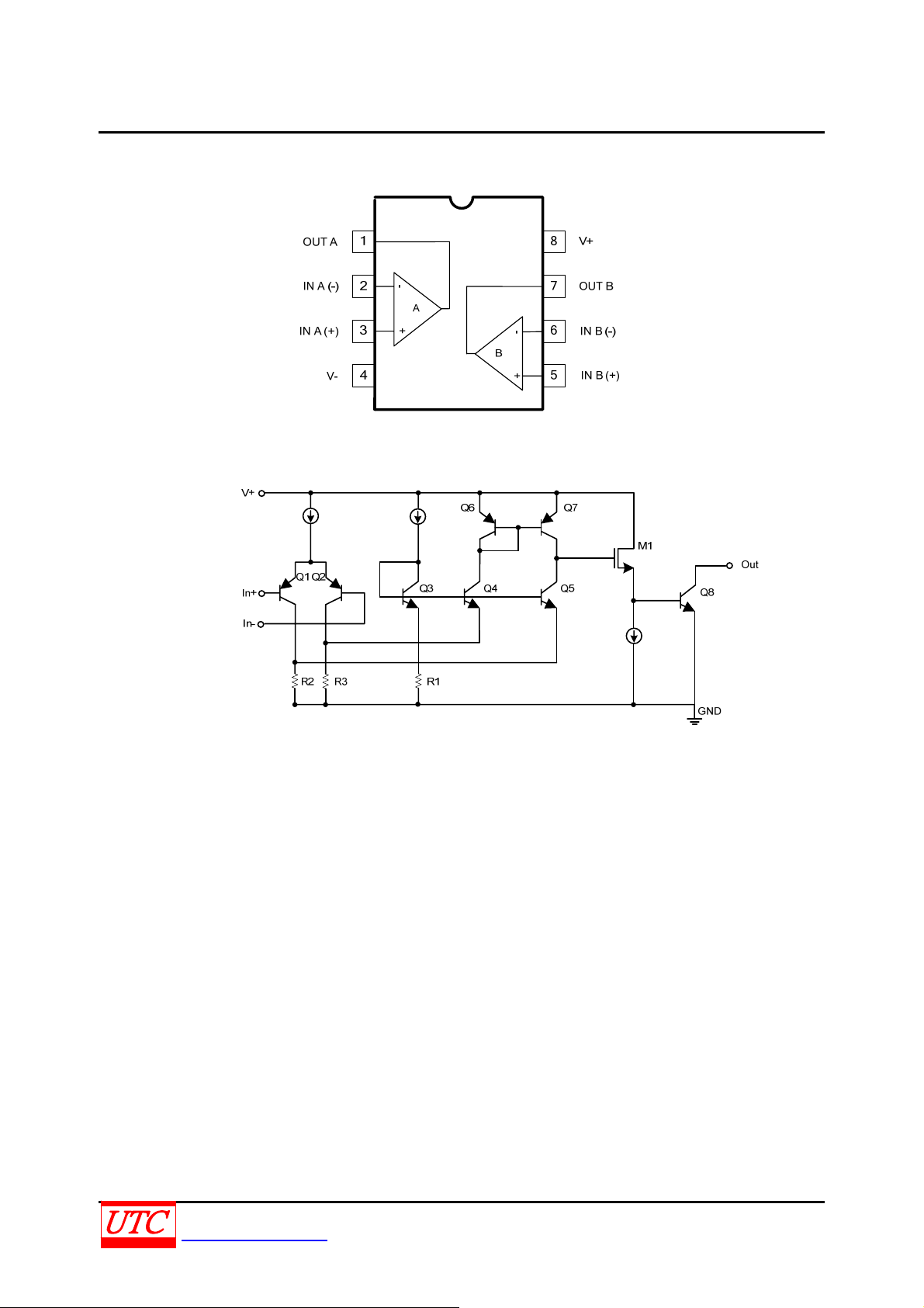
PIN CONFIGUREATION
BLOCK DIAGRAM
UNISONIC TECHNOLOGIES CO., LTD 2 of 11
www.unisonic.com.tw QW-R104-004,A
LMV393 LINEAR INTEGRATED CIRCUIT
ABSOLUTE MAXIMUM RATINGS
PARAMETER SYMBOL RATINGS UNIT
Supply Voltage VCC 2.7 ~ 5.0 V
Differential Input Voltage V
Voltage on any pin (referred to V- pin) 5.5 V
Junction Temperature TJ +150 °C
Operating Temperature T
Storage Temperature T
Note Absolute maximum ratings are those values beyond which the device could be permanently damaged.
Absolute maximum ratings are stress ratings only and functional device operation is not implied.
THERMAL CHARACTERISTICS
PARAMETER SYMBOL RATINGS UNIT
MSOP-8 190
Thermal Resistance Junction to Ambient
DC ELECTRICAL CHARACTERISTICS (T
PARAMETER SYMBOL TEST CONDITIONS MIN TYP MAX UNIT
Input Offset Voltage V
Input Offset Voltage Average Drift I
Input Bias Current I
Input Offset Current I
Input Voltage Range VIN
Supply Current ICC 100 200 μA
Voltage Gain GV 20 50 V/mV
Saturation Voltage V
Output Sink Current
2.7V 5 40
5.0V
Output Leakage Current I
IN(OFF)
I(OFF)
I(BIAS)
I(OFF)
SAT
I
SINK
LEAK
DIP-8 100
SOP-8
=25℃, V
J
1.7 7 mV
5 μV/℃
100 250 nA
2 50 nA
I
V
≤4mA 200 400 mV
SINK
≤1.5V
OUT
0.003 1 μA
±VCC V
IN(DIFF)
-40 ~ +85 °C
OPR
-65 ~ +150 °C
STG
θJA
℃/W
150
-
=0V, unless otherwise specified.)
-0.1
4.2
10 50
V
mA
AC ELECTRICAL CHARACTERISTICS (T
=25 ,℃ RL=5.1kΩ, V-=0V, unless otherwise specified.)
J
PARAMETER SYMBOL TEST CONDITIONS MIN TYP MAX UNIT
Propagation Delay
(High to Low)
Propagation Delay
(Low to High)
2.7V 9
5.0V
2.7V 3.8
5.0V
2.7V 2
5.0V
2.7V 0.7
5.0V
Input Overdrive=10mV
t
PHL
Input Overdrive=100mV
Input Overdrive=10mV
t
PLH
Input Overdrive=100mV
8
3.4
3
0.8
us
us
UNISONIC TECHNOLOGIES CO., LTD 3 of 11
www.unisonic.com.tw QW-R104-004,A
LMV393 LINEAR INTEGRATED CIRCUIT
APPLICATION CIRCUITS
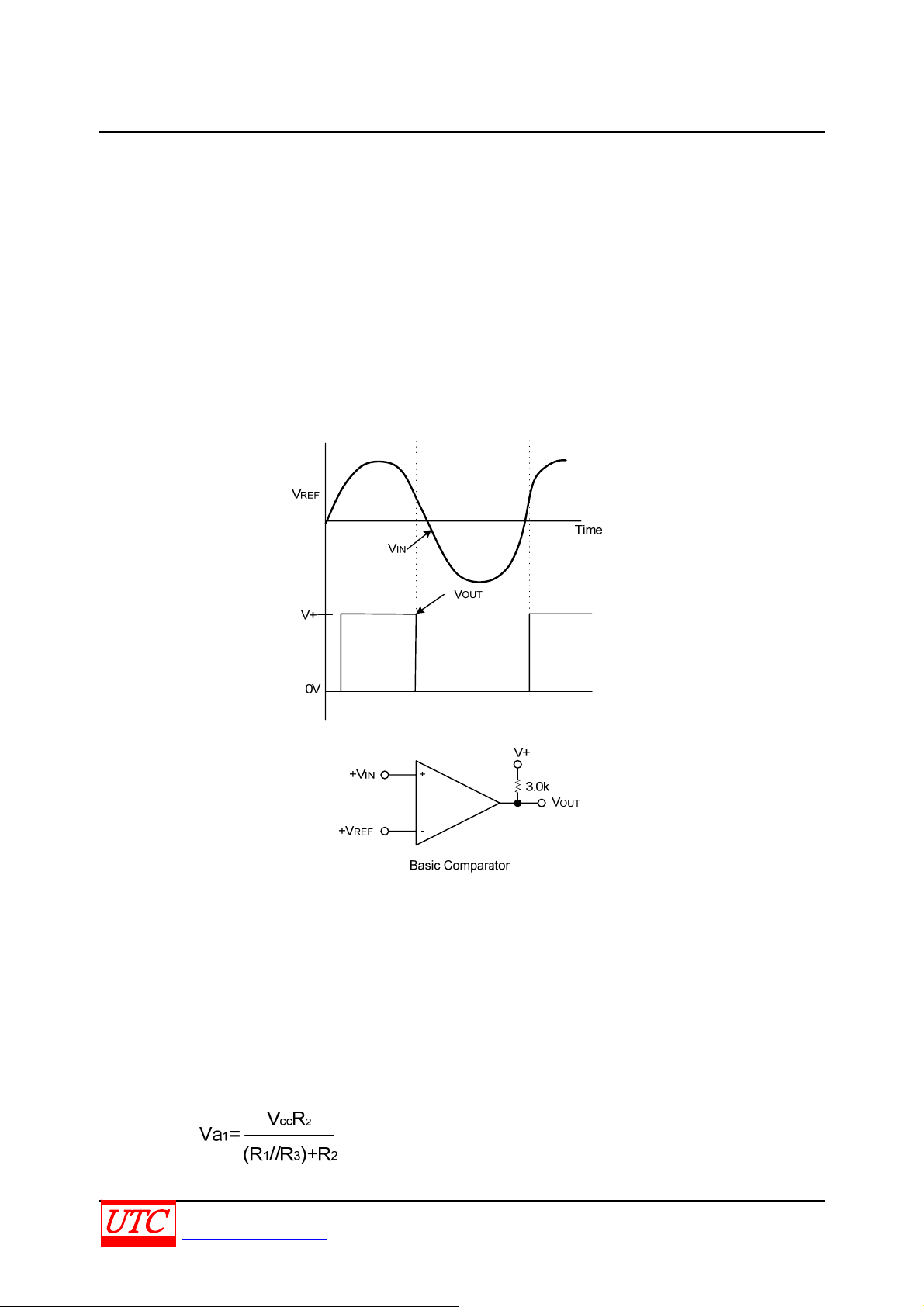
Basic Comparator
A basic comparator circuit can convert analog signals to a digital output. The UTC LMV393 needs a pull-up
resistor connected to the positive supply voltage which can make output switch properly. So that when the internal
output transistor is off, the output voltage will be pulled up to the external positive voltage.
The resister should be chosen properly. The higher resister can reduce the power dissipation. the lower resister
can improve the capacity of loading output. The range of resister should between 1k to 10kΩ.
The Output voltage of the comparator will be high if the input voltage at the non-inverting pin is greater than the
reference voltage at the inverting pin. On the other hand it will be low.
Comparator with Hysteresis
The comparator may oscillate or produce a noisy output if the applied differential input voltage is near the
comparator’s offset voltage, especially when the input signal is moving slowly across the comparator’s switching
threshold. Addition of hysteresis or positive feedback can solve this problem.
Inverting Comparator with Hysteresis
It requires a three resistor network that is referenced to the supply voltage V
voltage is high, these resistors can be represented as R1 // R3 in series with R2. The lower set input voltage is
defined as:
of the comparator. When the output
CC
UNISONIC TECHNOLOGIES CO., LTD 4 of 11
www.unisonic.com.tw QW-R104-004,A

LMV393 LINEAR INTEGRATED CIRCUIT
APPLICATION CIRCUITS(Cont.)
When V
upper trip voltage V
> Va the output voltage is low close to ground. It can be presented as R2 // R3 in series with R1. The
IN
is defined as
a2
The total hysteresis provided by the network is defined as:
To assure that the comparator will always switch correctly, the resistors values should be chosen as follow:
R
PULL-UP
<< R
and R1 > R
LOAD
PULL-UP
.
Non-Inverting Comparator with Hysteresis
It requires a two resistor network to implement a non inverting comparator with hysteresis and with a voltage
reference at the inverting input. So when V
V
must rise up to V
IN
, and V
IN1
can be calculated by:
IN1
is low, the output is also low. If the output will switch from low to high,
IN
When VIN is high, the output is also high, in order to make the comparator switch back to low, VIN can be
calculated by:
The hysteresis of this circuit is the difference between V
IN1
and V
IN 2
.
UNISONIC TECHNOLOGIES CO., LTD 5 of 11
www.unisonic.com.tw QW-R104-004,A

LMV393 LINEAR INTEGRATED CIRCUIT
APPLICATION CIRCUITS(Cont.)
Square Wave Oscillator
Comparators are suitable for oscillator applications. This application uses the minimum number of external
components. The output frequency is set by the RC time constant which is determined by capacitor C1 and the
resistor in the negative feedback R
rate and limit the maximum operating frequency.
C1
75pF
Vc
R1
Va
100k
+
V
R2
100k
of the comparator. Capacitive load at the output would degrade the output slew
4
+
V
Vc1
-Vcc
Va1
Va2
t = 0
R4
100k
-
+
R3
100k
4.3k
+
V
0
OUT
V
T
OUT
V
0
Squarewave Oscillator
At first, assume that the output is high, so the voltage at the inverting input VC is less than the voltage at the
non-inverting input Va, the capacitor C
input voltage V
V
will be given by:
a1
, the comparator output will switch.
a1
has to be discharged. When it has charged up to value equal to the positive
1
If: R1=R2=R3
Then:
When the output switches to ground, the value of Va is reset by the resistor network:
Then capacitor C1 discharge through a resistor towards ground. The output will return to its high state when the
voltage across the capacitor has discharged to a value equal to V
calculated from:
.The time to charge the capacitor can be
a2
Where V
One period will be given by: 1/freq = 2t or calculating the exponential gives: 1/freq = 2(0.694) R
and R
4
=2VCC/3 and VC = VCC/3
MAX
Resistors R3
4 C1
must be at least two times larger than R5 to insure a reasonable VO. The frequency stability of this circuit
should strictly be a function of the external components.
UNISONIC TECHNOLOGIES CO., LTD 6 of 11
www.unisonic.com.tw QW-R104-004,A

LMV393 LINEAR INTEGRATED CIRCUIT
APPLICATION CIRCUITS(Cont.)
Free Running Multivibrator
This oscillator circuit can generate a train of stable clock for precise timekeeping applications. We can obtain it by
using a resonator as the feedback component. A quartz crystal in its series-resonant mode can make the circuit
oscillating well. For the comparator be switching symmetrically about +V
equal. The RC time constant of R3 and C
frequency. When choose crystal, be sure to order series resonant with desired temperature coefficient.
is set to be several times greater than the period of the oscillating
1
/2, the value of R1 and R2 must choose
CC
Pulse generator with variable duty cycle:
A pulse generator with variable duty cycle can be obtained by creating two separated paths for C1 charge and
discharge into the basic square wave generator. One path, through R
pulse width (t
Varying resistor R
frequency of the generator.
The pulse width and time between pulses can be found from:
Where
And
then
). The other path, R1 and D1 will discharge the capacitor and set the time between pulses (t2).
1
, R2 can alter the time between pulses and the pulse width. Both controls also change the
1
tRC
−
−
tRC
CC
141
251
Fall time
CC
VV e
1max
VVe
1max
V =
max
V ==
1
1
(1 )
=− Rise time
=
2
V
3
VV
max
33
tRC
−
141
e
=
and D2 will charge the capacitor and set the
2
2
is then given by:
t
2
1
tRC
−
251
e
=
2
UNISONIC TECHNOLOGIES CO., LTD 7 of 11
www.unisonic.com.tw QW-R104-004,A

LMV393 LINEAR INTEGRATED CIRCUIT
APPLICATION CIRCUITS(Cont.)
V+
At last, we get,
141
251
ln 2tRC=
ln 2tRC=
These terms have a slight error because V
drop to:
max
2
()
CC BE
3
1
V
−
BE
1
V
−
BE
tRC
−
141
e
=
tRC
−
251
e
=
VVV=−
2(1 )
2(1 )
And that’s the exact value we get.
tRC V=−
141
tRC V=−
251
ln 2(1 )
ln2( 1 )
BE
BE
+
V
R1
1M
R2
100k
C1
80pF
R5
1M
-
+
R3
1M
R4
1M
is not exactly equal to 2/3 VCC but is actually reduced by the diode
max
*FOR LARGE RATIOS OF R1/R2.
D1 CAN BE OMITTED.
Pulse Generator
15k
D1
*
D2
+
6μs60μs
tot1
VOUT
-V
0
t2
UNISONIC TECHNOLOGIES CO., LTD 8 of 11
www.unisonic.com.tw QW-R104-004,A

LMV393 LINEAR INTEGRATED CIRCUIT
APPLICATION CIRCUITS(Cont.)
Positive Peak Detector:
Positive peak detector is basically the comparator operated as a unit gain follower with a large holding capacitor
from the output to ground. Additional transistor is added to the output to provide a low impedance current source.
When the output of the comparator goes high, current is passed through the transistor to charge up the capacitor.
The only discharge path will be the 1M ohm resistor shunting C1 and any load that is connected to the output. The
decay time can be altered simply by changing the 1MΩ resistor. The output should be used through a high
impedance follower to a avoid loading the output of the peak detector.
Negative Peak Detector:
For the negative detector, the output transistor of the comparator acts as a low impedance current sink. The only
discharge path will be the 1MΩ resistor and any load impedance used. Decay time is changed by varying the 1MΩ
resistor.
UNISONIC TECHNOLOGIES CO., LTD 9 of 11
www.unisonic.com.tw QW-R104-004,A

LMV393 LINEAR INTEGRATED CIRCUIT
TYPICAL CHARACTERISTICS
1700
1600
1500
1400
1300
1200
1100
1000
Output Voltage (mV)
Output Voltage vs Output Current at 5V Supply
+85℃
900
800
700
600
500
400
300
200
100
0
0
10
Output Current (mA)
20
30
+25℃
40
50
Output Voltage vs Output Current at 2.7 Supply
700
600
500
+85℃
400
300
Output Voltage (mV)
200
100
0
0
5
10
Output Current (mA)
+25℃
15
20
250
200
150
100
50
Input Bias Current (nA)
5
0
2.5
5
4
3
VOUT (V)
2
Output Voltage
1
0
~
~
0
Input Bias Current vs Supply Voltage
VIN=0V
+25℃
+85℃
3.5
Supply Voltage (V)
Response Time for Input Overdrive Positive Transition
100mV
20mV
Overdrive
5mV
4.5
Vcc=5V
Ta=25℃
R
L=5.1kΩ
5.5
~
~
Response Time vs Input Overdrives Negative
5
4
3
VOUT (V)
2
Output Voltage
1
0
~
~
100
IN (mV)
V
0
Input Voltage
Response Time vs Input Overdrives Negative
3
2
1
VOUT (V)
Output Voltage
0
~
~
100
100mV 20m
Overdrive
0
0.5
100m
V
Transition
V
1.5
1
Time (μs)
Transition
20mV
Vcc=5V
Ta=25℃
R
L=5.1kΩ
2
Vcc=2.7V
Ta=25℃
R
L=5.1kΩ
10mV
2.5
10mV
~
~
3
~
~
(mV)
-100
Input Voltage
0
3
6
Time (μs)
9
12
IN (mV)
V
0
Input Voltage
Overdrive
0
0.5
1
Time (μs)
1.
2
5
UNISONIC TECHNOLOGIES CO., LTD 10 of 11
www.unisonic.com.tw QW-R104-004,A

LMV393 LINEAR INTEGRATED CIRCUIT
TYPICAL CHARACTERISTICS (Cont.)
OUT (V)
V
Output Voltage
(mV)
Input Voltage
UTC assumes no responsibility for equipment failures that result from using products at values that
exceed, even momentarily, rated values (such as maximum ratings, operating condition ranges, or
other parameters) listed in products specifications of any and all UTC products described or contained
herein. UTC products are not designed for use in life support appliances, devices or systems where
malfunction of these products can be reasonably expected to result in personal injury. Reproduction in
whole or in part is prohibited without the prior written consent of the copyright owner. The information
presented in this document does not form part of any quotation or contract, is believed to be accurate
and reliable and may be changed without notice.
UNISONIC TECHNOLOGIES CO., LTD 11 of 11
www.unisonic.com.tw QW-R104-004,A
 Loading...