


UTC L2800 LINEAR INTEGRATED CIRCUIT
SWITCHING REGULATOR
CONTROLLER(LOW VOLTAGE)
DESCRIPTION
The UTC L2800 is a single-channel switching
regulator control IC for low voltage applications
incorporating a soft start function and short circuit
detection function. The device has a low minimum
operating voltage of 1.8V and is ideal for the power
supply of battery-operated electronic equipment.
FEATURES
*Wide supply voltage operating range: 1.8V~15V
*Low current consumption: Typically 5.5mA in
operation,1µA or less in stand-by
*High speed operation is possible: Maximum 1MHz
*The error amplifier gain is set inside the IC,so
peripheral components are minimized.
*Incorporates a soft start circuit.
*Incorporates a timer-latch type short circuit detection
circuit (SCP).
*Totem-pole type output with adjustable on/off current
(for NPN transistors)
*Incorporates a stand-by function.
PIN CONFIGURATION
SOP-8
TSSOP-8
-IN 1
SCP
Vcc
BR/CTL
2
3
4
FB
8
OSC
7
6
GND
5
OUT
UTC UNISONIC TECHNOLOGIES CO., LTD.
QW-R121-010,A
1
UTC L2800 LINEAR INTEGRATED CIRCUIT
PIN DESCRIPTION
PIN NO. SYMBOL I/O DESCRIPTION
1 -IN I Error amplifier inverting input pin
2 SCP - Soft start and SCP setting capacitor connection pin
3 VCC - Power supply pin
4 BR/CTL I Output current setting and control pin
5 OUT O Totem-pole type output pin
6 GND - Ground pin
7 OSC - Capacitor and resistor connection pin for setting the oscillation frequency
8 FB O Error amplifier output pin
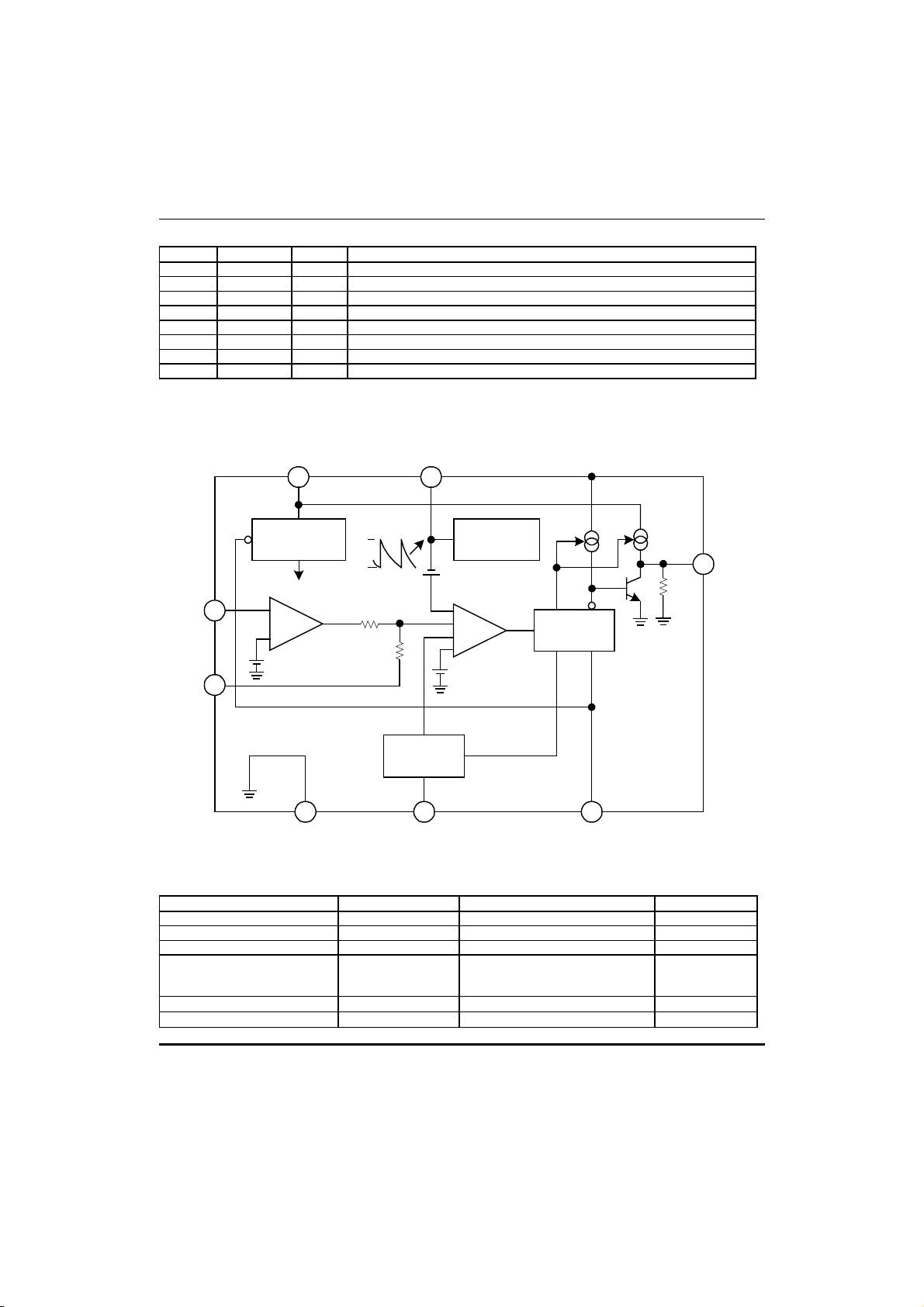
BLOCK DIAGRAM
Vcc OSC
3 7
-IN
FB
Reference
voltage supply
1.25V
1
8
-
+
Error Amp.
0.5V
6 2 4
0.6V
0.1V
36kΩ
500Ω
Soft start
SCP
Sawtooth
wave oscillator
0.1V
PWM
Comp.
+
+
+
DTC 0.6V
Output drive
control circuit
0.3V
BR/CTLSCPGND
30kΩ
5
OUT
ABSOLUTE MAXIMUM RATINGS (Ta=25℃)
Power Supply Voltage Vcc 16 V
Output Source Current IO+ -50 mA
Output Sink Current IO- 50 mA
Power Dissipation
Storage Temperature Tstg -55 ~ +125
Operating Temperature Top -30 ~ +85
* When mounted on a 10cm square double-sided epoxy board.
PARAMETER SYMBOL RATINGS UNIT
SOP-8
TSSOP-8
PD
570*
580*
mW
°C
°C
UTC UNISONIC TECHNOLOGIES CO., LTD.
QW-R121-010,A
2

UTC L2800 LINEAR INTEGRATED CIRCUIT
RECOMMENDED OPERATING CONDITIONS (Ta=25°C)
PARAMETER SYMBOL MIN TYP MAX UNIT
Power Supply Voltage Vcc 1.8 15 V
Error Amplifier Input Voltage VI -0.2 1.0 V
BR/CTL Pin Input Voltage VBR -0.2 Vcc V
Output Source Current IO+ -40 mA
Output Sink Current IO- 40 mA
SCP Pin Capacitance CPE 0.1
Phase Compensation Capacitance CP 0.1
Output Current Setting Resistance RB 150 390 5000
Timing Resistance RT 1.0 3.0 10.0
Timing Capacitance CT 100 270 10000 pF
Oscillation Frequency fosc 10 500 1000 kHz
Operating Temperature Top -30 +25 +85
ELECTRICAL CHARACTERISTICS
PARAMETER SYMBOL TEST CONDITIONS MIN TYP MAX UNIT
Circuit to prevent
malfuncition at low input
oltage (U.V.L.O)
Soft Start
Short Circuit
Detection(S.C.P.)
Sawtooth Wave
Oscillator(OSC)
Error Amplifier
Idle Period Adjustment
Section
Output Section
Reset Voltage VR 0.9 V
Threshold Voltage VTH
Charging Current Ics VSCP=0V -1.5 -1.0 -0.7
Voltage at soft start
completion
Charging Current Icpc VSCP=0V -1.5 -1.0 -0.7
Threshold Voltage VtPC 0.7 0.8 0.9 V
Oscillation Frequency
Frequency Input
Stability
Frequency Variation
With Temperature
Input Threshold Voltage VT VFB=450mV 480 500 520 mV
VT Input Stability VTdV Vcc=2V ~ 15V 5 20 mV
VT Variation With
Temperature
Input Bias Current IB VIN=0V -1.0 -0.2 1.0
Voltage Gain Av 70 100 145 V/V
Frequency Bandwidth BW AV=0dB 6 MHz
Voltage Range
Output Source Current IOM+ -40 -24
Output Sink Current I
Maximum Duty Cycle tDUTY
Output Voltage
Output Source Current IO+
Output Sink Current IOPull Down Resistance RO 20 30 40
(Ta=25°C, VCC=+2V)
Vts 0.7 0.8 0.9 V
fosc
RT=3.0kΩ, CT=270pF
fdV Vcc=2V ~ 15V 2 10 %
fdT
Ta=-30°C ~ +85°C
Ta=-30°C ~ +85°C
VTdT
VOM+ 0.78 0.87 V Maximum Output
OM
V
OM
VOH1
VOH2
VOL1
VOL2
-
V
FB=0.45V
-
R
T=3.0kΩ, CT=270pF
VFB=0.8V
RB=390Ω, Io=-15mA
RB=750Ω, Vcc=1.8V
Io= -10mA
RB=390Ω, Io=15mA
RB=750Ω, Vcc=1.8V
Io=10mA
RB=390Ω, Vo=0.9V
RB=390Ω, Vo=0.3V
1.1 1.3 1.5 V
400 500 600 kHz
5 %
1 %
0.05 0.2 V
24 40
65 75 85 %
1.0 1.2 V
0.8 1.0 V
0.1 0.2 V
0.1 0.2 V
-30 -20 mA
30 60 mA
µF
µF
Ω
kΩ
°C
µA
µA
µA
µA
µA
kΩ
UTC UNISONIC TECHNOLOGIES CO., LTD.
QW-R121-010,A
3

UTC L2800 LINEAR INTEGRATED CI RCUIT
PARAMETER SYMBOL TEST CONDITIONS MIN TYP MAX UNIT
Output Current Setting
Section/Control Section
Entire Device
DIAGRAM
FB pin voltage
Reference input for short
circuit detection comparator
Idle period setting voltage
Sawtooth wave output
Soft start setting voltage
OUT pin waveforms
SCP pin waveforms
Pin Voltage VBR
RB=390Ω
Input Off Condition IOFF -20 0
Input On Condition ION -45
Pin Current Range IBR
Stand-by Current ICCS BR/CTL pin open or Vcc 1
Average Supply Current ICC
RB=390Ω
0.2 0.3 0.4 V
µA
µA
-1.8 -0.1 mA
µA
5.5 9.3 mA
tPE
Output short circuit
Short circuit
detection
Power supply control SW
OFF
Soft start
ts
ON
Output
short
circuit
HOW TO SET THE TIME CONSTANT FOR SOFT START AND SHORT CIRCUIT
DETECTION
1.SOFT START
At power on, the capacitor CPE connected to the SCP pin starts charging. The PWM comparator compares the
soft start setting voltage as a proportion of the voltage at the SCP pin with the sawtooth waveform. The
comparison controls the ON duty of the OUT pin, causing the soft start operation. On completion of soft start
operation, the voltage at the SCP pin stays low, the soft start setting voltage stays high, and the circuit enters the
output short circuit detection wait state.
Soft start time (The time until the output ON duty reaches approximately 50%)
ts[S]≒0.35*C
PE[µF]
2.SHORT CIRCUIT PROTECTION
If the switching regulator output suddenly drops due to load effect, the error amplifier output (FB pin) is fixed at
VOM+ and capacitor CPE starts charging. When the voltage at the SCP pin reaches approximately 0.8V,the output
pin is set low and the SCP pin stays low.
Once the protection circuit operates, the circuit can be restored by resetting the power supply.
• Short circuit detection time
tPE[S]≒0.8*CPE[µF]
UTC UNISONIC TECHNOLOGIES CO., LTD.
QW-R121-010,A
4

UTC L2800 LINEAR INTEGRATED CI RCUIT
TYPICAL CHARACTERISTICS
Supply Voltage vs.Supply Current
10
8
6
4
Supply current ,Icc (mA)
2
0
0
4
81216
Supply voltage ,Vcc ( V )
Supply Voltage vs.Input Threshold Voltage
1.0
0.8
0.6
0.4
0.2
Input threshold voltage ,V T (V)
0
0
1.0
2.0
Supply voltage ,Vcc ( V )
Ta=+25℃
B=390Ω
R
Ta=+25℃
3.0 4.0 5.0
20
1.0
0.8
0.6
0.4
0.2
,ΔVT/VT (%)
-10
Input threshold voltage variation ration
-15
Supply Voltage vs.Input Threshold Voltage
0
0
4
81216
Supply voltage ,Vcc ( V )
Ambient Temperature vs. Input Threshold
10
5
0
-5
-40
Voltage Variation Ratio
-20
0
20 40 60 80 1 00
Ambient temperature ,Ta ( ℃)
Ta=+25℃
20
Vcc=2V
High Level Output
2.0
1.6
1.2
0.8
0.4
Low level output voltage ,V OUT (V)
0
-10
0
-20 -30 -40 -50
High level output current ,I OUT(mA)
Vcc=2V
Ta=+25℃
B=390Ω
R
500
400
300
200
100
Low level output voltage ,V OUT (mV) Input threshold Voltage ,V T (V)
0
0
Low Level Output
Vcc=2V
Ta=+25℃
B=390Ω
R
20
40 60
High level output current ,I OUT(mA)
80
100
UTC UNISONIC TECHNOLOGIES CO., LTD.
QW-R121-010,A
5

UTC L2800 LINEAR INTEGRATED CI RCUIT
BR/CTL Pin Current vs. Output Source Current
-50
-40
-30
-20
-10
Output source current ,I OUT (mA)
0
-0.40-0.8 -1.2
BR/CTL pin Current ,I BR (mA)
BR/CTL Pin Current vs. Supply Current
5.0
4.0
3.0
2.0
Supply current ,I CC (mA)
1.0
0
-20
0
-40
BR/CTL pin current ,I
-60
BR (μA)
Vcc=2V
V
OUT=0.9V
Ta=+25℃
-1.6 -2.0
Vcc=2V
Ta=+25℃
-80
500
400
300
200
100
BR/CTL pin voltage ,VBR (mV)
0
0
1M
500k
200k
100k
50k
20k
10k
Oscillation frequency ,fosc (Hz)
5k
-100
2k
BR/CTL Pin Current vs. BR/CTL Pin Voltage
Vcc=2V
Ta=+25℃
-0.4
Timing Resistor vs. Oscillation Frequency
CT=100pF
CT=1000pF
CT=10000pF
1k
-0.8
BR/CTL pin current ,I BR (mA)
2k 5k 10k
Timing resistor ,R T (Ω)
-1.2 -1.6
Vcc=2V
Ta=+25℃
-2.0
20k
Supply Voltage vs. Frequency Variation Ratio
10
-5
-10
Frequency variation ratio ,Δf/f (%)
-15
5
0
02
46
Supply voltage ,Vcc (V)
8
10
CT=270pF
Ta=+25℃
R
T=3.0kΩ
12 14 16
UTC UNISONIC TECHNOLOGIES CO., LTD.
QW-R121-010,A
Ambient Temperature vs. Frequency Variation Ratio
10
5
0
-5
-10
Frequency variation ratio ,Δf/f (%)
-15
-40
-20
0
20 40
Ambient temperature ,Ta (℃)
Vcc=2V
C
T=270pF
R
T=3.0kΩ
60
100
80
6

UTC L2800 LINEAR INTEGRATED CI RCUIT
Oscillation Frequency vs.Maximum Duty Cycle
100
80
60
40
20
Maximum duty cycle, tDUTY (%)
0
10K
Output Pin Voltage and Current Waveforms (Reference Data)
(V)
2V
6
4
VOUT
2
0
(mA)
50
IOUT
0
-50
10mV 200ns
0.4 0.8 1.2 1.6 2.0
0
Note:The OFF delay time of VOUT depends on
the characteristics of the external transistor.
100K 1M
Oscillation frequency ,fosc (Hz)
Vcc=2V
C
T=270pF
Ta=+25℃
Vcc
22μH
Vcc=2V
C
T=270pF
R
T=1.0kΩ
t
(μs)
(5V)
UTC L2800
4
5
IOUT
OUT
V
10μF
18kΩ
2kΩ
390Ω
-IN
Measurement Circuit Diagram
UTC UNISONIC TECHNOLOGIES CO., LTD.
QW-R121-010,A
7

UTC L2800 LINEAR INTEGRATED CI RCUIT
FUNCTIONAL DESCRIPTION
1. SWITCHING REGULATOR FUNCTION
(1) REFERENCE VOLTAGE CIRCUIT
The reference voltage circuit generates a temperature-compensated reference voltage(≒1.25V)from voltage
supplied from the power supply pin(pin 30).In addition to providing the reference voltage for the switching
regulator, the circuit also sets the idle period.
(2) SAWTOOTH WAVE OSCILLATOR
The sawtooth oscillator generates a sawtooth wave(up to 1 MHz)that is stable with respect to the supply
voltage and temperature. The capacitor and resistor that set the oscillation frequency are connected to the
OSC pin(pin 7).
(3) ERROR AMPLIFIER (ERROR AMP.)
The error amplifier detects the output voltage of the switching regulator and outputs the PWM control signal.
The voltage gain is fixed, and connecting a phase compensation capacitor to the FB pin(pin 8)provides stable
phase compensation for the system.
(4) PWM COMPARATOR (PWM COMP.)
The voltage comparator has one inverting and three non-inverting inputs. The comparator is a voltage /pulse
width converter that controls the ON time of the output pulse depending on the input voltage. The output level
is high(H) when the sawtooth wave is lower than the error amplifier output voltage, soft start setting voltage,
and idle period setting voltage.
(5) OUTPUT CIRCUIT
The output circuit has a totem pole type configuration and can drive an external NPN transistor directly. The
value of the ON/OFF current can be set by a resistor connected to the BR/CTL pin(pin 4).
2. POWER SUPPLY CONTROL FUNCTION
Stand-by mode(supply current 1µA or less) can be set by connecting the BR/CTL pin(pin 4) to Vcc or by
making the pin open circuit.
SW MODE
OFF Stand-by mode
ON Operating mode
UTC L2800
4
RB
BR/CTL
SW
3. OTHER FUNCTIONS
(1) SOFT START AND SHORT CIRCUIT DETECTION
Soft start operation is set by connecting capacitor CPE to SCP pin(pin 2).Soft start prevents a current spike on
start-up.
On completion of soft start operation, the SCP pin(pin 2) stays low and enters the short circuit detection wait
state. When an output short circuit occurs, the error amplifier output is fixed at VOM+ and capacitor CPE starts
charging. After charging to approximately 0.8V,the output pin(pin 5) is set low and the SCP pin(pin 2) stays low.
Once the protection circuit operates, the circuit can be restored by resetting the power supply.(See “HOW TO
SET THE TIME CONSTANT FOR SOFT START AND SHORT CIRCUIT DETECTION”)
UTC UNISONIC TECHNOLOGIES CO., LTD.
QW-R121-010,A
8

UTC L2800 LINEAR INTEGRATED CI RCUIT
(2) CIRCUIT TO PREVENT MALFUNCTION AT LOW INPUT VOLTAGE
Transients when powering on or instantaneous glitches in the supply voltage can lead to malfunction of the
control IC and cause system damage or failure. The circuit to prevent malfunction at low input voltage detects a
low input voltage by comparing the supply voltage to the internal reference voltage. On detection, the circuit
fixes the output pin to low.
The system recovers when the supply voltage rises back above the threshold voltage of the malfunction
prevention circuit.
APPLICATION EXAMPLE
18kΩ
22μH
1
SCP
IN
V
3V
UTC assumes no responsibility for equipment failures that result from using products at values that
exceed, ev en momentarily, rated values (such as maximum ratings, operating condition ranges, or
other parameters) listed in products specifications of any and all UTC products described or contained
herein. UTC products are not designed for use in life support appliances, dev ices or systems where
malfunction of these products can be reasonably expected to result in personal injury. Reproduction in
whole or in part is prohibited without the prior written consent of the copyright owner. The information
presented in this document does not form part of any quotation or contract, is believed to be accurate
and reliable and may be changed without notice.
33μF
2kΩ
BR/CTL
0.1μF
CTL
Vcc
2
3
4
390Ω
FB-IN
8
OSC
7
GND
6
OUT
5
0.1μF
270pF
3kΩ
10μF
V
5V
O
UTC UNISONIC TECHNOLOGIES CO., LTD.
QW-R121-010,A
9
 Loading...