

UNISEM US3033CS Datasheet
US3033
PWM SWITCHER & LINEAR
CONTROLLER IC
FEATURESFEATURES
LDO Controller allows the use of a low cost
pass transistor for the I/O supply
8 pin SOIC combines switching and linear
controller
Internal Pre-regulator Eliminates Cross talk
between Switching & Linear regulators
Automatic shut down of the linear regulator
when connected to the Vcc2 Det pin
On board MOSFET driver
Fastest transient response of any controller
method. ( 0 to 100% Duty Cycle in 100 nS )
1% internal voltage reference
Internal Under Voltage Lockout protects
MOSFET during start-up
APPLICATIONSAPPLICATIONS
Dual supply low voltage processor applications,
such as: P55C,CYRIX M2, POWER PC and
AMD K6
Simple 5V to 3.3V switcher for Pentium with AGP
or Pentium II applications
DESCRIPTIONDESCRIPTION
The US3033 IC combines a switching controller and
a linear regulator controller all in a compact 8 pin
surface mount package, providing a total solution for
dual supply processor applications such as an Intel
P55C , AMD K6, as well as Cyrix 6X86L and
the M2processors. Typically in these applications a
dual supply regulator converts 5V to 3.3V for I/O supply
and a jumper programmable supply of 1.25V to 3.5V for
CORE supply .The linear regulator controller portion in
the US3033 is a programmable controller allowing flexibility for the I/O regulator and has a minimum of 50mA
drive current capability designed to provide ample current for an external pass transistor. The IC uses an internal regulator generated from the 12V supply to power
the controller as well as the 12V supply to drive the power
MOSFET, allowing a low cost N channel MOSFET
switch to be used. The IC also includes an error comparator for fast transient response, a precise voltage reference for setting the output voltage as well as a direct
drive of the MOSFET for the minimum part count.
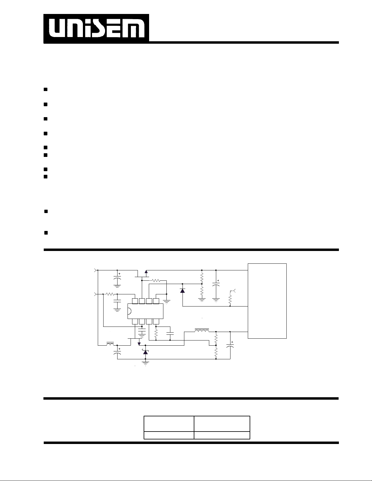
TYPICAL APPLICATIONTYPICAL APPLICATION
C1
C8
Drv1V12swVfb1Vhyst
1 2 3 4
C3
Q2
Q1
US3033
R10
5678
GndVfb2Drv2V12
D1C2
R3 C5
R6
C6
D2
R7
L2
R4
R5
5V
R9
12V
L1
Typical application of US3033 in a flexible mother board designed for Intel P55,P54
AMD K5,K6 as well as Cyrix M1 and M2 applications.
Notes: P54C,P55C,Pentium II are trade marks of Intel Corp. K5 & K6 are trade marks of AMD corp. Cyrix 6X86L,M1,M2 are trade marks
of Cyrix Corp. Power PC is trade mark of IBM Corp.
I / O
5V
R8
C7
CPU
Vcc2 Det
Core
3033app1-1.1
PACKAGE ORDER INFORMATIONPACKAGE ORDER INFORMATION
TA (°C) 8 PIN PLASTIC
SOIC (S)
0 TO 70 US3033CS
Rev. 1.5
1/14/99
4-1
US3033
ABSOLUTE MAXIMUM RATINGSABSOLUTE MAXIMUM RATINGS
V12,V12SW Supply Voltages ............................................................. 20V
F.B Pin Voltages........................................................ -0.3V to 5V
Storage Temperature Range ................................. -65 TO 150°C
Operating Junction Temperature ............................... 0 TO 150°C
PACKAGE INFORMATIONPACKAGE INFORMATION
8 PIN PLASTIC SOIC (S)
TOP VIEW
1
Drv1
2
V12sw
3
Vfb1
4
Vhyst Gnd
θJA =160°C/W
8
V12
7
Drv2
6
Vfb2
5
ELECTRICAL SPECIFICATIONSELECTRICAL SPECIFICATIONS
Unless otherwise specified the following specification applies over V12 =V12SW =12V, and TA =0 to 70°C. Low duty
cycle pulse testing are used which keeps junction and case temperatures equal to the ambient temperature.
Linear Controller Section
PARAMETER SYM TEST CONDITION MIN TYP MAX UNITS
F.B Voltage Initial Accuracy VFB2 TJ =25°C, Drv2=VFB2, CL=100uF 1.237 1.250 1.262 V
F.B Voltage Total Variation Drv2=VFB2, CL=100uF 1.225 1.250 1.275 V
F.B Voltage Line Regulation 10<V12<14V,Drv2=VFB2, CL=100uF 0.2 %
F.B Input Bias Current IFB2 VFB2 =1.25V -1 +1 uA
Maximum Drive Current IDRVMAX VFB2 =1V, VFB1 =1.5V 50 mA
V12 Supply Current I12 VFB2 =1V, VFB1 =1.5V, IDRV2 =0 5 mA
Switching Controller Section
PARAMETER SYM TEST CONDITION MIN TYP MAX UNITS
F.B Voltage Initial Accuracy VFB1 TJ =25°C 1.237 1.250 1.262 V
F.B Voltage Total Variation 1.225 1.250 1.275 V
F.B Voltage Line Regulation 0.2 %
F.B Input Bias Current IFB1 VFB1 =1.25V -1 +1 uA
Min On Time VFB1 is sq wave with 300 ns on 800 nS
time and 2 uS off time
Min Off Time VFB1 is sq wave with 300 ns off 800 nS
time and 2 uS on time
Vhyst pin output-HI ISOURCE =500uA, VFB1 =1.5V 11 V
Vhyst pin output-LO ISINK =500uA, VFB1 =1V 1 V
Supply Current I12SW VFB1 =1V , VFB2 =1.5V 10 mA
Maximum Duty Cycle DMAX VFB1 =1V 100 %
Minimum Duty Cycle DMIN VFB1 =1.5V 0 %
Gate Drive Rise/Fall Time VGATE Load=IRL3303 70 nS
4-2
Rev. 1.5
1/14/99
PIN DESCRIPTIONSPIN DESCRIPTIONS
PIN # PIN SYMBOL PIN DESCRIPTION
3 VFB1
6 VFB2
7 Drv2
5 Gnd
1 Drv1
4 VHYST
2 V12SW
8 V12
A resistor divider from this pin to the output of the switching regulator and ground sets the
Core supply voltage.
The feedback pin of the linear regulator. A resistor divider from this pin to the output of the
linear regulator and ground sets the I/O supply voltage.
The drive pin of the linear regulator. This pin controls the base of a transistor or the gate
of a MOSFET acting as the series pass element for the linear regulator.
This pin is connected to the IC substrate and must be connected to the lowest potential
in the system.
The PWM output of the switching controller. This pin is a totem pole drive that is connected to the gate of the power MOSFET. A resistor may be placed from this pin to the
gate in order to reduce switching noise.
A resistor and a 10pF capacitor is connected from this pin to the VFB1 pin to set the
output ripple voltage for the switching regulator.
This pin supplies the voltage to the PWM drive and hysterises circuitry and it is connected to the 12V supply. A 1 uF, high frequency capacitor must be connected from this
pin to ground to provide the peak current for charging and discharging of the MOSFET.
This pin provides the biasing for the chip and drive for the linear regulator controller. It
isconnected to 12V supply. A 10 ohm resistor in series from this pin to the 12V supply
and a 1uF, high frequency capacitor connected from this pin to Gnd is required to filter
the switching noise of the switching regulator.
US3033
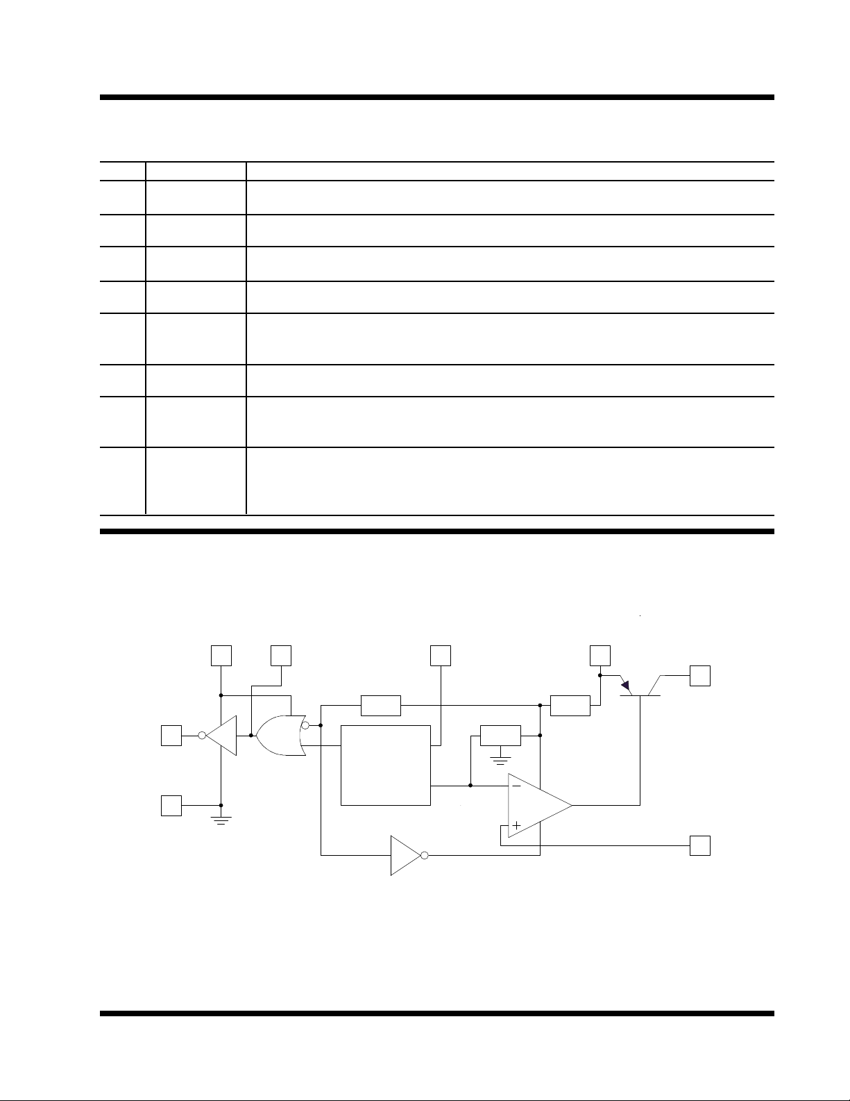
BLOCK DIAGRAMBLOCK DIAGRAM
V12sw Vhyst
2 4 3
Drv 1
1
Gnd
5
Vfb 1
UVLO
Vref
PWM Control
3033blk1-1.0
Figure 1 - Simplified block diagram of the US3033
1.25V
5V Reg
V12
8
Drv 2
7
Vfb2
6
Rev. 1.5
1/14/99
4-3
 Loading...