

UNISEM US3021BCW Datasheet
5 BIT PROGRAMMABLE SYNCHRONOUS BUCK
FEATURESFEATURES
Provides Single Chip Solution for Vcore,
GTL+ ,AGP Bus, and 1.8V
Automatic Voltage Selection for AGP slot
Vddq supply
Linear regulator controller on board for 1.8V
Designed to meet Intel Latest VRM specification for next generation micrprocessors
On board DAC programs the output voltage
from 1.3V to 3.5V
Linear regulator controller on board for 1.5V
GTL+ supply
Loss less Short Circuit Protection for all
outputs
Synchronous operation allows maximum
efficiency
Patented architecture allows fixed frequency
operation as well as 100% duty cycle during
dynamic load
Minimum part count
Soft Start
High current totem pole driver for direct
driving of the external Power MOSFET
Power Good function Monitors all Outputs
OVP Circuitry Protects the Switcher Output
and generates a Fault output
APPLICATIONSAPPLICATIONS
Total Power Soloution for Next Generation Intel
Processor application
US3021B
PLUS TRIPPLE LDO CONTROLLER
PRELIMINARY DATASHEET
DESCRIPTIONDESCRIPTION
The US3021B controller IC is specifically designed to
meet Intel specification for next generation microprocessor applications requiring multiple on board regulators . The US3021B provides a single chip control-
ler IC for the Vcore , 3LDO controllers, one with the
automatic select pin that connects to the TYPE DETECT pin of the AGP slot for the AGP Vddq supply,
one for GTL+ and the other for the 1.8V chip set
regulator as required for the next generation PC
applications. The US3021B typically uses Bipolar
transistors for Vout3(1.5V) and Vout4(1.8V) however
if Vaux pin is connected to 12V, then MOSFETs can
also be used as external pass elements. No external resistor divider is necessary for any of the regulators. The switching regulator feature a patented topol-
ogy that in combination with a few external components
as shown in the typical application circuit ,will provide
well in excess of 20A of output current for an on- board
DC/DC converter while automatically providing the right
output voltage via the 5 bit internal DAC .The US3021B
also features, loss less current sensing for both
switcher by using the Rds-on of the high side Power
MOSFET as the sensing resistor, an output under
voltage shutdown that detects short circuit condition for the linear outputs and latches the system
off, and a Power Good window comparator that switches
its open collector output low when any one of the outputs is outside of a pre programmed window.
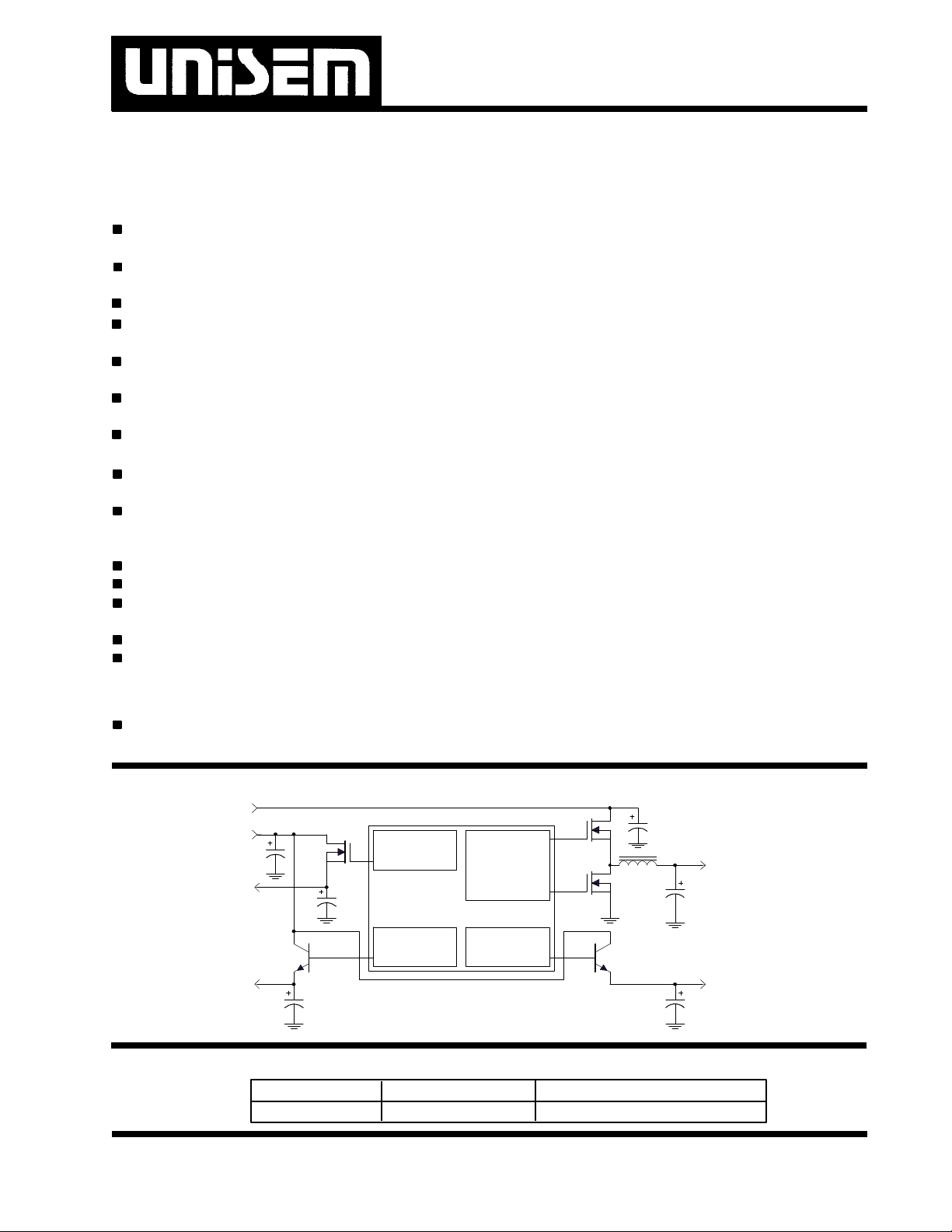
TYPICAL APPLICATIONTYPICAL APPLICATION
5V
3.3V
Vout2
Vout3
LINEAR
CONTROL
US3021B
LINEAR
CONTROL
PACKAGE ORDER INFORMATIONPACKAGE ORDER INFORMATION
Ta (°C) Device Package
0 TO 70 US3021BCW 28 pin Plastic SOIC WB
Rev. 1.4
12/8/00
SWITCHER
CONTROL
LINEAR
CONTROL
3021Bapp3-1.1
Vout1
Vout4
4-1
US3021B
ABSOLUTE MAXIMUM RATINGSABSOLUTE MAXIMUM RATINGS
V5 supply Voltage ........................................... 7V
V12 Supply Voltage ............................................ 20V
Storage Temperature Range ................................. -65 TO 150°C
Operating Junction Temperature Range .......... 0 TO 125°C
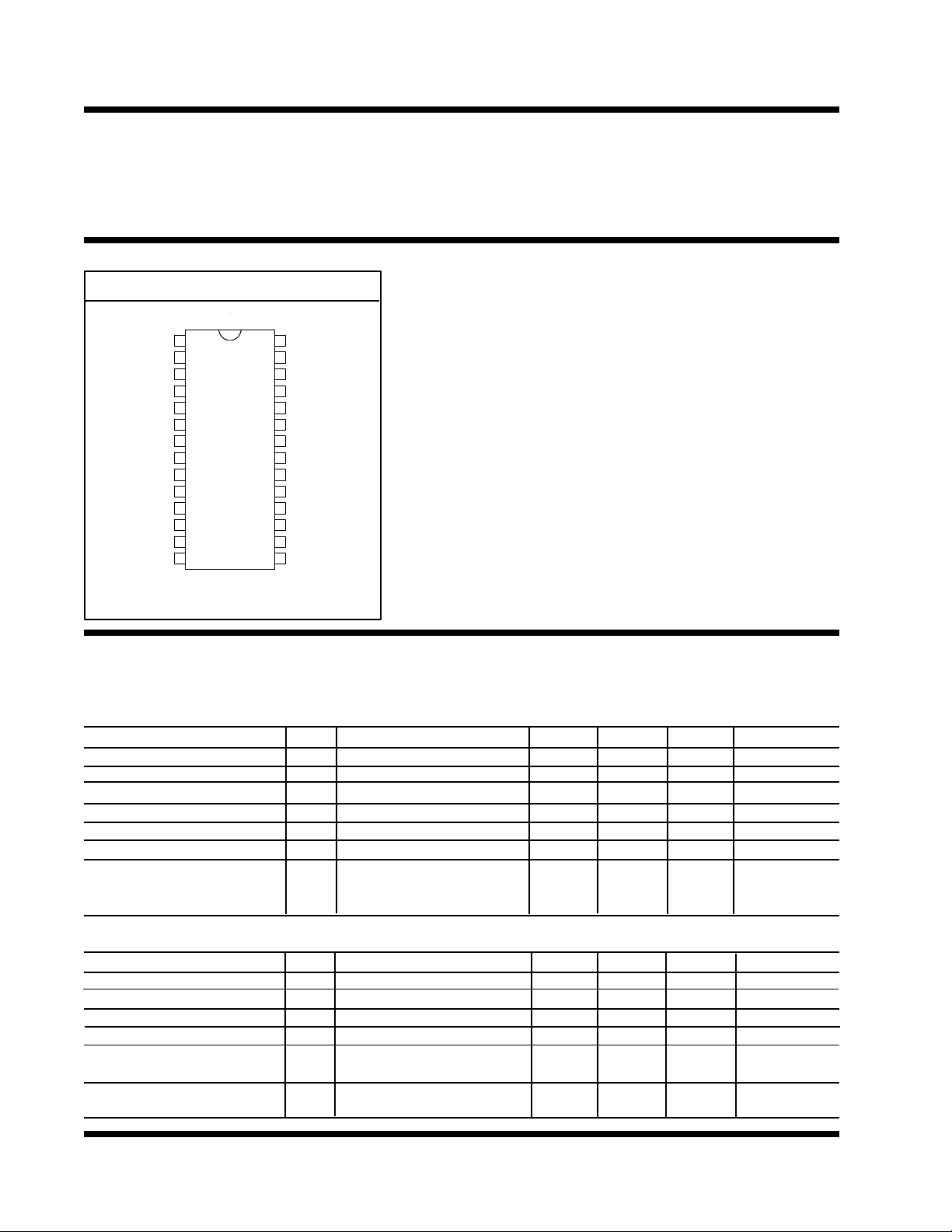
PACKAGE INFORMATIONPACKAGE INFORMATION
28 PIN WIDE BODY PLASTIC SOIC (W)
TOP VIEW
1
Drive2
2
Fix
3
VID4
4
VID3
5
VID2
6
VID1
7
VID0
8 21
PGood
9 20
SD
10 19
Vsen2
11 18
Select
12 17
SS
13 16
Fault / Rt
14
Vsen4 Drive4
28
27
26
25
24
23
22
15
V12
UGate
Phase
LGate
PGnd
OCSet
Vsen1
Fb
V5
Vsen3
Drive3
Gnd
Vaux
θJA =80°C/W
ELECTRICAL SPECIFICATIONSELECTRICAL SPECIFICATIONS
Unless otherwise specified ,these specifications apply over ,V12 = 12V, V5 = 5V and Ta=0 to 70°C. Typical values
refer to Ta =25°C. Low duty cycle pulse testing are used which keeps junction and case temperatures equal to the
ambient temperature.
PARAMETER SYM TEST CONDITION MIN TYP MAX UNITS
Supply UVLO Section
UVLO Threshold-12V Supply ramping up 10 V
UVLO Hysterises-12V 0.6 V
UVLO Threshold-5V Supply ramping up 4.4 V
UVLO Hysterises-5V 0.3 V
Supply Current
Operating Supply Current
V12 6 mA
V5 30
Switching Controllers; Vcore (Vsen 1) and AGP (Vsen 2)
VID Section (Vcore only)
DAC output voltage (note 1) 0.99Vs Vs 1.01Vs V
DAC Output Line Regulation 0.1 %
DAC Output Temp Variation 0.5 %
VID Input LO 0.8 V
VID Input HI 2 V
VID input internal pull-up
resistor to V5 27 kΩ
Vsen2 Voltage Select<0.8V 1.5 V
Select>2V 3.3 V
4-2
Rev. 1.4
12/8/00
US3021B
Error Comparator Section
Input bias current 2 uA
Input Offset Voltage -2 +2 mV
Delay to Output Vdiff=10mV 100 nS
Current Limit Section
C.S Threshold Set Current 200 uA
C.S Comp Offset Voltage -5 +5 mV
Hiccup Duty Cycle Css=0.1 uF 10 %
Output Drivers Section
Rise Time CL=3000pF 70 nS
Fall Time CL=3000pF 70 nS
Dead band Time Between
High side and Synch Drive
(Vcore Switcher Only) CL=3000pF 200 nS
Oscillator Section (internal)
Osc Frequency Rt=Open 217 Khz
1.8V Regulator (Vsen 4)
Vsense Voltage Vo4 Ta=25, Drive4 = Vsen4 1.800 V
Vsense Voltage 1.800 V
Input bias current 2 uA
Output Drive Current Vaux-Vdrive>0.6V 50 mA
1.5V Regulator (Vsen 3)
Vsense Voltage Vo3 Ta=25, Drive3 = Vsen3 1.500 V
Vsense Voltage 1.500 V
Input bias current 2 uA
Output Drive Current Vaux-Vdrive>0.6V 50 mA
Power Good Section
Vsen1 UV lower trip point Vsen1 ramping down 0.90Vs V
Vsen1 UV upper trip point Vsen1 ramping up 0.92Vs V
Vsen1 UV Hysterises .02Vs V
Vsen1 HV upper trip point Vsen1 ramping up 1.10Vs V
Vsen1 HV lower trip point Vsen1 ramping down 1.08Vs V
Vsen1 HV Hysterises .02Vs V
Vsen2 trip point Select<0.8V 1.100 V
Select>2V 2.560 V
Vsen4 trip point Fix=GND 0.920 V
Fix=Open 1.320 V
Vsen3 trip point Fix=GND 0.920 V
Fix=Open 1.140 V
Power Good Output LO RL=3mA 0.4 V
Power Good Output HI RL=5K pull up to 5V 4.8 V
Fault (Overvoltage) Section
Core O.V. upper trip point Vsen1 ramping up 1.17Vs V
Core O.V. lower trip point Vsen1 ramping down 1.15Vs V
FAULT Output HI Io=3mA 10 V
Soft Start Section
Soft Start Current OCset=0V , Phase=5V 20 uA
Rev. 1.4
12/8/00
4-3
 Loading...