

Uniks P1203BV Schematics
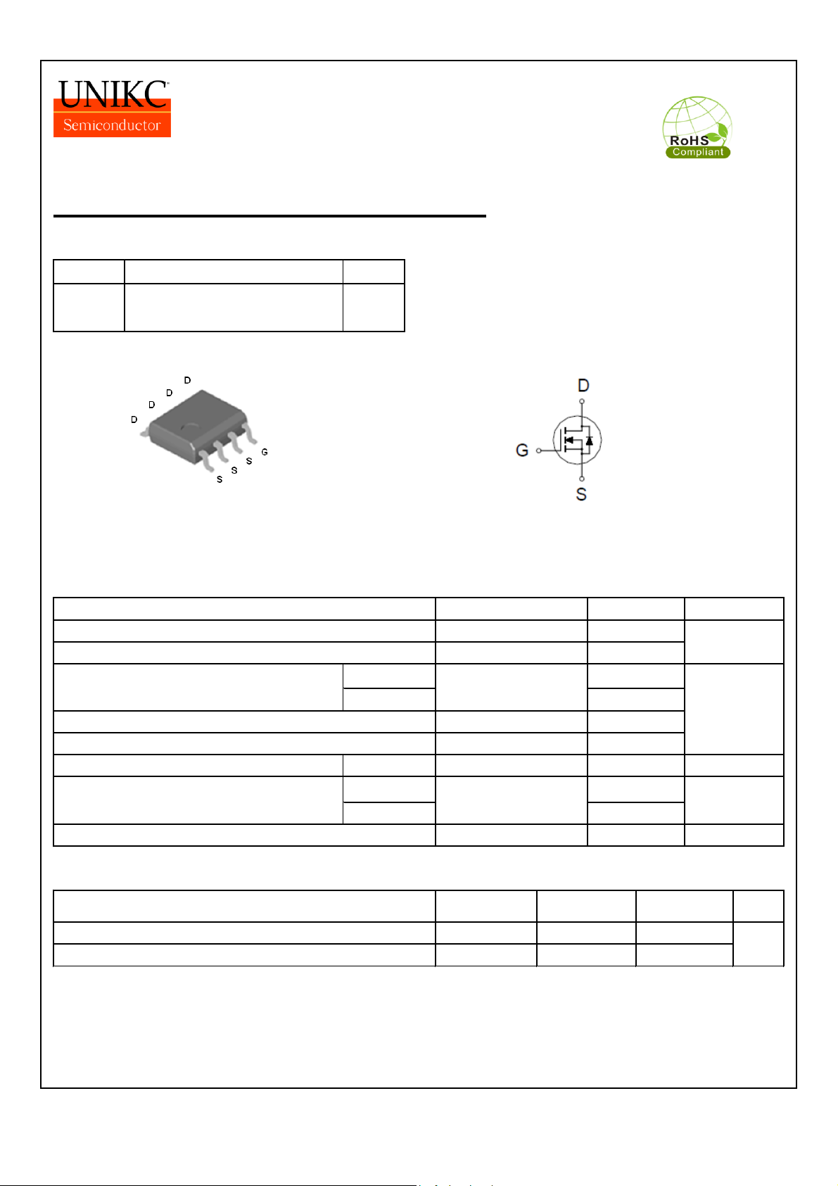
P1203BV
N-Channel Enhancement Mode MOSFET
PRODUCT SUMMARY
V
(BR)DSS
SOP- 08
ABSOLUTE MAXIMUM RATINGS (TA = 25 °C Unless Otherwise Noted)
THERMAL RESISTANCE RATINGS
UNITS
1
Pulse width limited by maximum junction temperature.
2
Limited only by maximum temperature allowed
A
mJ3040
28
SYMBOL
I
D
I
DM
1
2.5
W
THERMAL RESISTANCE
R
qJC
TYPICAL
UNITS
40
711±20
Continuous Drain Current
2
VGSV
DS
LIMITS
V
TA = 25 °C
Operating Junction & Storage Temperature Range
TA = 100 °C
Power Dissipation
Junction-to-Ambient
MAXIMUM
R
DS(ON)
TA = 100 °C
PARAMETERS/TEST CONDITIONS
Drain-Source Voltage
Gate-Source Voltage
I
D
12mΩ @V
GS
= 10V
11A
Avalanche Energy
L = 0.1mH
Pulsed Drain Current
1 , 2
TA = 25 °C
Avalanche Current
30V
°C
-55 to 150
50
IASE
AS
SYMBOL
P
D
TJ, T
STG
Junction-to-Case
25
R
qJA
°C / W
Ver 1.0 1 2012/4/13
P1203BV
N-Channel Enhancement Mode MOSFET
ELECTRICAL CHARACTERISTICS (TJ = 25 °C, Unless Otherwise Noted)
MIN TYP MAX
30
1 1.8 3
±100 nA
1
10
70 A
14 17.5
8.5 12
40 S
846
225
126
1.65 Ω
17
2.7494020
6
1.9 A
1.3 V
21 nS
10 nC
1
Pulse test : Pulse Width 300 msec, Duty Cycle 2%.
2
Independent of operating temperature.
VGS = 0V, VDS = 0V, f = 1MHz
Zero Gate Voltage Drain Current
Forward Transconductance
1
g
fs
VDS = 5V, ID = 10A
DYNAMIC
Input Capacitance
C
iss
mA
I
DSS
VDS = 20V, VGS = 0V , TJ = 125 °C
VGS = 0V, VDS = 20V, f = 1MHz
pF
mΩ
Output Capacitance
C
oss
VDS = VGS, ID = 250mA
VDS = 0V, VGS = ±20V
STATIC
Gate-Body Leakage
Gate Threshold Voltage
I
GSS
VGS = 0V, ID = 250mA
V
(BR)DSSVDS
= 24V, VGS = 0V
TEST CONDITIONS
V
LIMITS
UNIT
Drain-Source Breakdown Voltage
V
GS(th)
Reverse Transfer Capacitance
C
rss
Total Gate Charge
2
Q
g
PARAMETER
SYMBOL
Gate Resistance
R
g
On-State Drain Current
1
I
D(ON)
VDS = 0.5V
(BR)DSS
,
ID = 8.8A, V
GS
= 10V
nC
Gate-Source Charge
2
Q
gs
Gate-Drain Charge
2
Q
gd
VDD = 15V, ID = 12.5A, VGS = 10V,
RG=6Ω
nS
Rise Time
2
t
r
Turn-Off Delay Time
2
t
d(off)
Fall Time
2
t
f
Reverse Recovery Time
t
rr
IF = 11 A, dlF/dt = 100A / mS
Reverse Recovery Charge
Q
rr
SOURCE-DRAIN DIODE RATINGS AND CHARACTERISTICS (TJ = 25 °C)
Continuous Current
ISVDS = 10V, VGS = 10V
Drain-Source On-State
Resistance
1
VGS = 10V, ID = 11A
R
DS(ON)
VGS = 4.5V, ID = 11A
Forward Voltage
1
V
SDIF
= 25A, VGS = 0V
Turn-On Delay Time
2
t
d(on)
Ver 1.0 2 2012/4/13
 Loading...