

Uniks P0903BEA Schematics
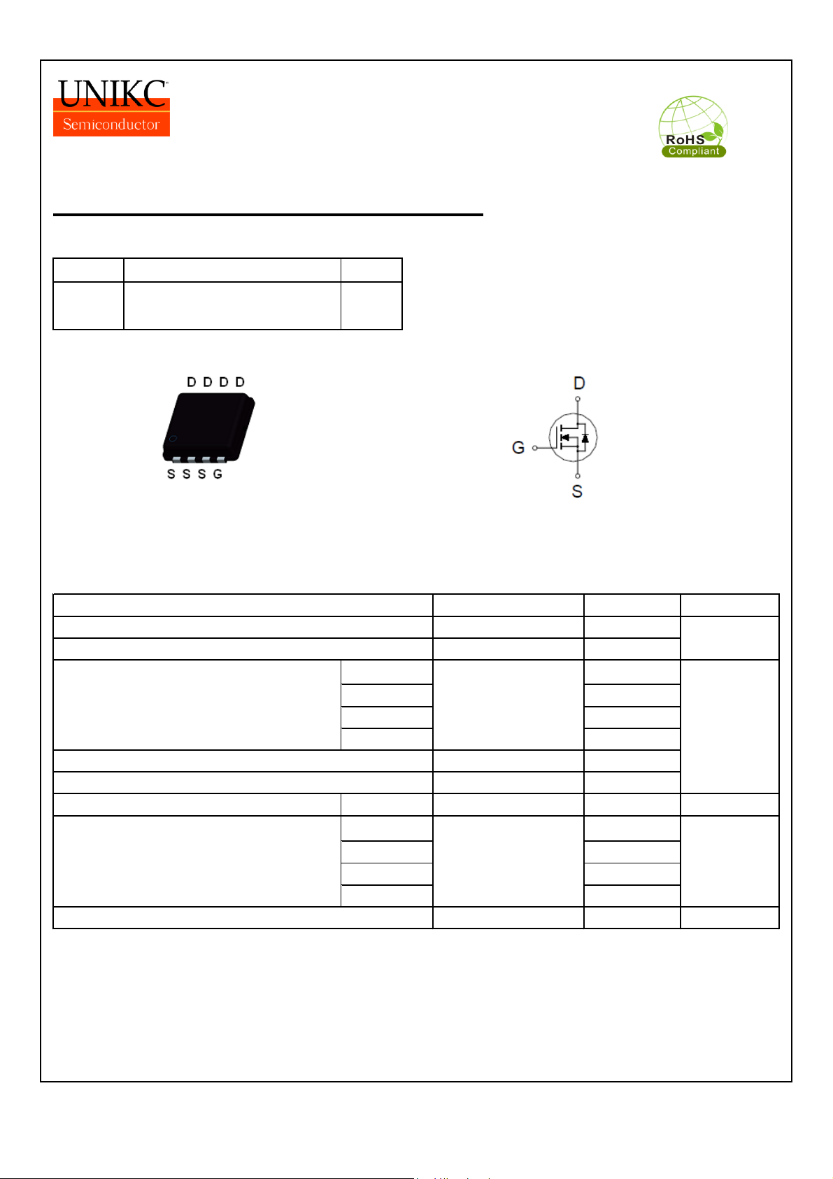
P0903BEA
N-Channel Enhancement Mode MOSFET
PRODUCT SUMMARY
V
(BR)DSS
PDFN 3x3P
ABSOLUTE MAXIMUM RATINGS (TA = 25 °C Unless Otherwise Noted)
R
DS(ON)
TC = 100 °C
PARAMETERS/TEST CONDITIONS
Drain-Source Voltage
Gate-Source Voltage
9mΩ @V
GS
= 10V
48A
SYMBOL
V
DS
Pulsed Drain Current
1
45
30
Operating Junction & Storage Temperature Range
I
D
30V
W
Avalanche Current
I
AS
TC = 25 °C
E
AS
L = 0.1mH
TJ, T
STG
TC = 25 °C
TC = 100 °C30V
GS
1.5
13
33
I
DM
48
30102.3
±20
I
D
P
D
13
TA = 70 °C
Avalanche Energy
LIMITS
°C
-55 to 150
mJ
UNITS
130
V
A
Continuous Drain Current
2
Power Dissipation
TA = 25 °C
TA = 70 °C
TA = 25 °C
Ver 1.0 1 2012/9/4
P0903BEA
N-Channel Enhancement Mode MOSFET
THERMAL RESISTANCE RATINGS
UNITS
1
Pulse width limited by maximum junction temperature.
2
Package limitation current is 30A.
3
The value of R<JA is measured with the device mounted on 1in2 FR-4 board with 2oz.Copper , in a still air
environment with TA=25°C。The value in any given application depends on the user's specific board design
ELECTRICAL CHARACTERISTICS (TJ = 25 °C, Unless Otherwise Noted)
MIN TYP MAX
30
1 1.7 3
±100 nA
1
10
130
A
11.2 13
7 9
45 S
1590
193
159
31175.581.7 Ω
91432
16
VDS = 5V, VGS = 10V
Drain-Source On-State
Resistance
1
R
DS(ON)
VGS = 10V, ID = 13A
t
f
Fall Time
2
Reverse Transfer Capacitance
QgdQ
gs
nS
VDS = 0.5V
(BR)DSS
,
ID @ 13A, VGS = 10V, R
GEN
= 3Ω
Gate Resistance
t
d(on)trtd(off)RgVGS
= 0V, VDS = 0V, f = 1MHz
THERMAL RESISTANCE
SYMBOL
TYPICAL
Input Capacitance
Output Capacitance
Gate-Drain Charge
2
Gate-Source Charge
2
PARAMETER
SYMBOL
TEST CONDITIONS
LIMITS
MAXIMUM
UNIT
R
qJA
VGS = 4.5V, ID = 10A
VDS = 5V, ID = 13A
V
GS(th)
Forward Transconductance
1
VGS = 0V, ID = 250mA
V
(BR)DSS
Zero Gate Voltage Drain Current
Gate-Body Leakage
gfsI
D(ON)
nC
VGS = 0V, VDS = 15V, f = 1MHz
pF
C
issCoss
Q
g(VGS=10V)
VDS = 0.5V
(BR)DSS
, ID = 13A,
VGS=10V
C
rss
Gate Threshold Voltage
DYNAMIC
V
I
GSS
I
DSS
mA
VDS = 24V, VGS = 0V
mΩ
On-State Drain Current
1
Drain-Source Breakdown Voltage
VDS = 20V, VGS = 0V , TJ = 55 °C
VDS = VGS, ID = 250mA
VDS = 0V, VGS = ±20V
STATIC
55
R
qJC
3.7
Total Gate Charge
2
Q
g(VGS=4.5V
Turn-On Delay Time
2
Rise Time
2
Turn-Off Delay Time
2
Junction-to-Ambient
3
Junction-to-Case
°C / W
Ver 1.0 2 2012/9/4

P0903BEA
N-Channel Enhancement Mode MOSFET
48 A
1.3 V
11.7 nS
2 nC
1
Pulse test : Pulse Width 300 msec, Duty Cycle 2%.
2
Independent of operating temperature.
3
Package limitation current is 30A.
Forward Voltage
1
V
SD
Reverse Recovery Time
t
rr
SOURCE-DRAIN DIODE RATINGS AND CHARACTERISTICS
IF = 13A, VGS = 0V
IF = 13A, dlF/dt = 100A / mS
Reverse Recovery Charge
Q
rr
Continuous Current
3
I
S
Ver 1.0 3 2012/9/4
 Loading...