

Unicorn ENDAT-5701, ENDAT-5901 User Manual

ENDAT-5701/5901
All-In-One motherboard
User’s Manual
Rev. 3x
For 5701 PCB ver.1F or later
For 5901 PCB ver.2xor later
4/30/2002
II
The ENDAT-5701/5901 All-In-One motherboard
Copyright Notice
The content of this manual has been checked for accuracy. The manufacturer
assumes no responsibility for any inaccuracies that may be contained in this
manual. The manufacturer reserves the right to make improvements or
modification to the this document and/or the product at any time without prior
notice.
No part of this document may be reproduced, transmitted, photocopied or
translated into any language, in any form or by any means, electronic, mechanical,
magnetic, optical or chemical, without the prior written permission of the
manufacturer.
VIA is registered trademark of VIA Technology Incorporation
VIA Apollo MVP4 may only be used to identify products of VIA Technology
VT82C868A may only be used to identify products of VIA Technology
Realtek is registered trademark of Realtek Technologies Inc.
Multiscan is a trademark of Sony Corp of America
IBM, EGA, VGA, PC/XT, PC/AT, OS/2 and PS/2 are registered trademarks of
International Business Machines Corporation
Intel is a registered trademark of Intel Corporation
Plug and Play is registered trademarks of Intel Corporation
Microsoft, Windows and MS-DOS are trademarks of Microsoft Corporation
Award is a trademark of Award Software Inc.
PCI is a registered trademark of PCI Special Interest Group
Other product names mentioned herein are used for identification purpose only
and may be trademarks and/or registered trademarks of their respective
companies.
Installation Notice
The manufacturer recommends using a grounded plug to ensure proper
motherboard operation. Care should be used in proper conjunction with a
grounded power receptacle to avoid possible electrical shock. All integrated
circuits on this motherboard are sensitive to static electricity. To avoid damaging
components from electrostatic discharge, please do not remove the board from the
anti-static packing before discharging any static electricity to your body, by
wearing a wrist-grounding strap. The manufacturer is not responsible for any
damage to the motherboard due to improper operation.
User’s Manual
III
Specification
:
This manual covers two different layout model of
Pentium embedded motherboard. The respective board layout outlines are
shown on Chapter 1-4/1-5. Please refer to the following description to make
sure which model you have before using.
MODEL
ENDAT-5701 ENDAT-5901
CPU Pentium 75-550MHz,
INTEL MMX, AMD K5/K6/K6-2/K6-3,
IDT C6, Rise MP6, IBM Cyrix 6x86 CPU
System Chipset VIAChipset
VGA Chipset Built-in, With Share Memory Architecture
LCD Feature (Optional) Optional Support TFT/ DSTN LCD
LAN Chipset Realtek 8139A/B/C 10BaseT/100 BaseT(Boot ROM Optional)
Audio Feature (Optional) via AV Card kit
TV-Out (Optional) via AV Card kit
FLASH Disk Socket for DiskOnChip
System Memory Upto 512MB(PC66/PC100)
IDE Interface PCI IDE Support Ultra DMA33/66
Multi I/O Supports 4 Serial and 1 Parallel Ports
COM1, 3, 4 with +5V/+12V Power
Supports RS422/485 for COM2 (Optional)
External Cache 512KB Burst Cache
IrDA / USB Port Yes(Pin Header)
Expansion Slot Extension for PCI/ISA Bus
AD Selector PCI 1
PCI 2
PCI 3
PCI 4
AD24 LAN (INT.A,B,C,D)
AD23 FREE (INT.B,C,D,A)
AD22 FREE (INT.C,D,A,B)
AD21 FREE (INT.D,A,B,C)
Location of Expansion
Slot
At the 7
th
of Standard AT MB At the 6th of Standard AT MB
Keyboard / Mouse Jack Two Mini Din Jack and Pin Header
Pin Header for Keyboard / Mouse / VGA / Multi I/O ports
Power Connector PS/2 and ATX Type
Form Factor WD/LPX (220x220mm) PC/AT (223x220mm)
IV
The ENDAT-5701/5901 All-In-One motherboard
TABLE OF CONTENTS
CHAPTER 1. INTRODUCTION.................................................1
1-1. FEATURES............................................................................................. 1
1-2. UNPACKING..........................................................................................3
1-3. ELECTROSTATIC DISCHARGE PRECAUTIONS.............................. 3
1-4. MOTHERBOARD LAYOUT (ENDAT-5701) .......................................4
1-5. MOTHERBOARD LAYOUT (ENDAT-5901) .......................................5
CHAPTER 2. SETTING UP THE MOTHERBOARD..............7
2-1. JUMPERS AND CONNECTORS (ENDAT-5701) .................................7
2-2. JUMPERS AND CONNECTORS (ENDAT-5901) ..............................16
2-3. INSTALLING MEMORY......................................................................25
2-4. SHARED VGA MEMORY.................................................................... 25
2-5. INSTALLING RISER CARD ................................................................ 25
2-6. ASSIGNING IRQs FOR EXPANSION CARDS................................... 26
2-7. ASSIGNING DMA CHANNELS FOR ISA CARDS............................27
CHAPTER 3. AWARD BIOS SETUP........................................29
3-1. QUICK SETUP...................................................................................... 29
3-2. DESCRIPTION OF BIOS SETUP OPTIONS .......................................30
3-3. BIOS FEATURES SETUP..................................................................... 30
3-4. DETAILS OF CHIPSET FEATURE SETUP......................................... 31
3-5. DETAILS OF POWER MANAGEMENT SETUP................................ 33
3-6. PCI CONFIGURATION SETUP ...........................................................36
3-7. SYSTEM ENVIRONMENT.................................................................. 37
3-8. INTEGRATED PERIPHERALS ........................................................... 38

User’s Manual
V
CHPATER 4. VGA, FLAT PANEL, DOC, IDE FEATURE ....41
4-1. AGP-BUS VGA FEATURE .................................................................. 41
4-2. LCD FLAT PANEL FEATURE............................................................. 42
4-3. PCI BUS AUDIO ADAPTER FEATURE ............................................. 43
4-4. DISKONCHIP FEATURE..................................................................... 44
4-5. DRIVER UTILITY INSTALLATION GUIDE .................................... 45
CHPATER 5. LAN ADAPTER...................................................47
5-1. FEATURES............................................................................................ 47
5-2. UTP CABLE/RJ-45 JACK DEFINITION............................................. 48
5-3. CONNECTING 100BASE-TX FAST ETHERNET NETWORK......... 49
5-4. CONNECTING 10BASE-T ETHERNET NETWORK ........................ 49
5-5. 10M BASE/100MBASE INSTALLATION NOTICE ........................... 49
5-6. REMOTE BOOT ROM INSTALLATION GUIDE............................... 50
5-7. LED INDICATORS............................................................................... 51
5-8. SETUP PROGRAM ............................................................................. 51
5-9. LAN DRIVER INSTALLATION PROCEDURE.................................. 54
APPENDIX A: FLASH MEMORY UTILITY .........................55
APPENDIX B: CONNECTOR PIN ASSIGNMENT ...............56
APPENDIX C: LIMITED WARRANTY ..................................64

Chapter 1. Introduction
The ENDAT-5701 and ENDAT-5901 All-In-One motherboard uses VIA chipsets
built-in VGA onboard supports TFT/DSTN Flat Panel and Audio, built-in Realtek
8139xx LAN chipset with RJ45 Jack for 10BaseT/100BaseT. Our board offers the
highest performance PC specifications in the industry. The ENDAT-5701 and
ENDAT-5901 runs with the Intel Pentium P54C/P55C, AMD K5/K6, K6-2/K6-3,
IDT C6, Rise MP6 or IBM/Cyrix 6x86 CPU upto 550MHz.
The motherboard is fully compatible with industry standards, adding many
technical enhancements and is fully compatible with thousands of software
applications developed for IBM PC/AT compatible computers. The control logic
provides high-speed performance for the most advanced multi-user, multitasking
applications available today. “Tomorrows PC technology is here today”.
1-1. Features
Basic Feature:
•
Supports all Socket-7 / Supper-7 Processors Including 64-bit Intel Pentium™,
Pentium™ MMX, AMD 6K86™, IDT C6, Rise MP6 and IBM/Cyrix 6x86 CPUs
Clock base on 60MHz ~ 100MHz “Front Side Bus”, supports upto 550MHz
•
PC-98/99 Compatible using VIA VT82C686A south bridge chip
•
Pipelined burst synchronous SRAM (PBSRAM) cache support, maximum 512KB
pipeline burst SRAM cache
•
Supports 64-bit DRAM interface synchronous with host CPU (66/100MHz) or
internal Memory Clock (100MHz)
•
Supports up to 512MB memory with two 168 pin DIMM socket (PC-100/66
DIMM)
•
Independent clock stop controls for CPU /SDRAM, Internal AGP and PCI bus
•
On board built-in PCI BUS master IDE control, supports up to five PCI bus and
floppy drive controller
2
ENDAT-5701 and ENDAT-5901 All-In-One motherboard uses
•
PCI-2.2 compliant, 32 bit 3.3V PCI interface with 5V tolerant inputs
•
Onboard socket for DiskOnChip supports M-System products
•
Onboard LAN Adapter supports 10BaseT/100BaseT, (On board) BOOT ROM
optional
•
Support for 4 COM ports, STD. RI(RS-232), COM1, 3, 4 with +12V/+5V DC
Power selectable and one SPP/EPP/ECP Parallel port.
•
Supports Ultra DMA33/66 EIDE
•
Onboard support for 4 high-speed UARTS (W/16550 FIFO) and multi-mode
•
Parallel port for standard, enhanced(EPP) and high-speed(ECP) mode
•
Onboard built-in USB functions
•
Onboard built-in 2x AGP VGA BUS adapter, AGP v2.0 compliant for 1x and 2x
transfer modes
•
188pin expansion slot for both PCI and ISA BUS signals
•
AWARD BIOS FLASH ROM (2Mbits)
•
IR function can be Enabled/Disabled by BIOS
•
Onboard LAN adapter can be Enabled/Disabled by jumper settings.
Optional Features
•
Supports with RS232/RS422/RS485 interface for COM2
•
Supports LCD feature with TFT/DSTN Panel
•
Supports Audio function with AV Card Kit
•
Supports TV-Out feature
User’s Manual
3
1-2. Unpacking
The motherboard comes securely packaged in a sturdy cardboard shipping carton.
In addition to the User's Manual, the motherboard package includes the following
items:
•
ENDAT-5701/ENDAT-5901 All-In-One Motherboard
•
HDC/FDC Cables
•
TV-Out Cable (Optional)
•
Audio Kit (Optional)
•
Serial port kit for 2 ports
•
IDE Driver includes: Drivers for Windows 3.1, Windows NT 3.x/4.x,
Windows 95, 98, 2000, Novell Netware and AWARD FLASH ROM
utilities.
•
VGA utilities and software drivers
•
Driver utilities for LAN adapter
If any of these items are missed or damaged, please contact the dealer from whom
you purchased the motherboard. Save the shipping materials and carton in the
event that you want to ship or store the board in the future.
Note:
Leave the motherboard in its original packing until you are ready to install it!
1-3. Electrostatic Discharge Precautions
Make sure you properly ground yourself before handling the motherboard, or other
system components. Electrostatic discharge can easily damage the components.
Note: You must take special precaution when handling the motherboard in dry or
air-conditioned environments.
4
ENDAT-5701 and ENDAT-5901 All-In-One motherboard uses
1-4. Motherboard Layout (ENDAT-5701)
User’s Manual
5
1-5. Motherboard Layout (ENDAT-5901)
Chapter 2. Setting up the Motherboard
This chapter describes how to set up the motherboard and get ready for operation.
•
Installing the CPU upgrade
•
Installing DIMM memory. Make sure the correct CPU operating
voltage, jumper settings and frequency.
•
Double-check the insertion and orientation of the CPU before applying
power. Improper installation will result in permanent damage to the
CPU.
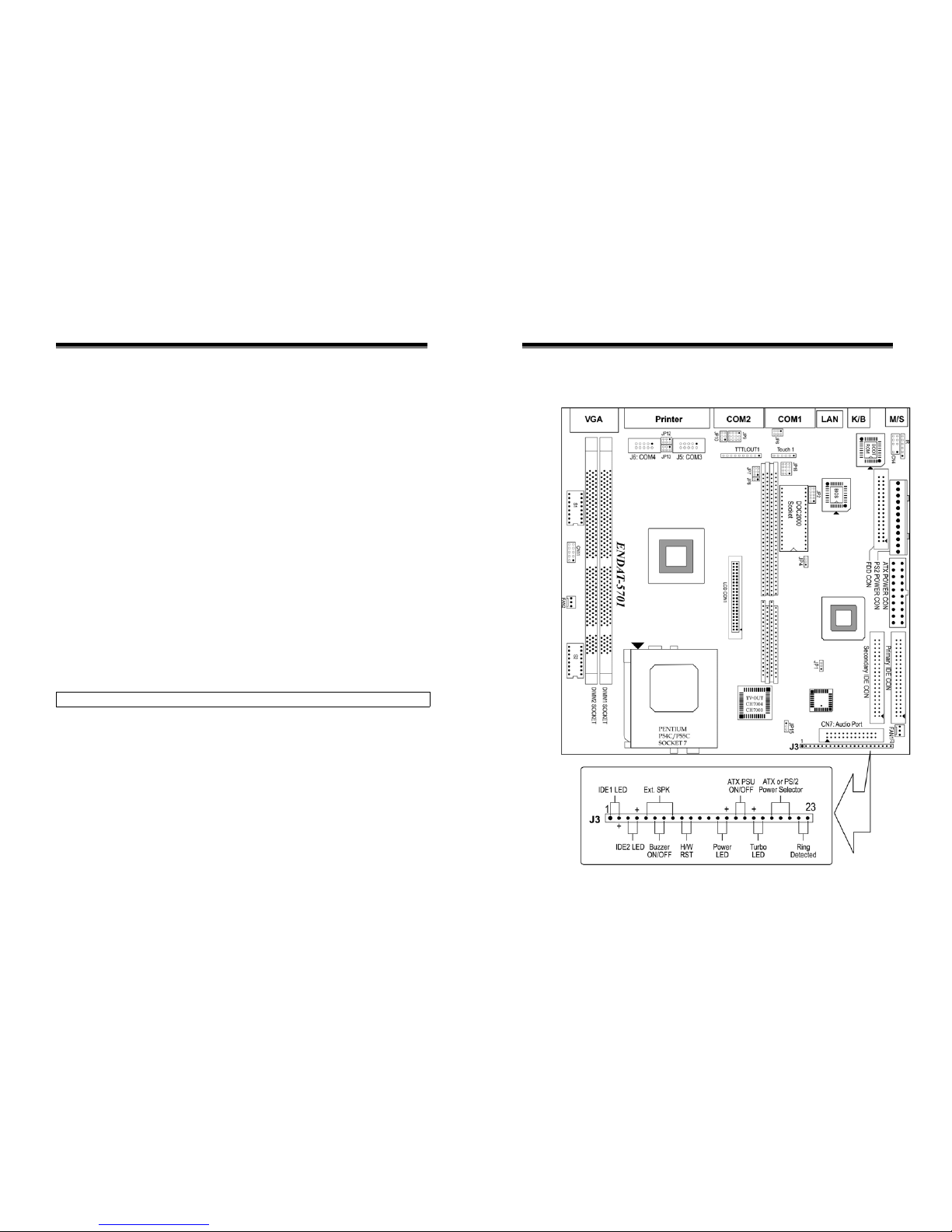
2-1. Jumpers and Connectors (ENDAT-5701)
Jumpers/Connectors Overview:
Function Jumpers/Connectors
CPU: CPU Clock Frequency Switch 1 (S1: SW1-SW4)
CPU Vcore Voltage Switch 2 (S2: SW1-SW5)
CPU Ratio Switch 2 (S2: SW6-SW8)
Connector for Cooling Fan FAN1,FAN2
Power Supply: Type (ATX or PS/2) CN2(ATX);CN1(PS/2)
Power Good JP15
ATX or PS/2 Power Selector J3 Pin 19, 20, 21
ATX Power On/Off Switch J3 Pin 15, 16
Audio /TV-Out Output Port Connector CN7
LAN Adapter Disable/Enable JP4
PCI INT selector for Expansion Slot JP16
COM3 Port J5
COM4 Port J6
COM3/COM4 IRQ Setting BIOS Defined
COM Ports Power Selector (COM1, 3,4) JP6, JP12, JP13
8
ENDAT-5701 and ENDAT-5901 All-In-One motherboard uses
Function Jumpers/Connectors
RS232/RS422/RS485 Selector (COM2) JP7, JP8, JP9, JP10
TTL Output Pin Header (For COM2) TTLOut1
Touch Panel Pin Header Touch1
DiskOnChip Memory Address JP2
LCD Connector LCD_CON1
Clear CMOS JP1
PS/2 Keyboard Jack CN6
PS/2 Mouse Jack CN2
PS/2 Mouse/KB Pin Header CN4
IR IR1
USB Header CN11
FDD Connector CN5
IDE 1 J1
IDE 2 J2
Header for Case Panel J3
IDE 1 LED J3 Pin 1, Pin 2
IDE 2 LED J3 Pin 3, Pin 4
External Speaker J3 Pin 5, Pin 8
Buzzer On/Off J3 Pin 6, Pin 7
Hardware Reset Switch J3 Pin 9, Pin 10
Power LED J3 Pin 13, Pin 14
ATX Power Supply On/Off Switch J3 Pin 15, Pin 16
Turbo LED for Case (for case only, no function) J3 Pin 17, Pin 18
ATX or PS/2 Power Selector J3 Pin 19, Pin 20, Pin 21
Ring-Detected J3 Pin 22, Pin 23
Note:
The cooling fan and heat sink are required for Pentium processors. Please pay
close attention to the direction of the CPU and cooling fan when install. Position
the cooling ventilator directly facing the regulator heat sink, which is located
beside the CPU socket. This will reduce the overheating of the regulator and
increase the reliability of the system.
User’s Manual
9
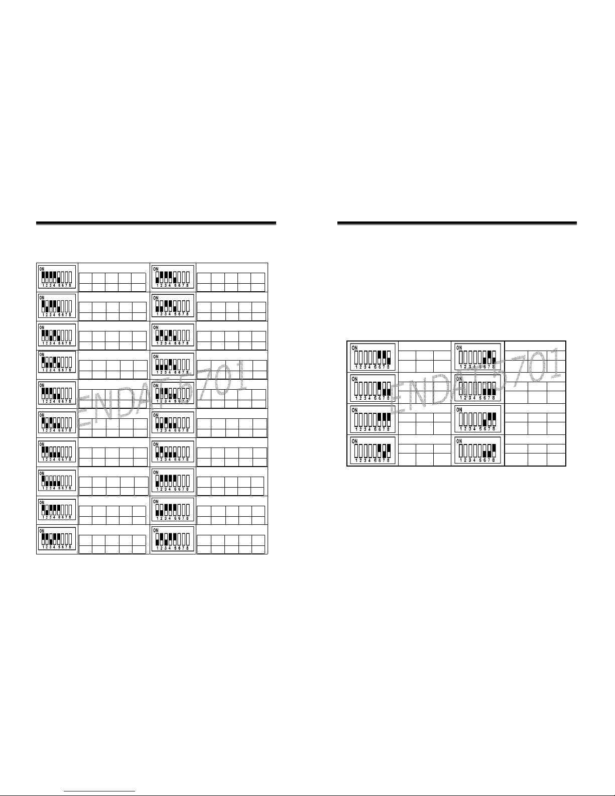
ENDAT-5701 CPU Vcore Setting: Switch2 (S2: SW1-SW5)
VCORE=3.5V
S1 S2 S3 S4 S5
ON ON ON ON OFF
VCORE=3.4V
S1 S2 S3 S4 S5
OFF ON ON ON OFF
VCORE=3.3V
S1 S2 S3 S4 S5
ON OFF ON ON OFF
VCORE=3.2V
S1 S2 S3 S4 S5
OFF OFF ON ON OFF
VCORE=3.1V
S1 S2 S3 S4 S5
ON ON OFF ON OFF
VCORE=3.0V
S1 S2 S3 S4 S5
OFF ON OFF ON OFF
VCORE=2.9V
S1 S2 S3 S4 S5
ON OFF OFF ON OFF
VCORE=2.8V
S1 S2 S3 S4 S5
OFF OFF OFF ON OFF
VCORE=2.7V
S1 S2 S3 S4 S5
ON ON ON OFF OFF
VCORE=2.6V
S1 S2 S3 S4 S5
OFF ON ON OFF OFF
VCORE=2.5V
S1 S2 S3 S4 S5
ON OFF ON OFF OFF
VCORE=2.4V
S1 S2 S3 S4 S5
OFF OFF ON OFF OFF
VCORE=2.3V
S1 S2 S3 S4 S5
ON ON OFF OFF OFF
VCORE=2.2V
S1 S2 S3 S4 S5
OFF ON OFF OFF OFF
VCORE=2.1V
S1 S2 S3 S4 S5
ON OFF OFF OFF OFF
VCORE=2.0V
S1 S2 S3 S4 S5
OFF ON ON ON ON
VCORE=1.95V
S1 S2 S3 S4 S5
ON OFF ON ON ON
VCORE=1.90V
S1 S2 S3 S4 S5
OFF OFF ON ON ON
VCORE=1.85V
S1 S2 S3 S4 S5
ON ON OFF ON ON
VCORE=1.80V
S1 S2 S3 S4 S5
OFF ON OFF ON ON
☛ Please make sure the CPU Vcore voltage and setting as mention
10
ENDAT-5701 and ENDAT-5901 All-In-One motherboard uses
above for your system. The wrong setting may cause system damaged
the CPU or system not working.
For ENDAT-5901 Rev.1D or later.
For ENDAT-5701 Rev.1F or later.
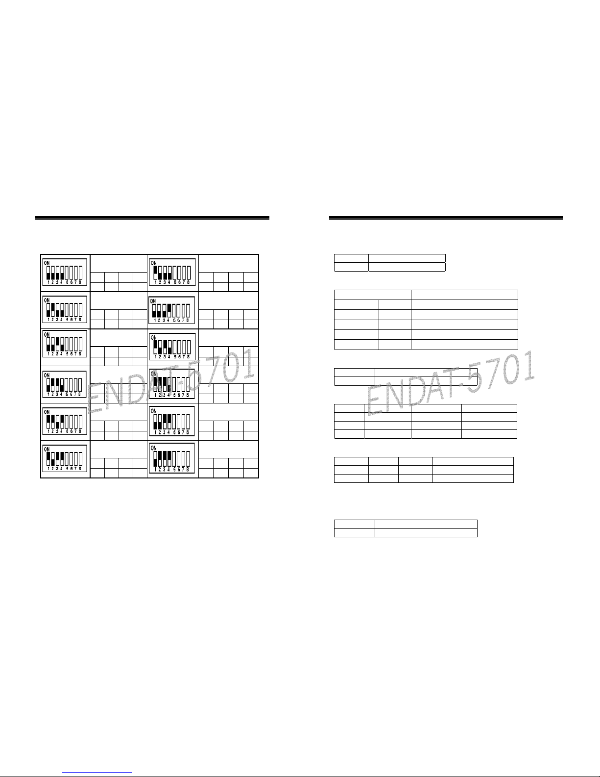
ENDAT-5701 CPU Ratio Setting: Switch2(S2:SW6-SW8)
S2 = 2.5x S2 = 3.0x
6 7 8 6 7 8
ON ON OFF
OFF ON OFF
S2 = 2.0x / 6.0x S2 = 1.5x / 3.5x
6 7 8 6 7 8
ON OFF OFF
OFF OFF OFF
S2 = 4.5x S2 = 5.0x
6 7 8 6 7 8
ON ON ON
OFF ON ON
S2 = 4.0x S2 = 5.5x
6 7 8 6 7 8
ON OFF ON
OFF OFF ON
☛ Please make sure the CPU Ratio and setting is followed as mention
above for your system. The wrong setting may cause the system not
working
User’s Manual
11
ENDAT-5701 CPU CLOCK Setting: Switch1(S1:SW1-SW4)
CPU = 60MHz
PCI CLK=30MHz
CPU = 66.8MHz
PCI CLK=33.4MHz
1 2 3 4 1 2 3 4
OFF OFF OFF OFF
ON OFF OFF OFF
CPU = 68.5MHz
PCI CLK=35MHz
CPU = 75MHz
PCI CLK=37.5MHz
1 2 3 4 1 2 3 4
OFF ON OFF OFF
OFF OFF OFF ON
CPU = 97MHz
PCI LK=26.67MHz
CPU = 83.3MHz
PCICLK=27.76MHz
1 2 3 4 1 2 3 4
OFF OFF ON OFF
ON OFF ON OFF
CPU = 95.25MHz
PCI LK=31.75MHz
CPU = 100MHz
PCI CLK=33.33MHz
1 2 3 4 1 2 3 4
OFF ON ON OFF
ON ON ON OFF
CPU = 105MHz
PCI CLK=35MHz
CPU = 110MHz
PCI CLK=36.67MHz
1 2 3 4 1 2 3 4
ON ON OFF ON
OFF OFF ON ON
CPU = 115MHz
PCI CLK=38.33MHz
CPU = 120MHz
PCI CLK=40MHz
1 2 3 4 1 2 3 4
ON OFF ON ON
OFF ON ON ON
☛ Please make sure the CPU Clock and setting is followed as mention
above for your system. The wrong setting may cause the system not
working.
12
ENDAT-5701 and ENDAT-5901 All-In-One motherboard uses
JP1: CMOS Data Clear:
Pin 1-2 *
Normal
Pin 2-3
Clear CMOS Data
JP2: DiskOnChip Memory Address Selector
JP2 Memory Address
1-2 7-8
0C800H-0C9FFH
1-2 9-10
0CC00H-0CDFFH
3-4 7-8
0DCCCH-0D1FFH
3-4 9-10
0D400H-0D5FFH
5-6 7-8
0D800H-0D9FFH(Default)
JP4: On-board LAN Disable/Enable
Pin 1-2 *
Enable On-Board LAN
Pin 2-3
Disable On-Board LAN
JP6 (COM1) / JP12 (COM3) / JP13 (COM4) Voltage Selector:
Pin No. JP6(COM1) JP12(COM3) JP13(COM4)
1-2 +5V +12V +12V
*3-4 STD RS-232 STD RS-232 STD..RS-232
5-6 +12V +5V +5V
JP7, JP8, JP9: RS232 / 485 Selector for COM2
TYPE JP7 JP8 JP9
RS-232 * 1-2 Open 1-2, 4-5, 7-8, 10-11
RS-485 3-4 Close 2-3, 5-6, 8-9, 11-12
∗
Make sure the port mode is set up correctly before installing any
peripherals.
JP15: On-board Power Good Selector
Pin 1-2 *
Using External Power Good
Pin 2-3
Using On Board Power Good
User’s Manual
13
JP16: On-board Expansion SLOT INT Selector
INT Routing JP16
A, B, C, D
1-2, 4-5, 7-8, 10-11
B, C, D, A
2-3, 5-6, 8-9, 11-12
AN1, FAN2: CPU / 2nd Cooling Fan Connector
Pin No. Function
Pin 1
Sensor Pin.
Pin 2
+12V
Pin 3
GND
J3’s Pin15;16;19;20;21: For ATX Power Supply
Close Pin 19-20
Using PS/2 AT Power Supply
Close Pin 20-21
Using ATX Power Supply
Pin 15; Pin 16
On/Off Switch for ATX Power
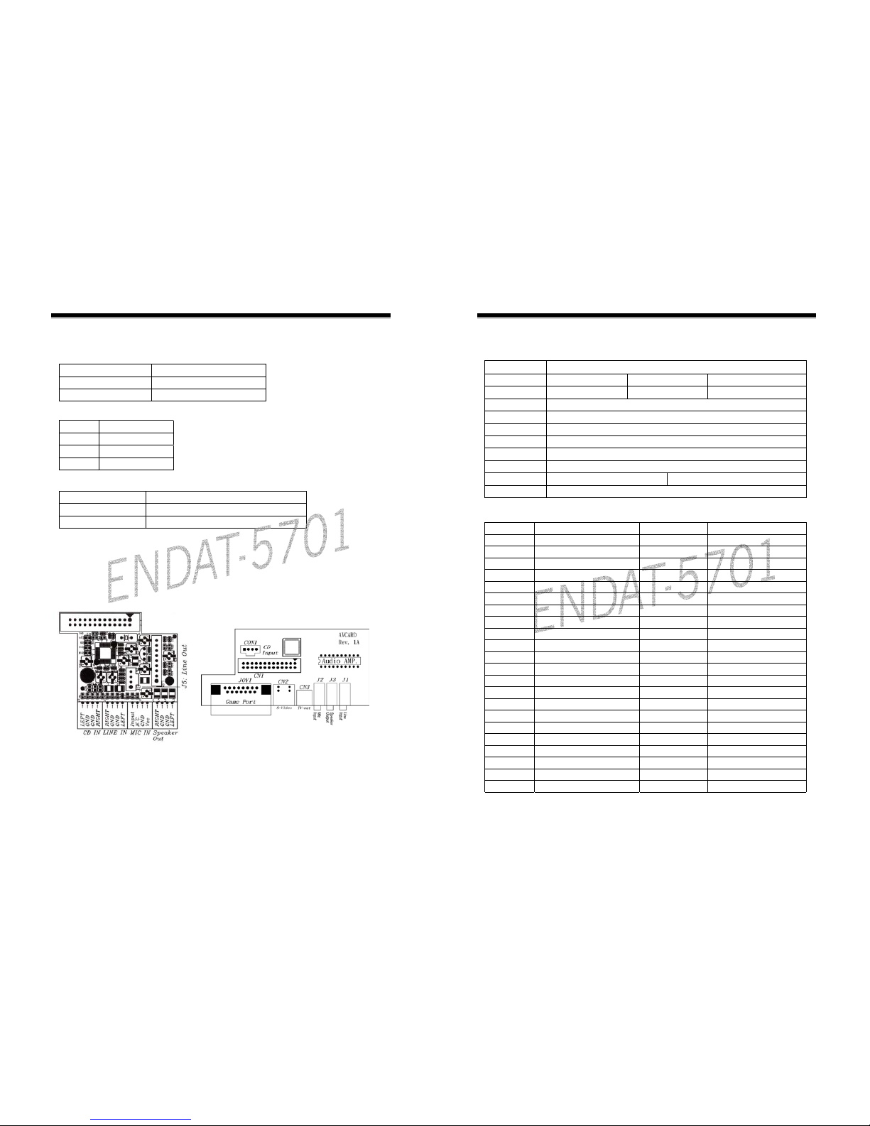
CN7: Audio Output Port connector via AV Card Kit (Optional)
The AV Card Kit Adapter supports Sound, TV-OUT, S-Video and Game
Port. Please close pin13-14 to disable onboard Audio features if the AV
Card Kit is not inserted onto the CN7 connector.
UC-A001 AV Card
14
ENDAT-5701 and ENDAT-5901 All-In-One motherboard uses
J3: Case Panel connection
Pin No. Description
1, 2 IDE 1 LED Pin 1 = - Pin 2 = +
3, 4 IDE 2 LED Pin 3 = - Pin 4 = +
5, 8 External Speaker
6, 7 Onboard Buzzer
9, 10 Reset Switch
13,14 Power LED Indicator
15, 16 Power On/Off Switch (for ATX Power only)
17, 18 Turbo LED(for case only, no function)
19, 20, 21 19-20 for AT Power 20-21 for ATX Power
22, 23 Modem Ring Detected / Wake on LAN
LCD_CON1 (Only for Support LCD Version)
Pin No. Description Pin No. Description
1 VBL 2 VBL
3 GND 4 GND
5 VDDLCD(+3.3V) 6 VDDLCD(+3.3V)
7 ENPVEE 8 GND
9 FPD23 10 FPD22
11 FPD17 12 FPD16
13 FPD11 14 FPD10
15 FPD9 16 FPD8
17 FPD21 18 FPD20
19 FPD15 20 FPD14
21 FDP7 22 FPD6
23 FPD5 24 FPD4
25 FPD19 26 FPD 18
27 FPD13 28 FPD12
29 FPD3 30 FPD2
31 FPD1 32 FPD0
33 GND 34 GND
35 SHFCLK 36 FLM
37 M_DE 38 LP
39 GND 40 VCCUPBKL
41 VCCUPBKL 42 KEY.
43 VDDLCD(+5V) 44 VDDLCD(+5V)
*Please make sure the Pin 1 location before inserting the LCD connector.
User’s Manual
15
18Bit TFT DSTN / 16Bit DSTN LCD Panel Mapping
18Bit
TFT
16Bit
DSTN
18Bit / 18+18
TFT
Pin No.
NC N.C. FPD23 9
NC N.C FPD22 10
NC N.C FPD21 17
NC N.C. FPD20 18
NC N.C FPD19 25
NC N.C FPD18 26
B0 N.C FPD17 11
B1 N.C FPD16 12
G0 UD7 FPD15 19
G1 UD6 FPD14 20
R0 UD5 FPD13 27
R1 UD4 FPD12 28
B2 UD3 FPD11 13
B3 UD2 FPD10 14
B4 UD1 FPD9 15
B5 UD0 FPD8 16
G2 LD7 FPD7 21
G3 LD6 FPD6 22
G4 LD5 FPD5 23
G5 LD4 FPD4 24
R2 LD3 FPD3 29
R3 LD2 FPD2 30
R4 LD1 FPD1 31
R5 LD0 FPD0 32
16
ENDAT-5701 and ENDAT-5901 All-In-One motherboard uses
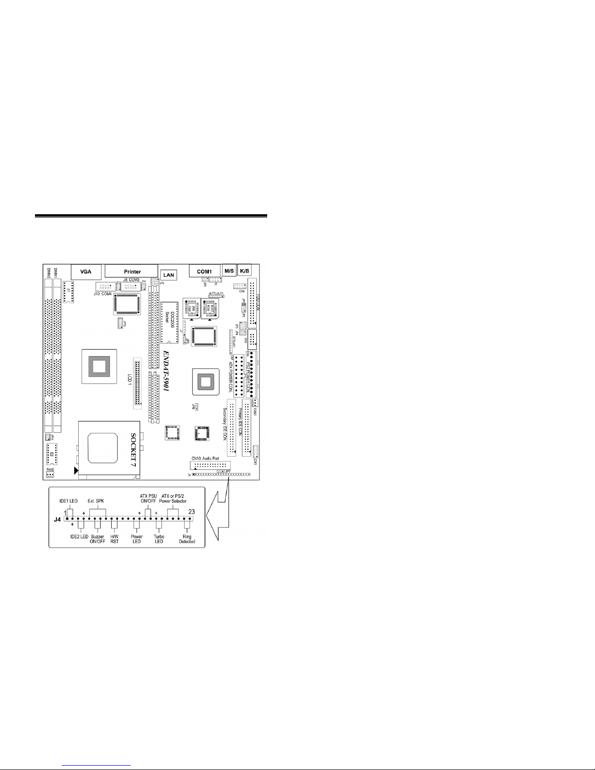
2-2. Jumpers and Connectors (ENDAT-5901)
Function Jumpers/Connectors
CPU: CPU Clock Frequency Switch 1 (S1: SW1-SW4)
CPU Ratio Switch 2 (S2: SW6-SW8)
CPU Vcore Voltage Switch 2 (S2: SW1-SW5)
Connector for Cooling Fan FAN1; FAN2
Power Supply: Type (ATX or PS/2) CN7(ATX) ; CN4(PS/2)
Power Good JP7
ATX or PS/2 Power Selector J4 Pin 19, Pin 20, Pin 21
ATX Power on/off Switch J4 Pin 15, Pin 16
Audio/TV-Out Output Port Connector CN10
Touch Panel Pin Header J6
LCD Connector LCD_CON1
TTL Output Pin Header J2
LAN Adapter Disable/Enable JP8
COM2/COM3/COM4 CN3, J8, J10
PCI INT selector for Expansion Slot JP9
COM Ports Power Selector(COM1/3/4) JP5, JP11, JP13
COM3/COM4 IRQ Setting BIOS Defined
RS232/RS422/RS485 Selector JP1, JP2, JP3,JP4
DiskOnChip Memory Address JP12
Clear CMOS JP6
PS/2 Keyboard Header CN6 : PIN 1-3-5-7
PS/2 Mouse Header CN6 : PIN 2-4-6-8
IR J7
USB Header CN1
IDE 1 Connector J1
 Loading...