

Page 1
UK-electronic ©2012/15
Manual for the Kit Zentaurus Rev 1.21 with buffer
or True bypass
Page 1..............................................Cover
Page 2..3..........................................Allocations, basics
Page 4...5.........................................Bill of material
Page 6...7.........................................Soldering the pcb
Page 8…..........................................Building
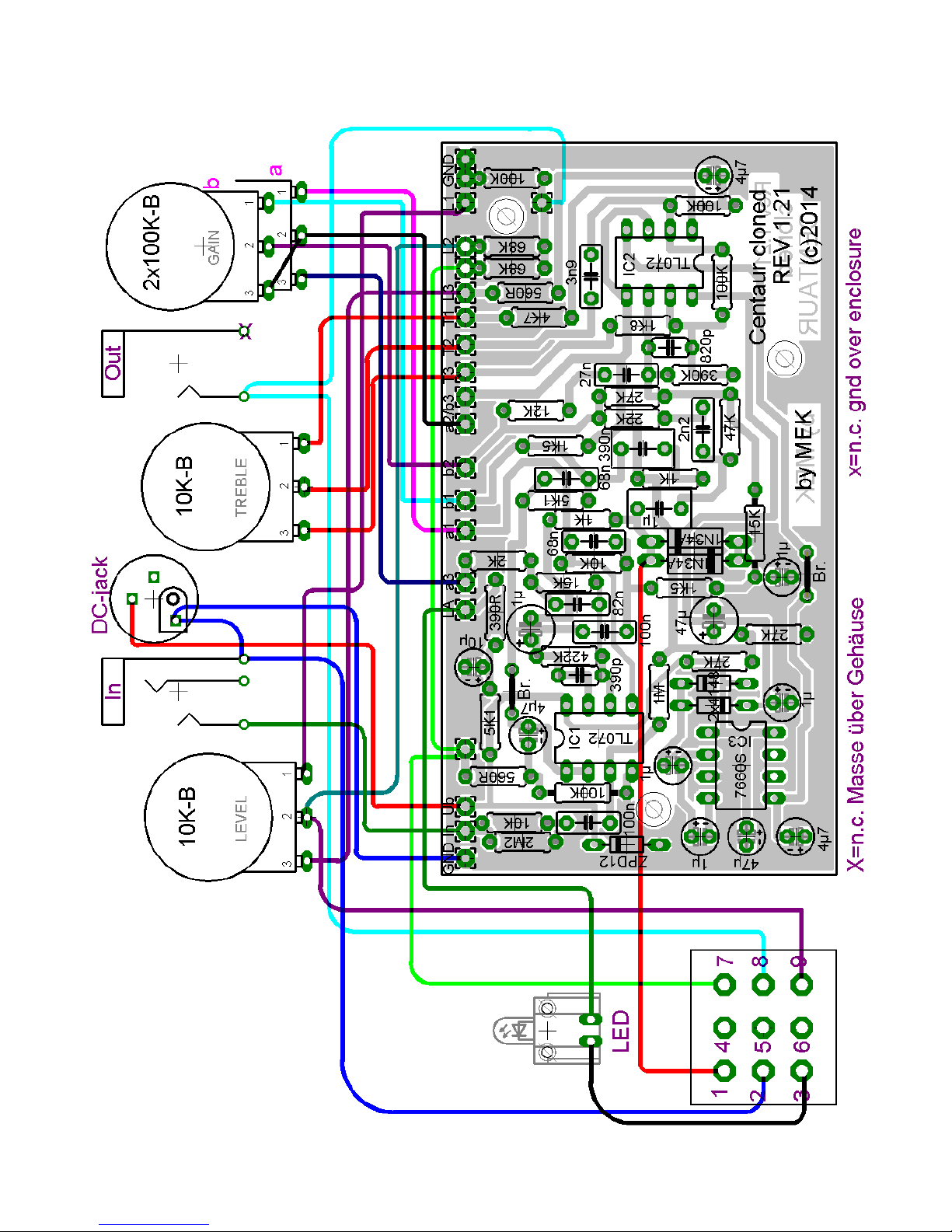
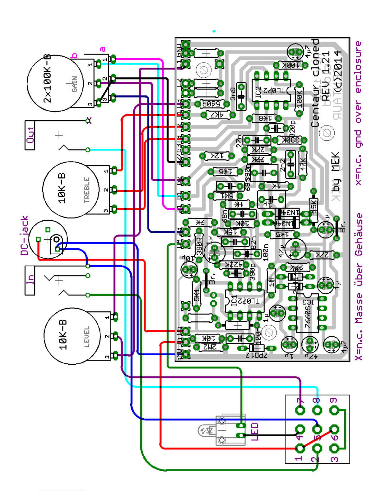
Page 9..............................................Wiring TB
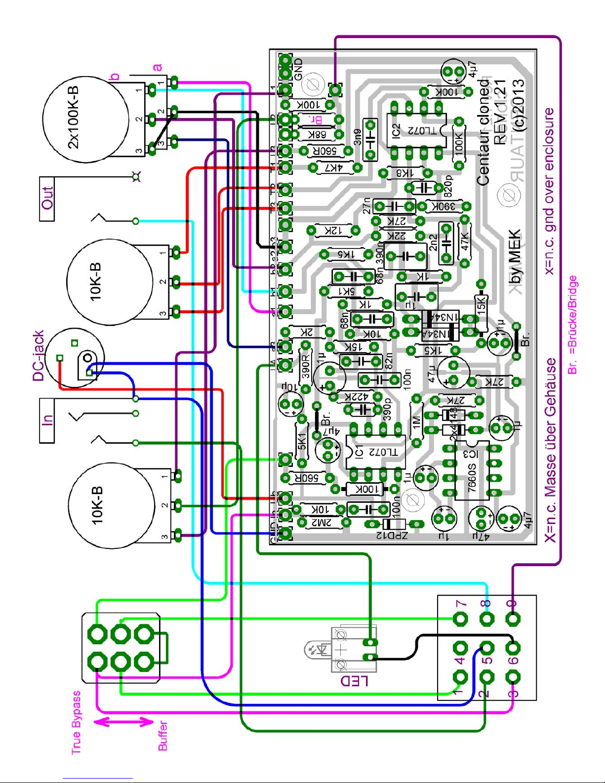
Page 10............................................Wiring with buffer
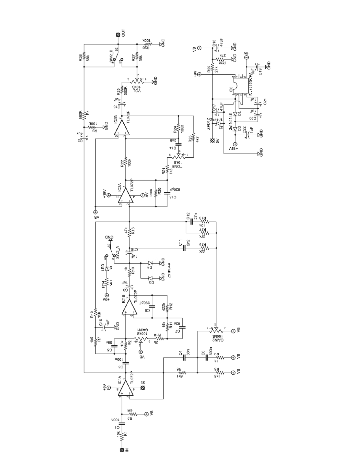
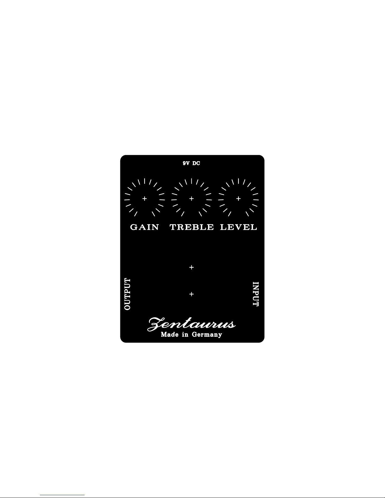
Page 11...20....................................drill template, foil template, circuit diagram
Please download the manual at the store. Thank’s!
2009/13 © UK-electronic
Page 2
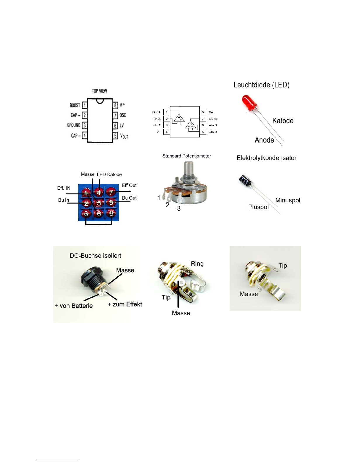
Important connections of some components
ICL7660SCPA
TL 072
3PDT
2009/13 © UK-electronic
Page 3
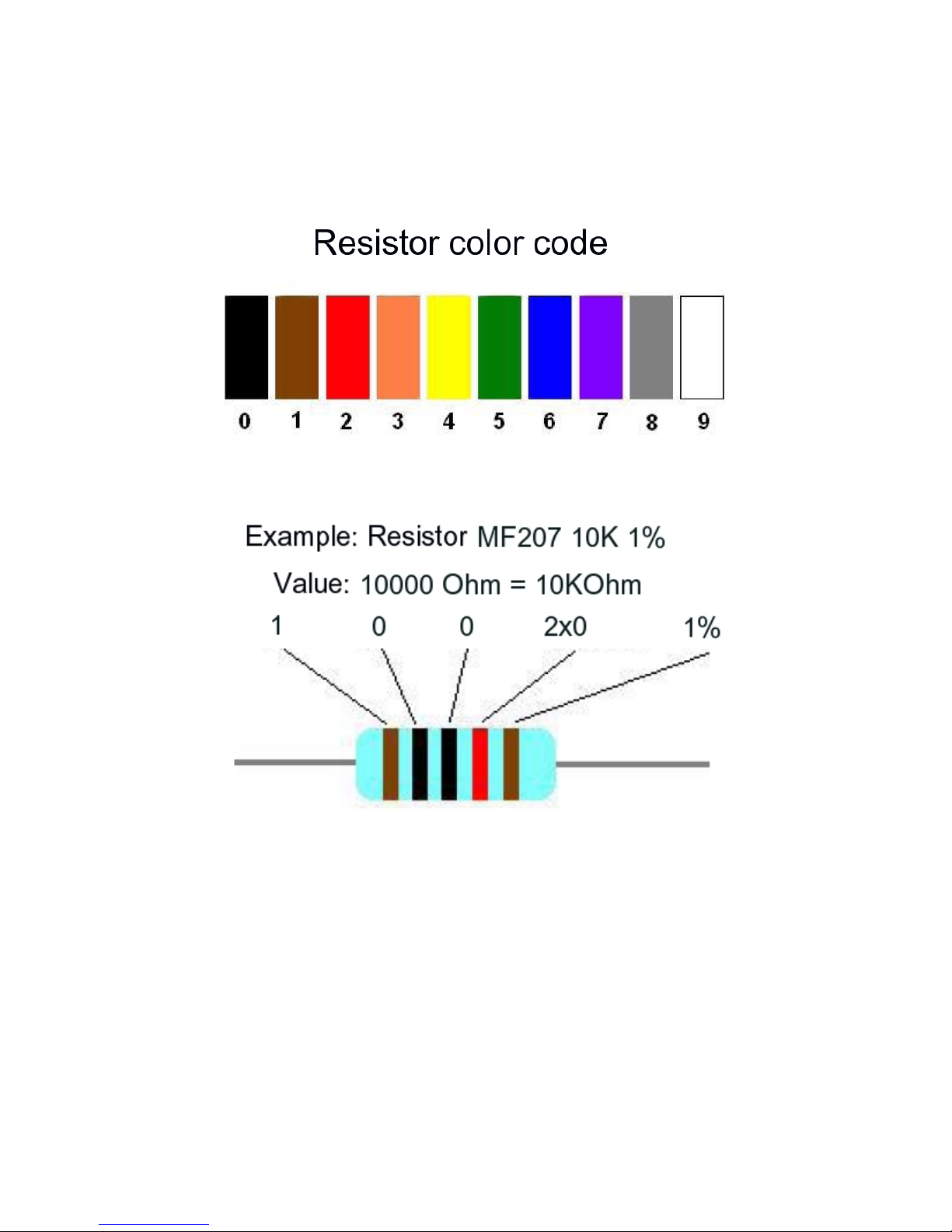
Color table for resistors MF207 FTE52 1% and a example
Page 4
Bill of material
Quantity Description
resistor
1 Resistor 390R (orange/white/black/black/brown)
2 Resistor 560R (green/blue/black/black/brown)
2 Resistor 1K (brown/black/black/brown/brown)
2 Resistor 1K5 (brown/green/black/brown/brown)
1 Resistor 1K8 (brown/grey/black/brown/brown)
1 Resistor 2K (red/black/black/brown/brown)
1 Resistor 4K7 (yellow/violet/black/brown/brown)
2 Resistor 5K1 (green/brown/black/brown/brown)
2 Resistor 10K (brown/black/black/red/brown)
1 Resistor 12K (brown/red/black/red/brown)
2 Resistor 15K (brown/green/black/red/brown)
1 Resistor 22K (red/red/black/red/brown)
3 Resistor 27K (red/violet/black/red/brown)
1 Resistor 47K (yellow/violet/black/red/brown)
2 Resistor 68K (blue/grey/black/red/brown)
4 Resistor 100K (brown/black/black/orange/brown)
1 Resistor 390K (orange/white/black/orange/brown)
1 Resistor 422K (yellow/red/red/orange/brown)
1 Resistor 1M (brown/black/black/yellow/brown)
1 Resistor 2M2 (red/red/black/yellow/brown)
capacitors
1 Capacitor ceramic 390pF (391)
1 Capacitor ceramic 820pF (821)
1 Capacitor MKT 3n9 (0.0039µF) 392
1 Capacitor MKT 2n2 (0.0022µF) 222
1 Capacitor MKT 27nF (0.027µF) 273
2 Capacitor MKT 68nF (0.068µF) 683
1 Capacitor MKT 82nF (0.082µF) 823
2 Capacitor MKT 100nF (0.1µF) 104
1 Capacitor MKT 390nF (0.39µF) 394
1 Capacitor MKT 1µF - 105
5 Electrolytic RASM 1µF/50V
Page 5

3 Electrolytic RASM 4,7µF/50V
1 Electrolytic RASM 10µF/50V
2 Electrolytic RASM 47µF/25V
Diodes
1 Z-Diode 12V – ZPD12 – Cathode line
2 Si-Diode 1N4148 – Cathode li ne
2 Ge-Diode 1N34A/ OA90/ AA119 or other – Ca th o de line
1 LED 3mm blue
semiconductors
1 ICL 7660 SCPA (DC-DC pump charge)
2 TL072 CN oder CP
Potentiometer
1 Dual potentiometer 2x100K-B (linear)
2 Potentiometer 10K-B (linear)
Mechanical
1 Mono jack 6,35mm
1 Stereo jack 6,35mm
1 3PDT Switch
1 DC-jack isolated (5,5/2,1)
2 washer 10.4mm (Audio jacks)
3 Washer 7,4mm (Potentiometer)
1 Battery connector
3 Adhesive self spacer 12,7mm
1 LED bezel crome f. 3mm outer reflector
1 Some coloured wire
1 PCB Zentaurus REV 1.21.
3 Cable fastener
2009/13 © UK-electronic
Page 6
Soldering the pcb
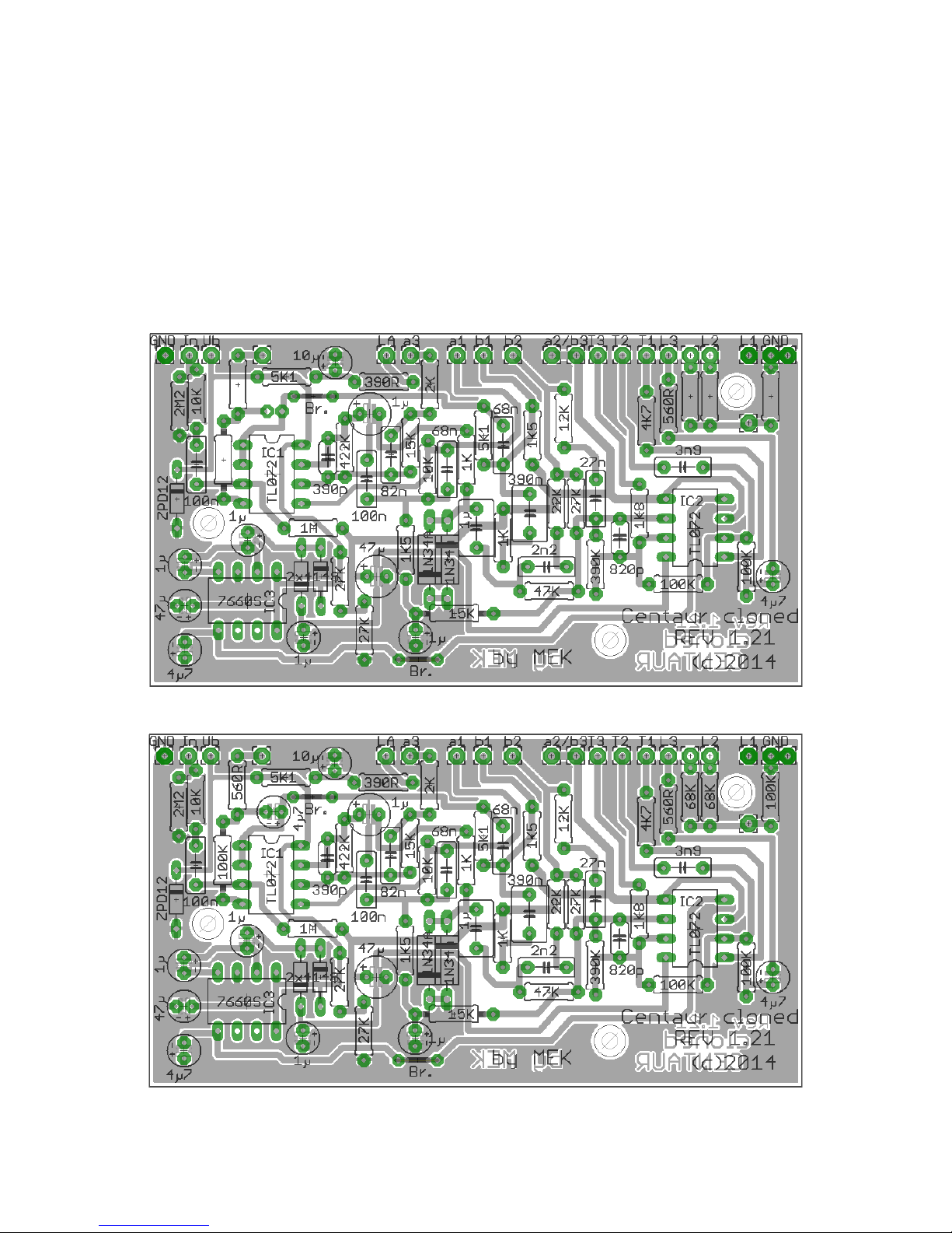
First, the printed circuit board is assembled by means of the placement schedule shown below.
You should decide at the outset whether t he B uffered or True Bypass version is built. In the true
bypass version of the unlabeled components need not be loaded (loading images in the
description)! For this we should start with the lowest components to be fitted, ie first the 2
bridges (Br), resistors, diodes, IC sockets, capacitors. Then the circuits are used at the end. Clean
work, especially the execution of the solder joints should have top priority to generally be
eliminated in order to save a painstaking troubleshooting from the outset assembly and solder
defects.
Layout for True Bypass
Layout for buffered version
2009/13 © UK-electronic
Page 7
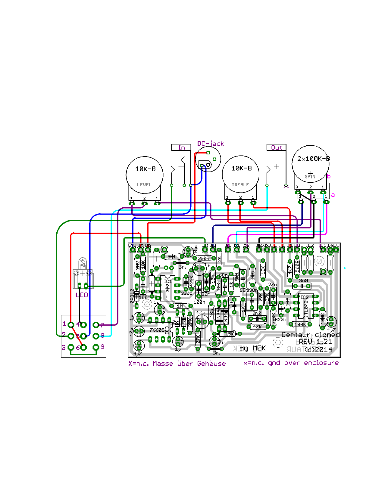
After the PCB is fully soldered to cut several wires from approx. 10 to 15 cm le ng th and solder
them into the points of the circuit board to which the potentiometers come from below. Next up is
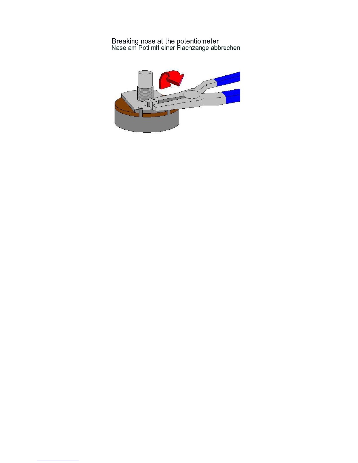
the enclosure that it has drilled before accordingly with the mechanical components (6.3 mm
jacks, 3PDT switch, potentiometer-[the (guide tabs) to easily breaking the potentiometers with
pliers from Æ see the picture.], DC jack and the bezel for the LED equipped.)
The wires for the power supply (red an d b lue), as well as the output signal of lug 2 of th e level
pots, are already pre-wired.
Wiring for True Bypass
2009/13 © UK-electronic
Page 8
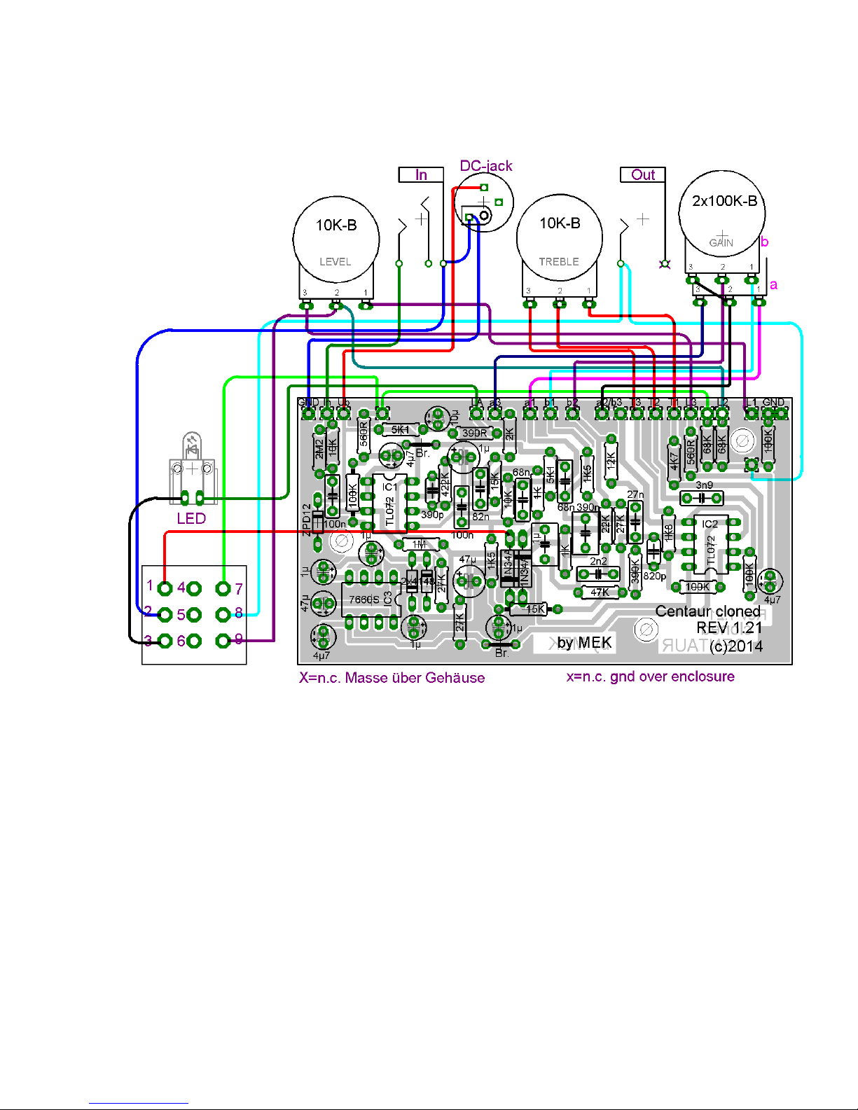
Wiring the buffered version
The two green wires in the wiring diagram is soldered directly under the circuit board at
the marked points.!
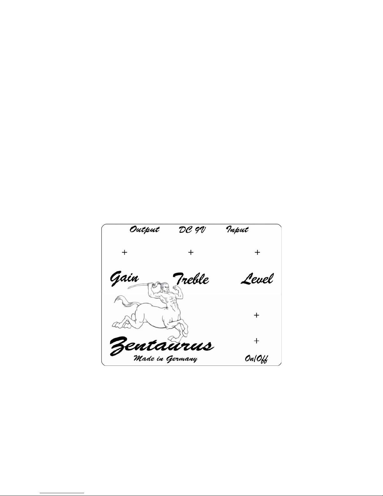
At the appenidix you found templates for a drilling and a templete for a foil for the enclosure.
When printing the PDF files, the printer must set to "No adjustment" otherwise the print is not
true to size
Finally, only the remaining connections are soldered displayed schema from the switch to the
PCB according to the above. To do this turn the circuit board on the compon ent side. To solder
the Green wires in the wiring diagram, (buffered version), from the bottom of the circ uit b oa rd
where the both 68 k and 100 k resistance are connected, as well as the two GE diodes.
2009/13 © UK-electronic
Page 9
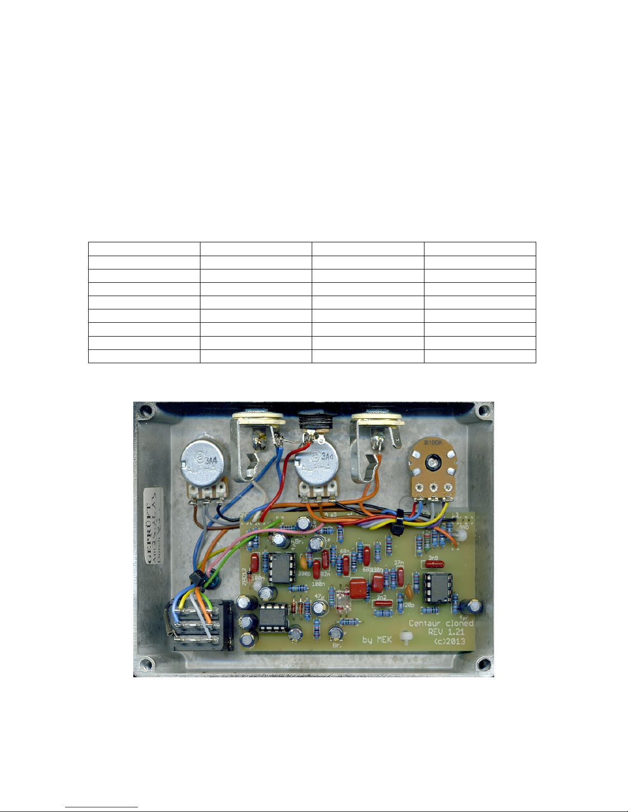
As enclosure choose Hammond 1590BB or GEH 090.
Drilling diameters:
Audio jacks: 9.3mm
DC-jack. 12mm
3PDT switch: 12mm
LED Bezel : 6mm
Have fun, the team of UK-e le ctronic!
Voltage chart: Power supply 9V DC , measured again GND!!
Pin IC3 7660S IC1 TL072 IC2 TL072
1
9.00V 4.5V 4.5V
2
4.48V 4.5V 4.5V
3
0.6V 4.00V 4.5V
4
-4.14V 0V -8.38V
5
-8.39V 4.5V 4.5V
6
4.39V 4.5V 4.5V
7
6.94V 4.5V 4.5V
8
9.00V 9.00V 16.85V
Zentaurus PCB 2013 (at the new pcb, the 100K resistor is right from the adehesive spacer!
2009/15 © UK-electronic
Page 10
Page 11
Page 12
Page 13

+++
+
+
Zentaurus
Gain
Treble
Level
Made in Germany
Output
DC 9V
Input
On/Off
Page 14
Page 15
 Loading...