

Page 1

Abstract
This document describes the features and the system integration of
TOBY-L1 series LTE wireless modules.
These modules are a complete and cost efficient 4G solution offering
100 Mb/s download, 50 Mb/s upload, and covering up to 3 LTE Bands
in the compact TOBY form factor.
www.u-blox.com
35.6 x 24.8 x 2.6 mm
locate, communicate, accelerate
TOBY-L1 series
LTE modules
System Integration Manual
Page 2

TOBY-L1 series - System Integration Manual
Document Information
Title
TOBY-L1 series
Subtitle
LTE modules
Document type
System Integration Manual
Document number
UBX-13001482
Document status
Objective Information
Document status information
Objective
Specification
This document contains target values. Revised and supplementary data will be published
later.
Advance
Information
This document contains data based on early testing. Revised and supplementary data will
be published later.
Preliminary
This document contains data from product verification. Revised and supplementary data
may be published later.
Released
This document contains the final product specification.
Name
Type number
Firmware version
PCN / IN
TOBY-L100
TOBY-L100-00S-00
G0.V.00.00.08
TOBY-L110
TOBY-L110-00S-00
G0.EE.00.00.08
This document and the use of any information contained therein, is subject to the acceptance of the u-blox terms and conditions. They
can be downloaded from www.u-blox.com.
u-blox makes no warranties based on the accuracy or completeness of the contents of this document and reserves the right to make
changes to specifications and product descriptions at any time without notice.
u-blox reserves all rights to this document and the information contained herein. Reproduction, use or disclosure to third parties without
express permission is strictly prohibited. Copyright © 2013, u-blox AG.
u-blox® is a registered trademark of u-blox Holding AG in the EU and other countries.
This document applies to the following products:
Trademark Notice
Microsoft and Windows are either registered trademarks or trademarks of Microsoft Corporation in the United States and/or other countries.
All other registered trademarks or trademarks mentioned in this document are property of their respective owners.
UBX-13001482 Objective Information
Page 2 of 85
Page 3

TOBY-L1 series - System Integration Manual
Preface
u-blox Technical Documentation
As part of our commitment to customer support, u-blox maintains an extensive volume of technical
documentation for our products. In addition to our product-specific technical data sheets, the following manuals
are available to assist u-blox customers in product design and development.
AT Commands Manual: This document provides the description of the supported AT commands by the
TOBY-L1 series modules to verify all implemented functionalities.
System Integration Manual: This manual provides hardware design instructions and information on how to
set up production and final product tests.
Application Note: document provides general design instructions and information that applies to all u-blox
Wireless modules. See Related documents section for a list of Application Notes related to your Wireless
Module.
How to use this Manual
The TOBY-L1 series System Integration Manual provides the necessary information to successfully design and
configure the u-blox wireless modules.
This manual has a modular structure. It is not necessary to read it from the beginning to the end.
The following symbols are used to highlight important information within the manual:
An index finger points out key information pertaining to module integration and performance.
A warning symbol indicates actions that could negatively impact or damage the module.
Questions
If you have any questions about u-blox Wireless Integration:
Read this manual carefully.
Contact our information service on the homepage http://www.u-blox.com
Read the questions and answers on our FAQ database on the homepage http://www.u-blox.com
Technical Support
Worldwide Web
Our website (www.u-blox.com) is a rich pool of information. Product information, technical documents and
helpful FAQ can be accessed 24h a day.
By E-mail
Contact the closest Technical Support office by email. Use our service pool email addresses rather than any
personal email address of our staff. This makes sure that your request is processed as soon as possible. You will
find the contact details at the end of the document.
Helpful Information when Contacting Technical Support
When contacting Technical Support, have the following information ready:
Module type (e.g. TOBY-L100) and firmware version
Module configuration
Clear description of your question or the problem
A short description of the application
Your complete contact details
UBX-13001482 Objective Information Preface
Page 3 of 85
Page 4

TOBY-L1 series - System Integration Manual
Contents
Preface ................................................................................................................................ 3
Contents .............................................................................................................................. 4
1 System description ....................................................................................................... 7
1.1 Overview .............................................................................................................................................. 7
1.2 Architecture .......................................................................................................................................... 9
1.2.1 Internal blocks ............................................................................................................................. 10
1.3 Pin-out ............................................................................................................................................... 11
1.4 Operating modes ................................................................................................................................ 13
1.5 Supply interfaces ................................................................................................................................ 15
1.5.1 Module supply input (VCC) ......................................................................................................... 15
1.5.2 2.5v supply output (V_BCKP) ....................................................................................................... 19
1.5.3 1.8v supply output (V_INT) .......................................................................................................... 19
1.6 System function interfaces .................................................................................................................. 20
1.6.1 Module power-on ....................................................................................................................... 20
1.6.2 Module power-off ....................................................................................................................... 21
1.6.3 Module reset ............................................................................................................................... 21
1.7 Antenna interface ............................................................................................................................... 23
1.7.1 Antenna RF interfaces (ANT1 / ANT2) ......................................................................................... 23
1.8 SIM interface ...................................................................................................................................... 23
1.8.1 SIM card interface ....................................................................................................................... 23
1.8.2 SIM card detection ...................................................................................................................... 23
1.9 Serial interfaces .................................................................................................................................. 25
1.9.1 USB ............................................................................................................................................. 25
1.10 General Purpose Input/Output (GPIO) ............................................................................................. 27
1.11 Reserved pins (RSVD) ...................................................................................................................... 27
1.12 System features............................................................................................................................... 28
1.12.1 Network indication ...................................................................................................................... 28
1.12.2 TCP/IP and UDP/IP ....................................................................................................................... 29
1.12.3 FTP .............................................................................................................................................. 29
1.12.4 HTTP ........................................................................................................................................... 29
1.12.5 SMTP ........................................................................................................................................... 29
1.12.6 Firmware upgrade Over The Air (FOTA) ....................................................................................... 29
1.12.7 Power saving ............................................................................................................................... 29
2 Design-in ..................................................................................................................... 31
2.1 Supply interfaces ................................................................................................................................ 32
2.1.1 Module supply (VCC) .................................................................................................................. 32
2.1.2 2.5v supply (V_BCKP) .................................................................................................................. 40
2.1.3 1.8v supply (V_INT) ...................................................................................................................... 41
2.2 System functions interfaces ................................................................................................................ 42
UBX-13001482 Objective Information Contents
Page 4 of 85
Page 5

TOBY-L1 series - System Integration Manual
2.2.1 Module power-on (PWR_ON) ...................................................................................................... 42
2.2.2 Module reset (RESET_N) .............................................................................................................. 43
2.3 Antenna interface ............................................................................................................................... 45
2.3.1 Antenna RF interface (ANT) ......................................................................................................... 45
2.4 SIM interface ...................................................................................................................................... 50
2.5 Serial interfaces .................................................................................................................................. 54
2.5.1 USB interface............................................................................................................................... 54
2.6 General Purpose Input/Output (GPIO) ................................................................................................. 56
2.7 Reserved pins (RSVD) .......................................................................................................................... 57
2.8 Module placement.............................................................................................................................. 57
2.9 Module footprint and paste mask ....................................................................................................... 58
2.10 Thermal guidelines .......................................................................................................................... 60
2.11 ESD guidelines ................................................................................................................................ 62
2.11.1 ESD immunity test overview ........................................................................................................ 62
2.11.2 ESD immunity test of u-blox TOBY-L1 series reference designs .................................................... 62
2.11.3 ESD application circuits ................................................................................................................ 63
2.12 Schematic for TOBY-L1 series module integration ........................................................................... 65
2.13 Design-in checklist .......................................................................................................................... 67
2.13.1 Schematic checklist ..................................................................................................................... 67
2.13.2 Layout checklist ........................................................................................................................... 68
2.13.3 Antenna checklist ........................................................................................................................ 68
3 Handling and soldering ............................................................................................. 69
3.1 Packaging, shipping, storage and moisture preconditioning ............................................................... 69
3.2 Soldering ............................................................................................................................................ 69
3.2.1 Soldering paste............................................................................................................................ 69
3.2.2 Reflow soldering ......................................................................................................................... 69
3.2.3 Optical inspection ........................................................................................................................ 71
3.2.4 Cleaning ...................................................................................................................................... 71
3.2.5 Repeated reflow soldering ........................................................................................................... 71
3.2.6 Wave soldering............................................................................................................................ 71
3.2.7 Hand soldering ............................................................................................................................ 71
3.2.8 Rework ........................................................................................................................................ 71
3.2.9 Conformal coating ...................................................................................................................... 71
3.2.10 Casting ........................................................................................................................................ 72
3.2.11 Grounding metal covers .............................................................................................................. 72
3.2.12 Use of ultrasonic processes .......................................................................................................... 72
4 Approvals .................................................................................................................... 73
4.1 Product certification approval overview ............................................................................................... 73
4.2 Federal Communications Commission and Industry Canada notice ..................................................... 74
4.2.1 Safety Warnings review the structure .......................................................................................... 74
4.2.2 Declaration of Conformity – United States only ........................................................................... 74
4.2.3 Modifications .............................................................................................................................. 74
4.3 R&TTED and European Conformance CE mark ................................................................................... 76
UBX-13001482 Objective Information Contents
Page 5 of 85
Page 6

TOBY-L1 series - System Integration Manual
5 Product Testing........................................................................................................... 77
5.1 u-blox in-series production test ........................................................................................................... 77
5.2 Test parameters for OEM manufacturer .............................................................................................. 77
5.2.1 “Go/No go” tests for integrated devices ...................................................................................... 78
5.2.2 Functional tests providing RF operation ....................................................................................... 78
Appendix .......................................................................................................................... 80
A Glossary ...................................................................................................................... 81
Related documents........................................................................................................... 83
Revision history ................................................................................................................ 84
Contact .............................................................................................................................. 85
UBX-13001482 Objective Information Contents
Page 6 of 85
Page 7

TOBY-L1 series - System Integration Manual
Module
Region /
Operator
LTE
UMTS
GSM
GNSS
Interfaces
Audio
Features
TOBY-L100
Verizon
3
4, 13 1 6 • • TOBY-L110
Europe
3
3, 7, 20
1 6 • •
1 System description
1.1 Overview
The TOBY-L1 series comprises LTE-only modules in the very small LGA form-factor (35.6 x 24.8 x 2.6 mm) that
are easy to integrate in compact designs.
TOBY-L1 series wireless modules provide 4G LTE-only data communication supports up to three LTE-FDD bands:
TOBY-L100 is designed for operation on the LTE Verizon network in North America (LTE bands 4, 13), and
meets the requirements of Verizon network certification for LTE only devices.
TOBY-L110 is designed for operation on the LTE European networks (LTE bands 3, 7, 20), and meets the
requirements of European networks certification for LTE only devices.
LTE-only modules offer cost advantages compared to multi-mode (LTE/3G/2G) modules and are optimized for
applications using only LTE networks. Additionally, the TOBY-L1 series modules are form-factor compatible with
the popular u-blox wireless module families: this allows customers to take the maximum advantage of their
hardware and software investments, and provides very short time-to-market.
The modules are dedicated for data transfer, supporting a high-speed USB 2.0 interface. With LTE Category 3
data rates of 100 Mb/s (downlink) and 50 Mb/s (uplink), the modules are ideal for applications requiring the
highest data-rates and high-speed internet access. TOBY-L1 series modules are the perfect choice for consumer
fixed-wireless terminals, mobile routers and gateways, and applications requiring video streaming. They are also
optimally suited for industrial (M2M) applications, such as remote access to video cameras, digital signage,
telehealth, security and surveillance systems.
TOBY-L1 series main features and interface are summarized in Table 1.
Table 1: TOBY-L1 series main features summary
GPIOs are not supported by initial FW release. Check FW release schedule.
UBX-13001482 Objective Information System description
Page 7 of 85
Page 8

TOBY-L1 series - System Integration Manual
4G LTE Characteristics
3GPP Release 9 - Long Term Evolution (LTE)
Evolved Universal Terrestrial Radio Access (E-UTRA)
Frequency Division Duplex (FDD)
Multi-Input Multi-Output (MIMO) 2 x 2 antenna support
Band support:
TOBY-L100:
o Band 4: 1710 - 1755MHz (Tx), 2110 - 2155 MHz (Rx)
o Band 13: 777 - 787 MHz (Tx), 746 - 756 MHz (Rx)
TOBY-L110:
o Band 3: 1710 - 1785 MHz (Tx), 1805 - 1880 MHz (Rx)
o Band 7: 2500 - 2570 MHz (Tx), 2620 - 2690 MHz (Rx)
o Band 20: 832 - 862 MHz (Tx), 791 - 821 MHz (Rx)
Channel bandwidth:
TOBY-L100
o Band 4: 1.4MHz, 5 MHz, 10 MHz, 15 MHz, 20 MHz
o Band 13: 10 MHz
TOBY-L110:
o Band 3: 1.4 MHz, 3 MHz, 5 MHz, 10 MHz, 15 MHz, 20 MHz
o Band 7: 5 MHz, 10 MHz, 15 MHz, 20 MHz
o Band 20: 5 MHz, 10 MHz, 15 MHz, 20 MHz
Power class:
Class 3 (+23 dBm)
Data rate:
LTE category 3: up to 50 Mb/s Up-Link, 100 Mb/s Down-Link
Short Message Service (SMS):
SMS via embedded IMS (IP Multimedia Subsystem)
Table 2 reports a summary of LTE characteristics of TOBY-L1 series modules.
Table 2: TOBY-L1 series LTE characteristics summary
UBX-13001482 Objective Information System description
Page 8 of 85
Page 9

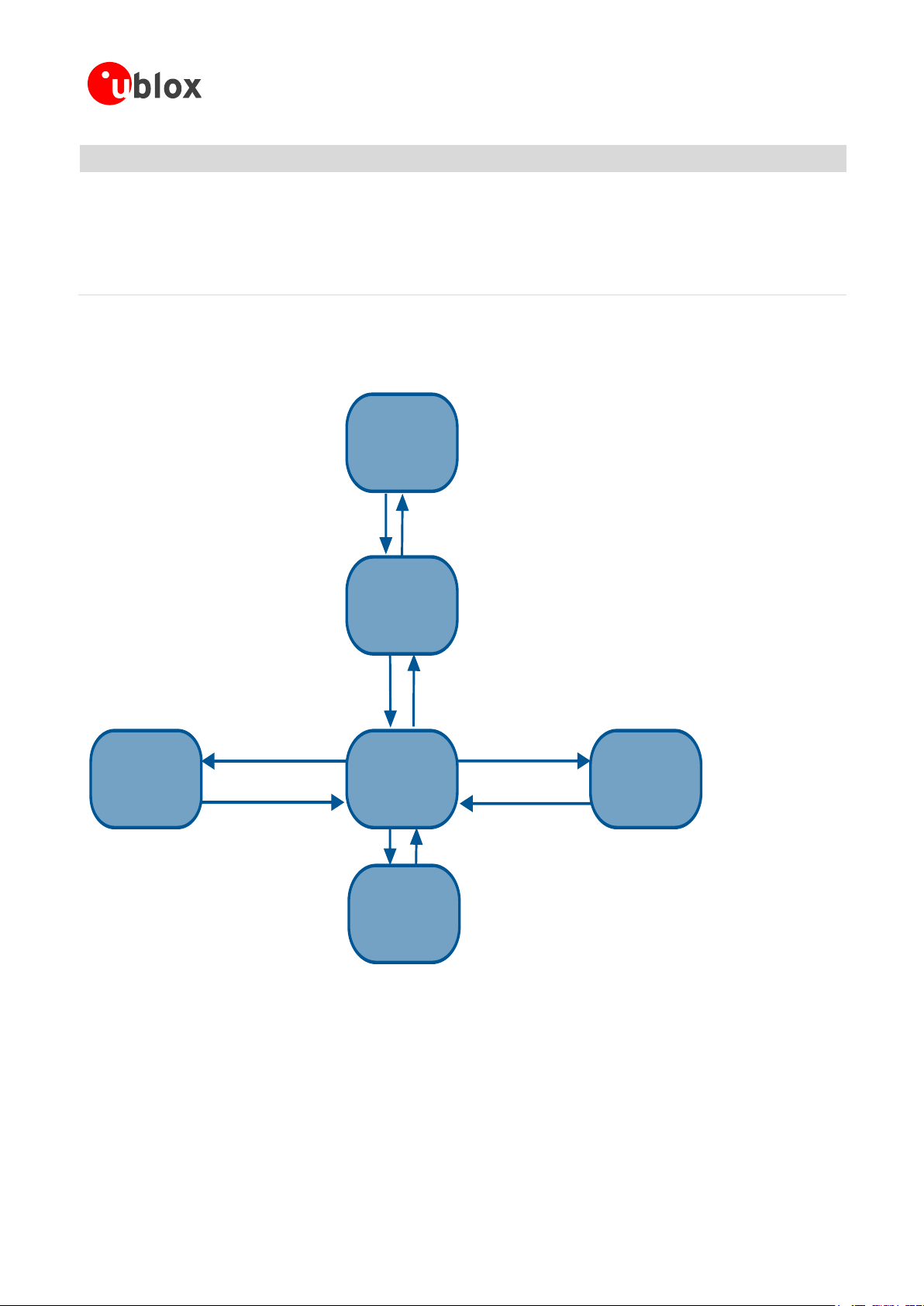
1.2 Architecture
Wireless
Base-band
Processor
Memory
Power Management Unit
26 MHz
32.768 kHz
ANT1
RF
Transceiver
ANT2
V_INT (I/O)
V_BCKP
VCC (Supply)
(U)SIM Card
USB
GPIO *
Power On
External Reset
PA
LNA Filter
Filter
Duplexer
Filter
PA
LNA Filter
Filter
Duplexer
Filter
LNA FilterFilter
LNA FilterFilter
Switch
Switch
Wireless
Base-band
Processor
Memory
Power Management Unit
26 MHz
32.768 kHz
ANT1
RF
Transceiver
ANT2
V_INT (I/O)
V_BCKP
VCC
(Supply)
(U)SIM Card
USB
GPIO *
Power On
External Reset
PA
LNA Filter
Filter
Duplexer
Filter
PA
LNA Filter
Filter
Duplexer
Filter
LNA FilterFilter
LNA FilterFilter
LNA FilterFilter
PA
LNA Filter
Filter
Duplexer
Filter
Switch
Switch
TOBY-L1 series - System Integration Manual
Figure 1: TOBY-L100 block diagram
Figure 2: TOBY-L110 block diagram
* = GPIOs are not supported by initial FW release.
UBX-13001482 Objective Information System description
Page 9 of 85
Page 10

TOBY-L1 series - System Integration Manual
1.2.1 Internal blocks
TOBY-L1 series modules consist of the following internal sections: RF, Baseband and Power Management.
RF section
The RF section is composed of RF transceiver, filters, LNAs, PAs, duplexers and antenna switches.
FDD (frequency division duplex)RF transceiver performs modulation, up-conversion of the baseband I/Q
signals for TX, down-conversion and demodulation of the dual RF signals received. The RF transceiver
contains:
automatically gain controlled direct conversion Zero-IF receiver,
highly linear RF demodulator / modulator capable QPSK/16QAM/64QAM,
Fractional-N Sigma-Delta RF synthesizer,
VCO.
Tx signal is pre-amplified by RF transceiver, then connected to the primary antenna input/output port (ANT1) of
the module via power amplifier (PA), band specific duplexer and antenna switch.
Dual receiving paths are connected respectively to the primary (ANT1) and secondary (ANT2) antenna ports
via duplexer SAW (band pass) filters
26 MHz crystal oscillator generates the clock reference in active-mode or connected-mode.
Baseband section
The Baseband section is composed of the following main elements:
Baseband processors in a mixed signal ASIC, which integrates
microprocessor for control functions,
DSP core for LTE Layer 1 and digital processing of Rx and Tx signal paths,
memory interface controller,
dedicated peripheral blocks for control of the USB, USIM and GPIO digital interfaces,
analog front end interfaces to RF transceiver ASIC.
Memory system, which includes NAND flash and LPDDR.
Power Management section
The Power Management section is composed of the following elements:
Voltage regulators to derive all the system supply voltages from the module supply input VCC
Voltage sources for external use: V_BCKP and V_INT
Hardware power on
Hardware reset
Low power idle-mode support
TOBY-L1 series modules are provided with an internal 32.768 kHz crystal oscillator to provide the clock reference
in the low power idle-mode, which can be set with power saving configuration enabled by the AT+UPSV
command.
UBX-13001482 Objective Information System description
Page 10 of 85
Page 11

TOBY-L1 series - System Integration Manual
Function
Pin Name
Module
Pin No
I/O
Description
Remarks
Power
VCC
All
70,71,72
I
Module supply
input
VCC pins are internally connected each other.
VCC supply circuit affects the RF performance and
compliance of the device integrating the module
with applicable required certification schemes.
See section 1.5.1 for functional description and
requirements for the VCC module supply.
See section 2.1.1 for external circuit design-in.
GND
All
2, 30, 32,
44, 46, 69,
73, 74, 76,
78, 79, 80,
82, 83, 85,
86, 88-90,
92-152
N/A
Ground
GND pins are internally connected each other.
External ground connection affects the RF and
thermal performance of the device.
See section 1.5.1 for functional description.
See section 2.1.1 for external circuit design-in.
V_BCKP
All 3 O
RTC supply
output
V_BCKP = 2.5 V (typical) generated by internal
regulator when valid VCC supply is present.
See section 1.5.2 for functional description.
See section 2.1.2 for external circuit design-in.
V_INT
All 5 O
Digital Interfaces
supply output
V_INT = 1.8 V (typical) generated by internal
regulator when the module is switched on.
See section 1.5.3 for functional description.
See section 2.1.3 for external circuit design-in.
System
PWR_ON
All
20 I Power-on input
High impedance input: input voltage level has to be
properly fixed, e.g. adding an external pull-up
resistor to the V_BCKP output pin
See section 1.6.1 for functional description.
See section 2.2.1 for external circuit design-in.
RESET_N
All
23 I External reset
input
It is internally pulled up to V_BCKP with a 10 k
resistor.
See section 1.6.3 for functional description.
See section 2.2.2 for external circuit design-in.
RF
ANT1
All
81
I/O
Primary antenna
Main Tx / Rx antenna interface.
50 nominal characteristic impedance.
Antenna circuit affects the RF performance and
compliance of the device integrating the module
with applicable required certification schemes.
See section 1.7 for functional description and
requirements for the antenna RF interface.
See section 2.3 for external circuit design-in.
ANT2
All
87 I Secondary
antenna
Rx only for the MIMO 2x2 configuration.
50 nominal characteristic impedance.
Antenna circuit affects the RF performance and
compliance of the device integrating the module
with applicable required certification schemes.
See section 1.7 for functional description and
requirements for the antenna RF interface.
See section 2.3 for external circuit design-in.
1.3 Pin-out
Table 3 lists the pin-out of the TOBY-L1 series modules, with pins grouped by function.
UBX-13001482 Objective Information System description
Page 11 of 85
Page 12

TOBY-L1 series - System Integration Manual
Function
Pin Name
Module
Pin No
I/O
Description
Remarks
SIM
VSIM
All
59 O SIM supply
output
VSIM = 1.8 V / 3 V automatically generated
according to the connected SIM type.
See section 1.8 for functional description.
See section 2.4 for external circuit design-in.
SIM_IO
All
57
I/O
SIM data
Data input/output for 1.8 V / 3 V SIM
Internal 4.7 k pull-up to VSIM.
See section 1.8 for functional description.
See section 2.4 for external circuit design-in.
SIM_CLK
All
56 O SIM clock
5 MHz clock output for 1.8 V / 3 V SIM
See section 1.8 for functional description.
See section 2.4 for external circuit design-in.
SIM_RST
All
58 O SIM reset
Reset output for 1.8 V / 3 V SIM
See section 1.8 for functional description.
See section 2.4 for external circuit design-in.
USB
USB_D-
All
27
I/O
USB Data Line D-
90 Ω nominal differential impedance (Z0)
30 Ω nominal common mode impedance (ZCM)
Pull-up or pull-down resistors and external series
resistors as required by the USB 2.0 high-speed
specification [4] are part of the USB pad driver and
need not be provided externally.
See section 1.9.1 for functional description.
See section 2.5.1 for external circuit design-in.
USB_D+
All
28
I/O
USB Data Line D+
90 Ω nominal differential impedance (Z0)
30 Ω nominal common mode impedance (ZCM)
Pull-up or pull-down resistors and external series
resistors as required by the USB 2.0 high-speed
specification [4] are part of the USB pad driver and
need not be provided externally.
See section 1.9.1 for functional description.
See section 2.5.1 for external circuit design-in.
GPIO
GPIO1
All
21
I/O
GPIO
1.8 V GPIO by default configured as pad disabled.
See section 1.10 for functional description.
See section 2.6 for external circuit design-in.
GPIO2
All
22
I/O
GPIO
1.8 V GPIO by default configured as pad disabled.
See section 1.10 for functional description.
See section 2.6 for external circuit design-in.
GPIO3
All
24
I/O
GPIO
1.8 V GPIO by default configured as pad disabled.
See section 1.10 for functional description.
See section 2.6 for external circuit design-in.
GPIO4
All
25
I/O
GPIO
1.8 V GPIO by default configured as pad disabled.
See section 1.10 for functional description.
See section 2.6 for external circuit design-in.
GPIO5
All
60
I/O
GPIO
1.8 V GPIO by default configured as pad disabled.
See section 1.10 for functional description.
See section 2.6 for external circuit design-in.
GPIO6
All
61
I/O
GPIO
1.8 V GPIO by default configured as pad disabled.
See section 1.10 for functional description.
See section 2.6 for external circuit design-in.
Reserved
RSVD
All
1, 4, 6-19,
26, 29, 31,
33-43, 45,
47-55, 6268, 75, 77,
84, 91
N/A
RESERVED pin
Leave unconnected.
See section 2.7
Table 3: TOBY-L1 series modules pin definition, grouped by function
UBX-13001482 Objective Information System description
Page 12 of 85
Page 13

TOBY-L1 series - System Integration Manual
General Status
Operating Mode
Definition
Power-down
Not-Powered Mode
VCC supply not present or below operating range: module is switched off.
Power-Off Mode
VCC supply within operating range and module is switched off.
Normal Operation
Low Power-Mode
Module processor core runs with 32 kHz reference, that is generated by:
The internal 32 kHz oscillator
Idle-Mode
Module processor core runs with 26 MHz reference generated by the internal oscillator.
Connected-Mode
Data Connection enabled and processor core runs with 26 MHz reference.
Operating Mode
Description
Transition between operating modes
Not-Powered Mode
Module is switched off.
USB interface is not accessible.
When VCC supply is removed, the module enters
not-powered mode.
When in not-powered mode, the module cannot be
switched on by a low level on PWR_ON input.
When in not-powered mode, the module can be
switched on after applying VCC supply (refer to 2.2.1) so
that the module switches from not-powered to idlemode.
Power-Off Mode
Module is switched off: normal shutdown by an
appropriate power-off event (refer to 1.6.2).
USB interface is not accessible.
When the module is switched off by an appropriate
power-off event (refer to 1.6.2), the module enters
power-off mode from idle-mode.
When in power-off mode, the module can be switched
on by a low level on PWR_ON input from power-off to
idle-mode.
When VCC supply is removed, the module switches from
power-off mode to not-powered mode.
Idle-Mode
The module is ready to communicate with an external
device by means of the USB interface unless power
saving configuration is enabled by the AT+UPSV
command
Power saving configuration is not enabled by default: it
can be enabled by the AT+UPSV command (see TOBY-
L1xx AT Commands Manual [2]).
When the module is switched on by an appropriate
power-on event (refer to 2.2.1), the module enters idlemode from not-powered or power-off mode.
If power saving is enabled the module can transition
from Idle-Mode to Power save-mode (refer to the TOBY-
L1xx AT Commands Manual [2], AT+UPSV).
When a data Connection is initiated, the module
switches from idle-mode to connected-mode.
Power Save-Mode
The module is ready to communicate with an external
device by means of the USB interface
Power saving configuration is not enabled by default: it
can be enabled by the AT+UPSV command (see TOBY-
L1xx AT Commands Manual [2]).
When the module is commanded to enter power savemode from idle-mode by AT+UPSV=1
When the module is commanded to disable power savemode by AT+UPSV=0
Connected-Mode
A data connection is in progress.
The module is ready to communicate with an external
device by means of the USB interface unless power
saving configuration is enabled by the AT+UPSV
command (TOBY-L1xx AT Commands Manual [2]).
When a data connection is initiated, the module enters
connected-mode from idle-mode.
When a data connection is terminated, the module
returns to the idle-mode.
1.4 Operating modes
TOBY-L1 modules have several operating modes. The operating modes are defined in Table 4 and described in
details in Table 5, providing general guidelines for operation.
Table 4: Module operating modes definition
UBX-13001482 Objective Information System description
Page 13 of 85
Page 14
TOBY-L1 series - System Integration Manual
Operating Mode
Description
Transition between operating modes
Airplane-Mode
The module is ready to communicate with an external
device by means of the USB interface.
The module cannot register or connect to network.
Purpose is to inhibit RF reception and transmission.
When the module is commanded to enter airplane-mode
from idle-mode by AT+CFUN=0
When the module is commanded to leave airplane-mode
by AT+CFUN=1
Apply VCC
If power saving is enabled
and there is no activity for
a defined time interval
Any wake up event described
in the module operating
modes summary table above
Incoming/outgoing
connection
Connection terminated,
communication dropped
Remove VCC
Switch ON: PWR_ON
Not
powered
Power off
IdleConnected
Power
Save
Switch OFF: AT+CPWROFF
Airplane
Table 5: Module operating modes description
Figure 3 describes the transition between the different operating modes.
Figure 3: Operating modes transition
UBX-13001482 Objective Information System description
Page 14 of 85
Page 15

TOBY-L1 series - System Integration Manual
Item
Requirement
Remark
VCC nominal voltage
Within VCC normal operating range:
3.4 V min. / 4.50 V max.
The module cannot be switched on if VCC voltage value
is below the normal operating range minimum limit.
Ensure that the input voltage at VCC pins is above the
minimum limit of the normal operating range for at least
1 second before the module switch-on.
VCC average current
Considerably withstand maximum average current
consumption value in connected-mode conditions
specified in TOBY-L1 series Data Sheet [1].
The maximum average current consumption can be
greater than the specified value according to the actual
antenna mismatching, temperature and VCC voltage.
Chapter 1.5.1.2 describes connected-mode current.
1.5 Supply interfaces
1.5.1 Module supply input (VCC)
TOBY-L1 modules must be supplied via the three VCC pins that represent the module power supply input.
The VCC pins are internally connected to the integrated Power Management Unit. All supply voltages needed by
the module are generated from the VCC supply by integrated voltage regulators, including V_BCKP supply,
V_INT digital interface supply and VSIM SIM card supply.
During operation, the current drawn by the TOBY-L1 series modules through the VCC pins can vary by several
orders of magnitude. This range from the high peak of current consumption during LTE transmission bursts at
maximum power level in connected-mode (as described in the chapter 1.5.1.2), to the low current consumption
during low power save-mode with power saving enabled (as described in the chapter 1.5.1.3).
1.5.1.1 VCC supply requirements
Table 6 summarizes the requirements for the VCC module supply. Refer to chapter 2.1.1 for all the suggestions
to properly design a VCC supply circuit compliant to the requirements listed in Table 6.
The VCC supply circuit affects the RF compliance of the device integrating TOBY-L1 series
module with applicable required certification schemes as well as antenna circuit design.
Compliance is guaranteed if the VCC requirements summarized in the Table 6 are fulfilled.
Table 6: Summary of VCC supply requirements
1.5.1.2 VCC current consumption in connected-mode
When a LTE connection is established, the VCC consumption is determined by the current consumption profile
typical of the LTE transmitting and receiving bursts.
The current consumption peak during a transmission slot is strictly dependent on the transmitted power, which
is reflected by the network conditions.
Figure 4 shows an example of the module current consumption profile versus time in LTE connected-mode.
UBX-13001482 Objective Information System description
Page 15 of 85
Page 16

TOBY-L1 series - System Integration Manual
Time [ms]
RX
slot
unused
slot
unused
slot
TX
slot
unused
slot
unused
slot
MON
slot
unused
slot
RX
slot
unused
slot
unused
slot
TX
slot
unused
slot
unused
slot
MON
slot
unused
slot
GSM frame
4.615 ms
(1 frame = 8 slots)
Current [A]
200 mA
60-120 mA
1900 mA
Peak current
depends on
TX power
GSM frame
4.615 ms
(1 frame = 8 slots)
1.5
1.0
0.5
0.0
2.0
60-120 mA
10-40 mA
Figure 4: VCC current consumption profile versus time during a LTE Connection (1 TX slot, 1 RX slot)
UBX-13001482 Objective Information System description
Page 16 of 85
Page 17

TOBY-L1 series - System Integration Manual
~30 ms
IDLE MODE ACTIVE MODE IDLE MODE
400-700 µA
Active Mode
Enabled
Idle Mode
Enabled
400-700 µA
60-120 mA
0.44-2.09 s
IDLE MODE
~30 ms
ACTIVE MODE
Time [s]
Current [mA]
100
50
0
Time [ms]
Current [mA]
100
50
0
3-6 mA
7-18 mA
60-120 mA
PLL
Enabled
RX
Enabled
20-40 mA
DSP
Enabled
1.5.1.3 VCC current consumption in power save-mode (power saving enabled)
The power saving configuration is by default disabled, but it can be enabled using the appropriate AT command
(refer to TOBY-L1xx AT Commands Manual [2], AT+UPSV command). When power saving is enabled, the
module automatically enters power save-mode whenever possible, reducing current consumption.
During power save-mode, the module processor runs with 32 kHz reference clock frequency.
When power saving is enabled, the module is registered or attached to a network and a data Connection is not
enabled, the module automatically enters power save-mode whenever possible, but it must periodically monitor
the paging channel of the current base station (paging block reception), in accordance to LTE system
requirements. When the module monitors the paging channel, it wakes up to idle-mode, to enable the reception
of paging block. In between, the module switches to power save-mode..
Figure 5: Description of VCC current consumption profile versus time when the module is registered the network: the module is
in idle-mode and periodically wakes up to active-mode to monitor the paging channel for paging block reception
UBX-13001482 Objective Information System description
Page 17 of 85
Page 18

TOBY-L1 series - System Integration Manual
ACTIVE MODE
7-18 mA
60-120 mA
0.47-2.12 s
Paging period
Time [s]
Current [mA]
100
50
0
Time [ms]
Current [mA]
100
50
0
7-18 mA
60-120 mA
RX
Enabled
20-40 mA
DSP
Enabled
7-18 mA
1.5.1.4 VCC current consumption in fixed active-mode (power saving disabled)
Power saving configuration is by default disabled, or it can be disabled using the appropriate AT command (refer
to TOBY-L1xx AT Commands Manual [2], AT+UPSV command). When power saving is disabled, the module does
not automatically enter power save-mode whenever possible: the module remains in idle-mode.
The module processor core is activated during idle-mode, and the 26 MHz reference clock frequency is used.
Figure 6 shows an example of the module current consumption profile when power saving is disabled: the
module is registered with the network, idle-mode is maintained, and the receiver and the DSP are periodically
activated to monitor the paging channel for paging block reception.
Figure 6: Description of the VCC current consumption profile versus time when power saving is disabled: the active-mode is
always held, and the receiver and the DSP are periodically activated to monitor the paging channel for paging block reception
UBX-13001482 Objective Information System description
Page 18 of 85
Page 19

TOBY-L1 series - System Integration Manual
Baseband
Processor
70
VCC
71
VCC
72
VCC
3
V_BCKP
Linear
LDO
RTC
Power
Management
TOBY-L1
32 kHz
Baseband
Processor
70
VCC
71
VCC
72
VCC
5
V_INT
Switching
StepDown
Digital I/O
Interfaces
Power
Management
TOBY-L1 series
1.5.2 2.5V Supply Output (V_BCKP)
The V_BCKP pin of TOBY-L1 modules connected to internal 2.5v supply for customer use. This supply is
internally generated by a linear LDO regulator integrated in the Power Management Unit, as shown in Figure 7.
The output of this linear regulator is always enabled when the main voltage supply provided to the module
through the VCC pins is within the valid operating range.
Figure 7: TOBY-L1 series (V_BCKP) simplified block diagram
1.5.3 1.8V Supply Output (V_INT)
The 1.8 V voltage supply used internally to source the digital interfaces of TOBY-L1 modules is also available on
the V_INT supply output pin, as described in Figure 8.
Figure 8: TOBY-L1 series interfaces supply output (V_INT) simplified block diagram
The internal regulator that generates the V_INT supply is a switching step-down converter that is directly
supplied from VCC. The voltage regulator output is set to 1.8 V (typical) when the module is switched on and it
is disabled when the module is switched off.
The switching regulator operates in Pulse Width Modulation (PWM) for greater efficiency at high output loads
when the module is in connected-mode. When the module is in low power save-mode between paging periods
and with power saving configuration enabled by the appropriate AT command, it automatically switches to a
power save mode for greater efficiency at low output loads. Refer to the TOBY-L1xx AT Commands Manual [2],
+UPSV command.
UBX-13001482 Objective Information System description
Page 19 of 85
Page 20

TOBY-L1 series - System Integration Manual
VCC
V_BCKP
PWR_ON
V_INT
Internal Reset
System State
BB Pads State
Internal reset → Operational Operational
OFF
ON
Tristate with a PD
Internal reset
Start-up
event
Start of interface
configuration
All interfaces
are configured
4.5 ms
1.6 System function interfaces
1.6.1 Module power-on
The power-on sequence of TOBY-L1 series modules is initiated by
Low level on the PWR_ON pin (normally high with external pull-up) for an appropriate time period.
1.6.1.1 Low level on PWR_ON
When a TOBY-L1 module is in the power-off mode (i.e. switched off with valid VCC supply maintained), the
module can be switched on by forcing a low level on the PWR_ON input pin for at least 5 seconds.
The input voltage thresholds are tolerant of voltages up to the module supply level. The detailed electrical
characteristics are described in TOBY-L1 series Data Sheet [1].
There is no internal pull-up resistor on the PWR_ON pin: the pin has high input impedance and is weakly pulled
to the high level by the internal circuit. Therefore the external circuit must be able to hold the high logic level
stable, e.g. providing an external pull-up resistor (for further design-in guidelines refer to chapter 2.2.1).
1.6.1.2 Additional considerations
The module can be switched on from power-off mode by forcing a proper start-up event (e.g. PWR_ON low).
After the detection of a start-up event, all the module digital pins are held in tri-state until all the internal LDO
voltage regulators are turned on in a defined power-on sequence. Anyway it is highly suggested to not force any
logical state at pins input to avoid latch-up situations before the module is operational.
Then, as described in Figure 9, the baseband core is still held in reset state for a time interval: the internal reset
signal (which is not available on a module pin) is still low and all the digital pins of the module are held in reset
state. The reset state of all the digital pins is reported in the pin description table of TOBY-L1 Series Data
Sheet [1]. When the internal signal is released, the configuration of the module interfaces starts: during this
phase any digital pin is set in a proper sequence from the reset state to the default operational configuration.
After the internal reset is at high level, interface configuration sequence starts at that time we have to ensure
low level on the PWR_ON for 5 seconds (worst case). Finally, the module is fully ready to operate when all
interfaces are configured.
Figure 9: TOBY-L1 series power-on sequence description
UBX-13001482 Objective Information System description
Page 20 of 85
Page 21

TOBY-L1 series - System Integration Manual
VCC
V_BCKP
RESET_N
PWR_ON
V_INT
Internal Reset
System State
BB Pads State Operational
OFF
Tristate with a PD
ON
Operational → Tristate with a PD
RESET_N set low
value
~110 ms
Power off
The Internal Reset signal is available as soon as low level on PWR_ON pin is applyed, you can also monitor
the V_INT pin to sense start of the TOBY-L1 series power-on sequence.
1.6.2 Module power-off
An under-voltage shutdown occurs on TOBY-L1 modules when the VCC supply is removed, but in this case the
current parameter settings are not saved in the module’s non-volatile memory and a proper network detach
cannot be performed.
Figure 10 describes the power-off sequence by means of low level on RESET_N pin (normally high by internal
pull-up). At the end of the switch-off routine, all digital pins are locked in tri-state by the module and all the
internal LDO voltage regulators except V_BCKP are turned off in a defined power-off sequence. The module
remains in power off mode as long as a switch on event does not occur (i.e. applying a low level on the
PWR_ON pin), and enters not-powered mode if the supply is removed from the VCC pin.
Figure 10: TOBY-L1 series power-off sequence description
1.6.3 Module reset
A TOBY-L1 module reset can be performed in one of two ways.
RESET_N input pin: Forces a low level on the RESET_N input pin, causing an “external” or “hardware” reset.
This must be low for at least xx ms. This causes an asynchronous reset of the module baseband processor,
excluding the integrated Power Management Unit. The V_INT interfaces supply is enabled and each digital pin is
set in its reset state, the V_BCKP supply is enabled. Forcing an “external” or “hardware” reset, the current
parameter settings are not saved in the module’s non-volatile memory and a proper network detach is not
performed.
AT+CFUN command (refer to the TOBY-L1xx AT Commands Manual [2] for more details): This command
causes an “internal” or “software” reset, which is an asynchronous reset of the module baseband processor.
The electrical behavior is the same as that of the “external” or “hardware” reset, but in an “internal” or
“software” reset the current parameter settings are saved in the module’s non-volatile memory and a proper
network detach is performed.
UBX-13001482 Objective Information System description
Page 21 of 85
Page 22

TOBY-L1 series - System Integration Manual
Baseband
Processor
18
RESET_N
Reset Input
TOBY-L1 series
10k
2.5 V
After either reset, when RESET_N is released from the low level, the module automatically starts its power-on
sequence from the reset state.
The reset state of all digital pins is reported in the pin description table in TOBY-L1 series Data Sheet [1].
As described in Figure 11, the module has an internal pull-up resistor which pulls the line to the high logic level
when the RESET_N pin is not forced low from the external. Detailed electrical characteristics are described in
TOBY-L1 series Data Sheet [1].
Figure 11: TOBY-L1 series reset input (RESET_N) description
UBX-13001482 Objective Information System description
Page 22 of 85
Page 23

TOBY-L1 series - System Integration Manual
Item
Requirements
Remarks
Impedance
50 nominal characteristic impedance
The impedance of the antenna RF connection must match
the 50 impedance of the ANT pin.
Frequency Range
Module dependent
The required frequency range of the antenna depends on
the operating bands of the used TOBY-L1 module and the
used Mobile Network.
V.S.W.R
Return Loss
< 2:1 recommended, < 3:1 acceptable
S11 < -10 dB recommended, S11 < -6 dB acceptable
The impedance of the antenna termination must match as
much as possible the 50 impedance of the ANT pin over
the operating frequency range.
Input Power
> 1 W peak
The antenna termination must withstand the maximum
peak of power transmitted by TOBY-L1 modules.
Gain
Below the levels reported in the chapter 4.2.2
The antenna gain must not exceed the herein specified
value to comply with regulatory agencies radiation
exposure limits.
1.7 Antenna interface
1.7.1 Antenna RF interfaces (ANT1 / ANT2)
The ANT pins of TOBY-L1 modules represents the RF input/output for transmission and reception of the LTE RF
signals. The ANT pin has a nominal characteristic impedance of 50 and must be connected to the antenna
through a 50 transmission line to allow proper RF transmission and reception in operating bands.
1.7.1.1 Antenna RF interface requirements
Table 7 summarizes the requirements for the antenna RF interface (ANT). Refer to section 2.3.1 for suggestions
to properly design an antenna circuit compliant to these requirements.
The antenna circuit affects the RF compliance of the device integrating TOBY-L1 series module
with applicable required certification schemes. Compliance is guaranteed if the antenna RF
interface (ANT1 / ANT2 ) requirements summarized in Table 7 are fulfilled.
Table 7: Summary of antenna RF interface (ANT) requirements
1.8 SIM interface
1.8.1 SIM card interface
TOBY-L1 modules provide high-speed SIM/ME interface including automatic detection and configuration of the
voltage required by the connected SIM card or chip.
Both 1.8 V and 3 V SIM types are supported: activation and deactivation with automatic voltage switch from
1.8 V to 3 V is implemented, according to ISO-IEC 7816-3 specifications. The VSIM supply output pin provides
internal short circuit protection to limit start-up current and protect the device in short circuit situations.
The SIM driver supports the PPS (Protocol and Parameter Selection) procedure for baud-rate selection, according
to the values determined by the SIM Card.
SIM Application Toolkit (R99) is supported.
1.8.2 SIM card detection
UBX-13001482 Objective Information System description
Page 23 of 85
Page 24

TOBY-L1 series - System Integration Manual
The SIM card detection function determined via firmware after power on of module.
UBX-13001482 Objective Information System description
Page 24 of 85
Page 25

TOBY-L1 series - System Integration Manual
Name
Description
Remarks
USB_D+
USB Data Line D+
90 Ω nominal differential characteristic impedance (Z0)
30 Ω nominal common mode characteristic impedance (ZCM)
Pull-up or pull-down resistors and external series resistors as
required by the USB 2.0 high-speed specification [4] are part
of the USB pad driver and need not be provided externally.
USB_D-
USB Data Line D-
90 Ω nominal differential characteristic impedance (Z0)
30 Ω nominal common mode characteristic impedance (ZCM)
Pull-up or pull-down resistors and external series resistors as
required by the USB 2.0 high-speed specification [4] are part
of the USB pad driver and need not be provided externally.
1.9 Serial interfaces
TOBY-L1 series modules provide the following serial communication interface:
USB interface: 4-wire
1.9.1 USB
TOBY-L1 modules provide a high-speed USB interface at 480 Mb/s compliant with the Universal Serial Bus
Revision 2.0 specification [4]. It acts as a USB device and can be connected to any USB host such as a PC or other
Application Processor.
The USB-device shall look for all upper-SW-layers like any other serial device. This means that TOBY-L series
modules emulate all serial control logical lines.
Table 8: USB pins
The USB interface pins ESD sensitivity rating is 1 kV (Human Body Model according to JESD22-A114F).
Higher protection level could be required if the lines are externally accessible on the application board.
Higher protection level can be achieved by mounting a very low capacitance (i.e. less or equal to 1 pF)
ESD protection (e.g. Tyco Electronics PESD0402-140 ESD protection device) on the lines connected to
these pins, close to accessible points.
1.9.1.1 USB features
TOBY-L1 modules simultaneously supports 3 USB CDC (Communications Device Class) that assure multiple
functionalities to the USB physical interface. The 3 available CDCs are configured as described in the following
list:
USB1: Remote NDIS based Internet Sharing Device ( Ethernet connection )
USB2: Gadget Serial ( AT Commands )
USB3: Multifunction Gadget with multiple configurations
The module firmware can be upgraded over the USB interface using the u-blox EasyFlash tool Firmware Update
Application Note [11]).
UBX-13001482 Objective Information System description
Page 25 of 85
Page 26

TOBY-L1 series - System Integration Manual
USB CDC/ACM drivers are available for the following operating system platforms:
Windows XP
Windows 7
Standard Linux/Android USB kernel drivers
TOBY-L1 module identifies itself by its VID (Vendor ID) and PID (Product ID) combination, included in the USB
device descriptor.
VID and PID of TOBY-L1 modules are the following:
VID = 0x1546
PID = 0x1131 for TOBY-L100 series
PID = 0x1131 for TOBY-L110 series
1.9.1.2 USB and power saving
If power saving is enabled by AT command (AT+UPSV=1), the TOBY-L1 module automatically enters the USB
suspended state when the device has observed no bus traffic for a specified period (refer to the Universal Serial
Bus Revision 2.0 specification [4]). In suspended state, the module maintains any internal status as USB device,
including its address and configuration. In addition, the module enters the suspended state when the hub port it
is attached to is disabled: this is referred to as USB selective suspend. The module exits suspend mode when
there is bus activity.
TOBY-L1 module is capable of USB remote wake-up signaling: i.e. may request the host to exit suspend mode or
selective suspend by using electrical signaling to indicate remote wake-up. This notifies the host that it should
resume from its suspended mode, if necessary, and service the external event that triggered the suspended USB
device to signal the host. Remote wake-up is accomplished using electrical signaling described in the Universal
Serial Bus Revision 2.0 specification [4].
When the USB enters suspended state, the average VCC module current consumption of TOBY-L1 module is
~400 µA higher then when the USB is not attached to a USB host.
If power saving is disabled by AT+UPSV=0 and the TOBY-L1 module is attached to a USB host as USB device, is
configured and is not suspended, the average VCC module current consumption in fixed active mode is
increased to ~40 mA.
UBX-13001482 Objective Information System description
Page 26 of 85
Page 27

TOBY-L1 series - System Integration Manual
1.10 General Purpose Input/Output (GPIO)
TOBY-L1 modules may support functionality in future software release.
1.11 Reserved pins (RSVD)
TOBY-L1 modules have pins reserved for future use: they can all be left unconnected on the application board.
UBX-13001482 Objective Information System description
Page 27 of 85
Page 28

1.12 System features
1.12.1 Network indication
Not supported by TOBY-L1 modules.
TOBY-L1 series - System Integration Manual
UBX-13001482 Objective Information System description
Page 28 of 85
Page 29

TOBY-L1 series - System Integration Manual
1.12.2 TCP/IP and UDP/IP
Via the AT commands it is possible to access the TCP/IP and UDP/IP functionalities over the Packet Switched data
connection. For more details about AT commands see the TOBY-L1xx AT Commands Manual [2].
Using the embedded TCP/IP or UDP/IP stack, only 1 IP instance (address) is supported. The IP instance supports
up to 7 sockets. Using an external TCP/IP stack (on the application processor), it is possible to have 3 IP instances
(addresses).
Direct Link mode for TCP and UDP sockets is supported. Sockets can be set in Direct Link mode to establish a
transparent end-to-end communication with an already connected TCP or UDP socket via serial interface. In
Direct Link mode, data sent to the serial interface from an external application processor is forwarded to the
network and vice-versa.
To avoid data loss while using Direct Link, enable HW flow control on the serial interface.
1.12.3 FTP
TOBY-L1 modules support the File Transfer Protocol functionalities via AT commands. Files are read and stored in
the local file system of the module. For more details about AT commands see the TOBY-L1xx AT Commands
Manual [2].
1.12.4 HTTP
HTTP client is implemented in TOBY-L1 modules: HEAD, GET, POST, DELETE and PUT operations are available.
The file size to be uploaded / downloaded depends on the free space available in the local file system (FFS) at the
moment of the operation. Up to 4 HTTP client contexts can simultaneously be used.
For more details about AT commands see the TOBY-L1xx AT Commands Manual [2].
1.12.5 SMTP
Not supported by TOBY-L1 modules.
1.12.6 Firmware upgrade Over The Air (FOTA)
This feature allows upgrading the module Firmware over the air, i.e. over the LTE network. The main idea with
updating Firmware over the air is to reduce the amount of data required for transmission to the module. This is
achieved by downloading only a “delta file” instead of the full firmware. The delta contains only the differences
between the two firmware versions (old and new), and is compressed.
For more details, refer to the Firmware Update Application Note [11].
1.12.7 Power saving
The power saving configuration is by default disabled, but it can be enabled using the AT+UPSV command.
When power saving is enabled, the module automatically enters the low power save-mode whenever possible,
reducing current consumption.
UBX-13001482 Objective Information System description
Page 29 of 85
Page 30

TOBY-L1 series - System Integration Manual
During low power save-mode, the module is not ready to communicate with an external device by means of the
USB interface, since it is configured to reduce power consumption. It can be woken up from power save-mode
to idle-mode by the connected application processor or by network activities, as described in the Table 5.
During power save-mode, the module processor core runs on the 32 kHz reference clock.
For the complete description of the AT+UPSV command, refer to the TOBY-L1xx AT Commands Manual [2].
For the definition and the description of TOBY-L1 series modules operating modes, including the events forcing
transitions between the different operating modes, refer to the chapter 1.4.
For the description of current consumption in idle and active operating modes, refer to chapters 1.5.1.2, 1.5.1.4.
UBX-13001482 Objective Information System description
Page 30 of 85
Page 31

TOBY-L1 series - System Integration Manual
2 Design-in
For an optimal integration of TOBY-L1 modules in the final application board follow the design guidelines stated
in this chapter.
Every application circuit must be properly designed to guarantee the correct functionality of the relative
interface, however a number of points require high attention during the design of the application device.
The following list provides a ranking of importance in the application design, starting from the highest relevance:
1. Module antenna connection: ANT1 and ANT2 pins. Antenna circuit directly affects the RF compliance of the
device integrating TOBY-L1 module with applicable certification schemes. Very carefully follow the
suggestions provided in the relative chapter 2.3 for schematic and layout design.
2. Module supply: VCC and GND pins. The supply circuit affects the RF compliance of the device integrating
TOBY-L1 module with applicable required certification schemes as well as antenna circuit design. Very
carefully follow the suggestions provided in the relative chapter 2.1.1 for schematic and layout design.
3. SIM card interface: VSIM, SIM_CLK, SIM_IO, SIM_RST pins. Accurate design is required to guarantee SIM
card functionality reducing the risk of RF coupling. Carefully follow the suggestions provided in the relative
chapter 2.4 for schematic and layout design.
4. System functions: RESET_N, PWR_ON pins. Accurate design is required to guarantee that the voltage level
is well defined during operation. Carefully follow the suggestions provided in the relative chapter 2.2 for
schematic and layout design.
5. Other supplies: the V_BCKP supply output and the V_INT digital interfaces supply output. Accurate design
is required to guarantee proper functionality. Follow the suggestions provided in the relative chapters 2.1.2
and 2.1.3 for schematic and layout design.
UBX-13001482 Objective Information Design-in
Page 31 of 85
Page 32

TOBY-L1 series - System Integration Manual
Main Supply
Available?
Battery
Li-Ion 3.7 V
Linear LDO
Regulator
Main Supply
Voltage
>5 V?
Switching
Step-Down
Regulator
No, portable device
No, less than 5 V
Yes, greater than 5 V
Yes, always available
2.1 Supply interfaces
2.1.1 Module supply (VCC)
2.1.1.1 General guidelines for VCC supply circuit selection and design
VCC pins are internally connected, but connect all the available pads to the external supply to minimize the
power loss due to series resistance.
GND pins are internally connected but connect all the available pads to solid ground on the application board,
since a good (low impedance) connection to external ground can minimize power loss and improve RF and
thermal performance.
TOBY-L1 modules must be supplied through the VCC pins by a proper DC power supply that should meet the
following prerequisites to comply with the module VCC requirements summarized in Table 6.
The proper DC power supply can be selected according to the application requirements (see Figure 12) between
the different possible supply sources types, which most common ones are the following:
Switching regulator
Low Drop-Out (LDO) linear regulator
Rechargeable Lithium-ion (Li-Ion) or Lithium-ion polymer (Li-Pol) battery
Primary (disposable) battery
Figure 12: VCC supply concept selection
The switching step-down regulator is the typical choice when the available primary supply source has a nominal
voltage much higher (e.g. greater than 5 V) than the TOBY-L1 modules operating supply voltage. The use of
switching step-down provides the best power efficiency for the overall application and minimizes current drawn
from the main supply source.
The use of an LDO linear regulator becomes convenient for a primary supply with a relatively low voltage (e.g.
less than 5 V). In this case the typical 90% efficiency of the switching regulator diminishes the benefit of voltage
step-down and no true advantage is gained in input current savings. On the opposite side, linear regulators are
not recommended for high voltage step-down as they dissipate a considerable amount of energy in thermal
power.
If TOBY-L1 modules are deployed in a mobile unit where no permanent primary supply source is available, then a
battery will be required to provide VCC. A standard 3-cell Li-Ion or Li-Pol battery pack directly connected to VCC
is the usual choice for battery-powered devices. During charging, batteries with Ni-MH chemistry typically reach
a maximum voltage that is above the maximum rating for VCC, and should therefore be avoided.
UBX-13001482 Objective Information Design-in
Page 32 of 85
Page 33

TOBY-L1 series - System Integration Manual
The use of primary (not rechargeable) battery is uncommon, since the most cells available are seldom capable of
delivering the burst peak current for a LTE Connection due to high internal resistance.
Keep in mind that the use of batteries requires the implementation of a suitable charger circuit (not included in
TOBY-L1 modules). The charger circuit should be designed in order to prevent over-voltage on VCC beyond the
upper limit of the absolute maximum rating.
The usage of more than one DC supply at the same time should be carefully evaluated: depending on the supply
source characteristics, different DC supply systems can result as mutually exclusive.
The usage of a regulator or a battery not able to withstand the maximum peak current consumption specified in
the TOBY-L1 series Data Sheet [1] is generally not recommended. However, if the selected regulator or battery is
not able to withstand the maximum peak current of the module, it must be able to considerably withstand at
least the maximum average current consumption value specified in the TOBY-L1 series Data Sheet [1], and the
additional energy required by the module during a LTE Tx slot (when the current consumption can rise up to
1.9 A in the worst case, as described in section 1.5.1.2) could be provided by a proper bypass tank capacitor
with very large capacitance and very low ESR (depending on the actual capability of the selected regulator or
battery, the required capacitance can be considerably larger than 1 mF) placed close to the module VCC pins.
Carefully evaluate the implementation of this solution since the aging and temperature conditions highly affects
the actual capacitors characteristics.
The following sections highlight some design aspects for each of the supplies listed above providing application
circuit design-in compliant with the module VCC requirements summarized in Table 6.
2.1.1.2 Guidelines for VCC supply circuit design using a switching regulator
The use of a switching regulator is suggested when the difference from the available supply rail to the VCC value
is high: switching regulators provide good efficiency transforming a 12 V or greater voltage supply to the typical
3.8 V value of the VCC supply.
The characteristics of the switching regulator connected to VCC pins should meet the following prerequisites to
comply with the module VCC requirements summarized in Table 6:
Power capability: the switching regulator with its output circuit must be capable of providing a voltage
value to the VCC pins within the specified operating range and must be capable of delivering 1.9 A current
pulses with 1/8 duty cycle to the VCC pins
Low output ripple: the switching regulator together with its output circuit must be capable of providing a
clean (low noise) VCC voltage profile
High switching frequency: for best performance and for smaller applications select a switching frequency
≥ 600 kHz (since L-C output filter is typically smaller for high switching frequency). The use of a switching
regulator with a variable switching frequency or with a switching frequency lower than 600 kHz must be
carefully evaluated since this can produce noise in the VCC voltage profile and therefore negatively impact
LTE modulation spectrum performance. An additional L-C low-pass filter between the switching regulator
output to VCC supply pins can mitigate the ripple on VCC, but adds extra voltage drop due to resistive
losses on series inductors
PWM mode operation: it is preferable to select regulators with Pulse Width Modulation (PWM) mode.
While in connected-mode Pulse Frequency Modulation (PFM) mode and PFM/PWM mode, transitions must
be avoided to reduce the noise on the VCC voltage profile. Switching regulators that are able to switch
between low ripple PWM mode and high efficiency burst or PFM mode can be used, provided the mode
transition occurs when the module changes status from idle/active-mode to connected-mode (where current
consumption increases to a value greater than 100 mA): it is permissible to use a regulator that switches
from the PWM mode to the burst or PFM mode at an appropriate current threshold (e.g. 60 mA)
Output voltage slope: the use of the soft start function provided by some voltage regulators should be
carefully evaluated, since the VCC pins voltage must ramp from 2.5 V to 3.2 V within 4 ms to switch on the
module that otherwise can be switched on by a low level on PWR_ON pin
UBX-13001482 Objective Information Design-in
Page 33 of 85
Page 34

TOBY-L1 series - System Integration Manual
Please leave width at 16.9cm (17cm = .docx page width) to preserve 1:1 scaling
12V
C
5
R
3
C
4
R
2
C
2
C
1
R
1
VIN
RUN
VC
RT
PG
SYNC
BD
BOOS
T
SW
FB
GN
D
6
7
10
9
5
C
6
1
2
3
8
11
4
C
7
C
8
D
1
R
4
R
5
L1
C
3
U
1
TOBY-L1 series
71
VCC
72
VCC
70
VCC
GND
Reference
Description
Part Number - Manufacturer
C1
10 µF Capacitor Ceramic X7R 5750 15% 50 V
C5750X7R1H106MB - TDK
C2
10 nF Capacitor Ceramic X7R 0402 10% 16 V
GRM155R71C103KA01 - Murata
C3
680 pF Capacitor Ceramic X7R 0402 10% 16 V
GRM155R71H681KA01 - Murata
C4
22 pF Capacitor Ceramic C0G 0402 5% 25 V
GRM1555C1H220JZ01 - Murata
C5
10 nF Capacitor Ceramic X7R 0402 10% 16 V
GRM155R71C103KA01 - Murata
C6
470 nF Capacitor Ceramic X7R 0603 10% 25 V
GRM188R71E474KA12 - Murata
C7
22 µF Capacitor Ceramic X5R 1210 10% 25 V
GRM32ER61E226KE15 - Murata
C8
330 µF Capacitor Tantalum D_SIZE 6.3 V 45 mΩ
T520D337M006ATE045 - KEMET
D1
Schottky Diode 40 V 3 A
MBRA340T3G - ON Semiconductor
L1
10 µH Inductor 744066100 30% 3.6 A
744066100 - Wurth Electronics
R1
470 kΩ Resistor 0402 5% 0.1 W
2322-705-87474-L - Yageo
R2
15 kΩ Resistor 0402 5% 0.1 W
2322-705-87153-L - Yageo
R3
22 kΩ Resistor 0402 5% 0.1 W
2322-705-87223-L - Yageo
R4
390 kΩ Resistor 0402 1% 0.063 W
RC0402FR-07390KL - Yageo
R5
100 kΩ Resistor 0402 5% 0.1 W
2322-705-70104-L - Yageo
U1
Step-Down Regulator MSOP10 3.5 A 2.4 MHz
LT3972IMSE#PBF - Linear Technology
Figure 13 and the components listed in Table 9 show an example of a high reliability power supply circuit, where
the module VCC is supplied by a step-down switching regulator capable of delivering 1.9 A current pulses with
low output ripple and with fixed switching frequency in PWM mode operation greater than 1 MHz.
Figure 13: Suggested schematic design for the VCC voltage supply application circuit using a step-down regulator
Table 9: Suggested components for the VCC voltage supply application circuit using a step-down regulator
UBX-13001482 Objective Information Design-in
Page 34 of 85
Page 35

TOBY-L1 series - System Integration Manual
Please leave width at 16.9cm (17cm = .docx page width) to preserve 1:1 scaling
12V
R
5
C
6
C
1
VCC
INH
FSW
SYNC
OUT
GN
D
2
6
3
1
7
8
C
3
C
2
D
1
R
1
R
2
L1
U
1
FB
COMP
5
4
R
3
C
4
R
4
C
5
TOBY-L1 series
71
VCC
72
VCC
70
VCC
GND
Reference
Description
Part Number - Manufacturer
C1
22 µF Capacitor Ceramic X5R 1210 10% 25 V
GRM32ER61E226KE15 – Murata
C2
100 µF Capacitor Tantalum B_SIZE 20% 6.3V 15m
T520B107M006ATE015 – Kemet
C3
5.6 nF Capacitor Ceramic X7R 0402 10% 50 V
GRM155R71H562KA88 – Murata
C4
6.8 nF Capacitor Ceramic X7R 0402 10% 50 V
GRM155R71H682KA88 – Murata
C5
56 pF Capacitor Ceramic C0G 0402 5% 50 V
GRM1555C1H560JA01 – Murata
C6
220 nF Capacitor Ceramic X7R 0603 10% 25 V
GRM188R71E224KA88 – Murata
D1
Schottky Diode 25V 2 A
STPS2L25 – STMicroelectronics
L1
5.2 µH Inductor 30% 5.28A 22 m
MSS1038-522NL – Coilcraft
R1
4.7 k Resistor 0402 1% 0.063 W
RC0402FR-074K7L – Yageo
R2
910 Resistor 0402 1% 0.063 W
RC0402FR-07910RL – Yageo
R3
82 Resistor 0402 5% 0.063 W
RC0402JR-0782RL – Yageo
R4
8.2 k Resistor 0402 5% 0.063 W
RC0402JR-078K2L – Yageo
R5
39 k Resistor 0402 5% 0.063 W
RC0402JR-0739KL – Yageo
U1
Step-Down Regulator 8-VFQFPN 3 A 1 MHz
L5987TR – ST Microelectronics
Figure 14 and the components listed in Table 10 show an example of a low cost power supply circuit, where the
VCC module supply is provided by a step-down switching regulator capable of delivering 1.9 A current pulses,
transforming a 12 V supply input.
Figure 14: Suggested low cost solution for the VCC voltage supply application circuit using step-down regulator
Table 10: Suggested components for low cost solution VCC voltage supply application circuit using a step-down regulator
2.1.1.3 Guidelines for VCC supply circuit design using a Low Drop-Out (LDO) linear regulator
The use of a linear regulator is suggested when the difference from the available supply rail and the VCC value is
low: linear regulators provide high efficiency when transforming a 5 V supply to a voltage value within the
module VCC normal operating range.
The characteristics of the LDO linear regulator connected to the VCC pins should meet the following
prerequisites to comply with the module VCC requirements summarized in Table 6:
Power capabilities: the LDO linear regulator with its output circuit must be capable of providing a proper
voltage value to the VCC pins and of delivering 1.9 A current pulses with 1/8 duty cycle
Power dissipation: the power handling capability of the LDO linear regulator must be checked to limit its
junction temperature to the maximum rated operating range (i.e. check the voltage drop from the max input
voltage to the min output voltage to evaluate the power dissipation of the regulator)
UBX-13001482 Objective Information Design-in
Page 35 of 85
Page 36

TOBY-L1 series - System Integration Manual
Please leave width at 16.9cm (17cm = .docx page width) to preserve 1:1 scaling
5V
C
1
R1
IN OUT
ADJ
GN
D
1
2
4
5
3
C
2
R2
R3
U
1
SHD
N
TOBY-L1 series
71
VCC
72
VCC
70
VCC
GND
C
3
Reference
Description
Part Number - Manufacturer
C1, C2
10 µF Capacitor Ceramic X5R 0603 20% 6.3 V
GRM188R60J106ME47 - Murata
C3
330 µF Capacitor Tantalum D_SIZE 6.3 V 45 mΩ
T520D337M006ATE045 - KEMET
R1
47 kΩ Resistor 0402 5% 0.1 W
RC0402JR-0747KL - Yageo Phycomp
R2
9.1 kΩ Resistor 0402 5% 0.1 W
RC0402JR-079K1L - Yageo Phycomp
R3
3.9 kΩ Resistor 0402 5% 0.1 W
RC0402JR-073K9L - Yageo Phycomp
U1
LDO Linear Regulator ADJ 3.0 A
LT1764AEQ#PBF - Linear Technology
Output voltage slope: the use of the soft start function provided by some voltage regulator should be
carefully evaluated, since the VCC pins voltage must ramp from 2.5 V to 3.2 V within 4 ms to switch-on the
module that otherwise can be switched on by a low level on PWR_ON pin
Figure 15 and the components listed in Table 11 show an example of a power supply circuit, where the VCC
module supply is provided by an LDO linear regulator capable of delivering 1.9 A current pulses, with proper
power handling capability.
It is recommended to configure the LDO linear regulator to generate a voltage supply value slightly below the
maximum limit of the module VCC normal operating range (e.g. ~4.1 V as in the circuit described in Figure 15
and Table 11). This reduces the power on the linear regulator and improves the thermal design of the supply
circuit.
Figure 15: Suggested schematic design for the VCC voltage supply application circuit using an LDO linear regulator
Table 11: Suggested components for VCC voltage supply application circuit using an LDO linear regulator
2.1.1.4 Guidelines for VCC supply circuit design using a rechargeable Li-Ion or Li-Pol battery
Rechargeable Li-Ion or Li-Pol batteries connected to the VCC pins should meet the following prerequisites to
comply with the module VCC requirements summarized in Table 6:
Maximum pulse and DC discharge current: the rechargeable Li-Ion battery with its output circuit must be
capable of delivering 1.9 A current pulses with 1/8 duty-cycle to the VCC pins and must be capable of
delivering a DC current greater than the module maximum average current consumption to VCC pins. The
maximum pulse discharge current and the maximum DC discharge current are not always reported in
battery data sheets, but the maximum DC discharge current is typically almost equal to the battery capacity
in Amp-hours divided by 1 hour
DC series resistance: the rechargeable Li-Ion battery with its output circuit must be capable of avoiding a
VCC voltage drop greater than 400 mV during transmit bursts
2.1.1.5 Guidelines for VCC supply circuit design using a primary (disposable) battery
The characteristics of a primary (non-rechargeable) battery connected to VCC pins should meet the following
prerequisites to comply with the module VCC requirements summarized in Table 6:
UBX-13001482 Objective Information Design-in
Page 36 of 85
Page 37

TOBY-L1 series - System Integration Manual
Maximum pulse and DC discharge current: the non-rechargeable battery with its output circuit must be
capable of delivering 1.9 A current pulses with 1/8 duty-cycle to the VCC pins and must be capable of
delivering a DC current greater than the module maximum average current consumption at the VCC pins.
The maximum pulse and the maximum DC discharge current is not always reported in battery data sheets,
but the maximum DC discharge current is typically almost equal to the battery capacity in Amp-hours
divided by 1 hour
DC series resistance: the non-rechargeable battery with its output circuit must be capable of avoiding a
VCC voltage drop greater than 400 mV during transmit bursts
2.1.1.6 Additional guidelines for VCC supply circuit design
To reduce voltage drops, use a low impedance power source. The resistance of the power supply lines
(connected to the VCC and GND pins of the module) on the application board and battery pack should also be
considered and minimized: cabling and routing must be as short as possible to minimize power losses.
Three pins are allocated for VCC supply. Another twenty pins are designated for GND connection. Even if all the
VCC pins and all the GND pins are internally connected within the module, it is recommended to properly
connect all of them to supply the module to minimize series resistance losses.
To avoid voltage drop undershoot and overshoot at the start and end of a transmit burst during a LTE
Connection (when current consumption on the VCC supply can rise up to as much as 1.9 A in the worst case),
place a bypass capacitor with large capacitance (more than 100 µF) and low ESR near the VCC pins, for example:
330 µF capacitance, 45 m ESR (e.g. KEMET T520D337M006ATE045, Tantalum Capacitor)
The use of very large capacitors (i.e. greater then 1000 µF) on the VCC line should be carefully evaluated, since
the voltage at the VCC pins must ramp from 2.5 V to 3.2 V within 4 ms to switch on the module that otherwise
can be switched on by a low level on PWR_ON pin.
To reduce voltage ripple and noise, especially if the application device integrates an internal antenna, place the
following bypass capacitors near the VCC pins:
100 nF capacitor (e.g Murata GRM155R61C104K) to filter digital logic noise from clocks and data sources
10 nF capacitor (e.g. Murata GRM155R71C103K) to filter digital logic noise from clocks and data sources
56 pF capacitor with Self-Resonant Frequency in 800/900 MHz range (e.g. Murata GRM1555C1E560J) to
filter transmission EMI in the LTE/ELTE bands
15 pF capacitor with Self-Resonant Frequency in 1800/1900 MHz range (e.g. Murata GRM1555C1E150J) to
filter transmission EMI in the DCS/PCS bands
Figure 16 shows the complete configuration but the mounting of each single component depends on the
application design: it is recommended to provide all the VCC bypass capacitors as described in Figure 16
and Table 12 if the application device integrates an internal antenna.
UBX-13001482 Objective Information Design-in
Page 37 of 85
Page 38

TOBY-L1 series - System Integration Manual
C
4
GND
C3C
2
TOBY-L1 series
71
VCC
72
VCC
70
VCC
3V8
C
1
+
C
5
Reference
Description
Part Number - Manufacturer
C1
330 µF Capacitor Tantalum D_SIZE 6.3 V 45 mΩ
T520D337M006ATE045 - KEMET
C2
100 nF Capacitor Ceramic X7R 0402 10% 16 V
GRM155R71C104KA01 - Murata
C3
10 nF Capacitor Ceramic X7R 0402 10% 16 V
GRM155R71C103KA01 - Murata
C4
56 pF Capacitor Ceramic C0G 0402 5% 25 V
GRM1555C1E560JA01 - Murata
C5
15 pF Capacitor Ceramic C0G 0402 5% 25 V
GRM1555C1E150JA01 - Murata
Figure 16: Suggested schematic and layout design for the VCC bypass capacitors to reduce ripple / noise on VCC voltage profile
and to avoid undershoot / overshoot on VCC voltage drops
Table 12: Suggested components to reduce ripple / noise on VCC and to avoid undershoot/ overshoot on VCC voltage drops
ESD sensitivity rating of the VCC supply pins is 1 kV (Human Body Model according to JESD22-A114).
2.1.1.7 Guidelines for external battery charging circuit
TOBY-L1 modules do not have an on-board charging circuit. Figure 17 provides an example of a battery charger
design, suitable for applications that are battery powered with a Li-Ion (or Li-Polymer) cell.
In the application circuit, a rechargeable Li-Ion (or Li-Polymer) battery cell, that features proper pulse and DC
discharge current capabilities and proper DC series resistance, is directly connected to the VCC supply input of
TOBY-L1 module. Battery charging is completely managed by the STMicroelectronics L6924U Battery Charger IC
that, from a USB power source (5.0 V typ.), charges as a linear charger the battery, in three phases:
Pre-charge constant current (active when the battery is deeply discharged): the battery is charged with a
Fast-charge constant current: the battery is charged with the maximum current, configured by the value
Constant voltage: when the battery voltage reaches the regulated output voltage (4.2 V), the L6924U
Using a battery pack with an internal NTC resistor, the L6924U can monitor the battery temperature to protect
the battery from operating under unsafe thermal conditions.
Alternatively the L6924U, providing input voltage range up to 12 V, can charge from an AC wall adapter. When
a current-limited adapter is used, it can operate in quasi-pulse mode, reducing power dissipation.
UBX-13001482 Objective Information Design-in
Page 38 of 85
Higher protection level can be required if the line is externally accessible on the application board, e.g. if
accessible battery connector is directly connected to VCC pins. Higher protection level can be achieved by
mounting an ESD protection (e.g. EPCOS CA05P4S14THSG varistor array) close to accessible point.
low current, set to 10% of the fast-charge current
of an external resistor to a value suitable for USB power source (~500 mA)
starts to reduce the current until the charge termination is done. The charging process ends when the
charging current reaches the value configured by an external resistor to ~15 mA or when the charging timer
reaches the value configured by an external capacitor to ~9800 s
Page 39

C
5
C
8
GND
C7C
6
C
9
TOBY-L1 series
71
VCC
72
VCC
70
VCC
+
USB
Supply
C
3
R
4
θ
U
IUSB
IAC
IEND
TPRG
SD
VIN
VINSNS
MODE
ISEL
C
2
C
1
5V
0
TH
GND
VOUT
VOSNS
VREF
R
1
R
2
R
3
Li-Ion/Li-Pol
Battery
Pack
D
1
B1
C
4
Li-Ion/Li-Polymer
Battery Charger
IC
Figure 17: Li-Ion (or Li-Polymer) battery charging application circuit
Reference
Description
Part Number - Manufacturer
B1
Li-Ion (or Li-Polymer) battery pack with 470 NTC
Various manufacturer
C1, C4
1 µF Capacitor Ceramic X7R 0603 10% 16 V
GRM188R71C105KA12 - Murata
C2, C6
10 nF Capacitor Ceramic X7R 0402 10% 16 V
GRM155R71C103KA01 - Murata
C3
1 nF Capacitor Ceramic X7R 0402 10% 50 V
GRM155R71H102KA01 - Murata
C5
330 µF Capacitor Tantalum D_SIZE 6.3 V 45 m
T520D337M006ATE045 - KEMET
C7
100 nF Capacitor Ceramic X7R 0402 10% 16 V
GRM155R61A104KA01 - Murata
C8
56 pF Capacitor Ceramic C0G 0402 5% 25 V
GRM1555C1E560JA01 - Murata
C9
15 pF Capacitor Ceramic C0G 0402 5% 25 V
GRM1555C1E150JA01 - Murata
D1
Low Capacitance ESD Protection
USB0002RP or USB0002DP - AVX
R1, R2
24 k Resistor 0402 5% 0.1 W
RC0402JR-0724KL - Yageo Phycomp
R3
3.3 k Resistor 0402 5% 0.1 W
RC0402JR-073K3L - Yageo Phycomp
R4
1.0 k Resistor 0402 5% 0.1 W
RC0402JR-071K0L - Yageo Phycomp
U1
Single Cell Li-Ion (or Li-Polymer) Battery Charger IC
for USB port and AC Adapter
L6924U - STMicroelectronics
TOBY-L1 series - System Integration Manual
Table 13: Suggested components for Li-Ion (or Li-Polymer) battery charging application circuit
2.1.1.8 Guidelines for VCC supply layout design
Good connection of the module VCC pins with DC supply source is required for correct RF performance.
Guidelines are summarized in the following list:
All the available VCC pins must be connected to the DC source
VCC connection must be as wide as possible and as short as possible
Any series component with Equivalent Series Resistance (ESR) greater than few milliohms must be avoided
VCC connection must be routed through a PCB area separated from sensitive analog signals and sensitive
functional units: it is good practice to interpose at least one layer of PCB ground between VCC track and
other signal routing
Coupling between VCC and audio lines (especially microphone inputs) must be avoided, because the typical
LTE burst has a periodic nature of approx. 217 Hz, which lies in the audible audio range
The tank bypass capacitor with low ESR for current spikes smoothing described in Figure 16 and Table 12
should be placed close to the VCC pins. If the main DC source is a switching DC-DC converter, place the
large capacitor close to the DC-DC output and minimize the VCC track length. Otherwise consider using
separate capacitors for DC-DC converter and TOBY-L1 module tank capacitor
The bypass capacitors in the pF range described in Figure 16 and Table 12 should be placed as close as
possible to the VCC pins. This is highly recommended if the application device integrates an internal antenna
UBX-13001482 Objective Information Design-in
Page 39 of 85
Page 40

TOBY-L1 series - System Integration Manual
Since VCC is directly connected to RF Power Amplifiers, voltage ripple at high frequency may result in
unwanted spurious modulation of transmitter RF signal. This is more likely to happen with switching DC -DC
converters, in which case it is better to select the highest operating frequency for the switcher and add a
large L-C filter before connecting to the TOBY-L1 series modules in the worst case
If VCC is protected by transient voltage suppressor to ensure that the voltage maximum ratings are not
exceeded, place the protecting device along the path from the DC source toward the TOBY-L1 module,
preferably closer to the DC source (otherwise protection functionality may be compromised)
2.1.1.9 Guidelines for grounding layout design
Good connection of the module GND pins with application board solid ground layer is required for correct RF
performance. It significantly reduces EMC issues and provides a thermal heat sink for the module.
Connect each GND pin with application board solid GND layer. It is strongly recommended that each GND
pad surrounding VCC pins have one or more dedicated via down to the application board solid ground layer
The VCC supply current flows back to main DC source through GND as ground current: provide adequate
return path with suitable uninterrupted ground plane to main DC source
If the application board is a multilayer PCB, then it is required to connect together each GND area with
complete via stack down to main board ground layer
It is recommended to implement one layer of the application board as ground plane as wide as possible
Good grounding of GND pads also ensures thermal heat sink. This is critical during Connection connection,
when the real network commands the module to transmit at maximum power: proper grounding helps
prevent module overheating
2.1.2 2.5V supply (V_BCKP)
2.1.2.1 Guidelines for V_BCKP circuit design
On TOBY-L100 and TOBY-L110 modules, the V_BCKP supply output can be used to for external customer use.
The internal regulator for V_BCKP is optimized for low leakage current and very light loads. Do not apply
loads which might exceed the limit for maximum available current from V_BCKP supply, as this can cause
malfunctions in the module. TOBY-L1 series Data Sheet [1] describes the detailed electrical characteristics.
V_BCKP supply output pin provides internal short circuit protection to limit start-up current and protect the
device in short circuit situations. No additional external short circuit protection is required.
ESD sensitivity rating of the V_BCKP supply pin is 1 kV (Human Body Model according to JESD22-A114).
Higher protection level can be required if the line is externally accessible on the application board, e.g. if
an accessible back-up battery connector is directly connected to V_BCKP pin. Higher protection level can
be achieved by mounting an ESD protection (e.g. EPCOS CA05P4S14THSG varistor array) close to the
accessible point.
2.1.2.2 Guidelines for V_BCKP layout design
V_BCKP supply requires careful layout: avoid injecting noise on this voltage domain as it may affect the stability
of the internal circuitry.
UBX-13001482 Objective Information Design-in
Page 40 of 85
Page 41

TOBY-L1 series - System Integration Manual
2.1.3 1.8V supply (V_INT)
2.1.3.1 Guidelines for V_INT circuit design
The V_INT digital interfaces 1.8 V supply output can be mainly used to:
Supply voltage translators to connect digital interfaces of the module to a 3.0 V device (see section 2.5.1)
Indicate when the module is switched on
Do not apply loads which might exceed the limit for maximum available current from V_INT supply, as
this can cause malfunctions in internal circuitry supplies to the same domain. TOBY-L1 series Data
Sheet [1] describes the detailed electrical characteristics.
V_INT can only be used as an output; do not connect any external regulator on V_INT.
Since the V_INT supply is generated by an internal switching step-down regulator, the V_INT voltage ripple can
range from 15 mVpp during active-mode or connected-mode (when the switching regulator operates in PWM
mode), to 90 mVpp in idle-mode (when the switching regulator operates in PFM mode).
It is not recommended to supply sensitive analog circuitry without adequate filtering for digital noise.
V_INT supply output pin provides internal short circuit protection to limit start-up current and protect the device
in short circuit situations. No additional external short circuit protection is required.
ESD sensitivity rating of the V_INT supply pin is 1 kV (Human Body Model according to JESD22-A114).
Higher protection level could be required if the line is externally accessible on the application board.
Higher protection level can be achieved by mounting an ESD protection (e.g. EPCOS CA05P4S14THSG
varistor array) close to accessible point.
If the V_INT supply output is not required by the customer application, since DDC (I
detection functions are not used and voltage translation of digital interfaces are not needed, the V_INT
pin can be left unconnected to external components, but it is recommended providing direct access on
the application board by means of accessible testpoint directly connected to the V_INT pin.
2.1.3.2 Guidelines for V_INT layout design
V_INT digital interfaces supply output is generated by an integrated switching step-down converter, used
internally to supply the digital interfaces. Because of this, it can be a source of noise: avoid coupling with
sensitive signals.
2
C) interface and SIM
UBX-13001482 Objective Information Design-in
Page 41 of 85
Page 42
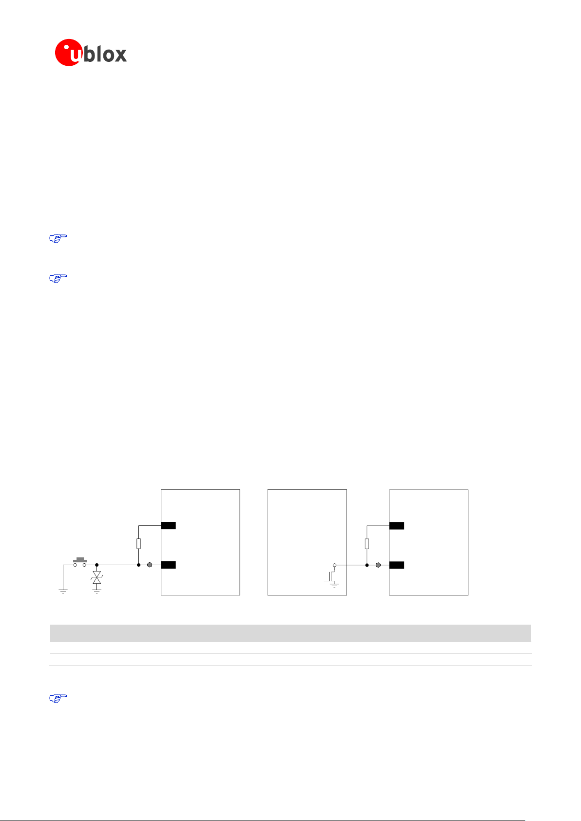
TOBY-L1 series - System Integration Manual
2.2.1.2
Please leave width at 16.9cm (17cm = .docx page width) to preserve 1:1 scaling
TOB-L1 series
Rex
t
3
V_BCKP
20
PWR_ON
Power-on
push button
ES
D
Open
Drain
Output
Application
Processor
TOBY-L1 series
Rex
t
3
V_BCKP
20
PWR_ON
TP
TP
Reference
Description
Remarks
Rext
100 kΩ Resistor 0402 5% 0.1 W
External pull-up resistor
ESD
CT0402S14AHSG - EPCOS
Varistor array for ESD protection
2.2 System functions interfaces
2.2.1 Module power-on (PWR_ON)
2.2.1.1 Guidelines for PWR_ON circuit design
and Table 14. Connecting the PWR_ON input to a push button, the pin will be externally accessible on the
application device: according to EMC/ESD requirements of the application, provide an additional ESD protection
(e.g. EPCOS CA05P4S14THSG varistor array) on the line connected to this pin, close to accessible point.
Pull-up resistor (e.g. 100 kΩ) biased by the V_BCKP supply pin of the module, as described in Figure 18
The PWR_ON pin has high input impedance and is weakly pulled to the high level on the module. Avoid
keeping it floating in a noisy environment. To hold the high logic level stable, the PWR_ON pin must be
connected to a pull-up resistor (e.g. 100 kΩ) biased by the V_BCKP supply pin of the module.
ESD sensitivity rating of the PWR_ON pin is 1 kV (Human Body Model according to JESD22-A114). Higher
protection level can be required if the line is externally accessible on the application board, e.g. if an
accessible push button is directly connected to PWR_ON pin. Higher protection level can be achieved by
mounting an ESD protection (e.g. EPCOS CA05P4S14THSG varistor array) close to accessible point.
Connecting the PWR_ON input to an external device (e.g. application processor), use an open drain output on
the external device with an external pull-up resistor (e.g. 100 kΩ) biased by the V_BCKP supply pin of the
module, as described in Figure 18 and Table 14.
A compatible push-pull output of an application processor can also be used: in this case the pull-up can be
provided to pull the PWR_ON level high when the application processor is switched off. If the high-level voltage
of the push-pull output pin of the application processor is greater than the maximum input voltage operating
range of the V_BCKP pin (refer to TOBY-L1 series Data Sheet [1]), the V_BCKP supply cannot be used to bias the
pull-up resistor: the supply rail of the application processor or the module VCC supply could be used, but this
increases the V_BCKP current consumption when the module is in not-powered mode (VCC supply not present).
Using a push-pull output of the external device, take care to fix the proper level in all the possible scenarios to
avoid an inappropriate module switch-on.
Figure 18: PWR_ON application circuits using a push button and an open drain output of an application processor
Table 14: Example of pull-up resistor and ESD protection for the PWR_ON application circuit
It is recommended to provide direct access to the PWR_ON pin on the application board by means of
accessible testpoint directly connected to the PWR_ON pin.
UBX-13001482 Objective Information Design-in
Page 42 of 85
Page 43
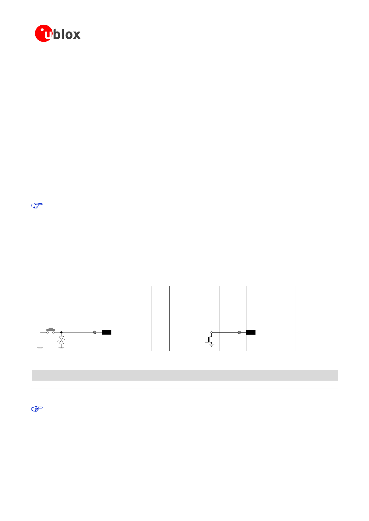
TOBY-L1 series - System Integration Manual
Please leave width at 16.9cm (17cm = .docx page width) to preserve 1:1 scaling
TOBY-L1 series
18
RESET_
N
Reset
push button
ES
D
Open
Drain
Output
Application
Processor
TOBY-L1 series
18
RESET_
N
TP
TP
Reference
Description
Remarks
ESD
Varistor for ESD protection
CT0402S14AHSG - EPCOS
2.2.1.3 Guidelines for PWR_ON layout design
The power-on circuit (PWR_ON) requires careful layout since it is the sensitive input available to switch on the
TOBY-L1 modules until a valid VCC supply is provided after that the module has been switched off by means of
the AT+CPWROFF command: ensure that the voltage level is well defined during operation and no transient
noise is coupled on this line, otherwise the module might detect a spurious power-on request.
2.2.2 Module reset (RESET_N)
2.2.2.1 Guidelines for RESET_N circuit design
As described in Figure 11, the module has an internal pull-up resistor on the reset input line: an external pull-up
is not required on the application board.
Connecting the RESET_N input to a push button that shorts the RESET_N pin to ground, the pin will be
externally accessible on the application device: according to EMC/ESD requirements of the application, provide
an additional ESD protection (e.g. EPCOS CA05P4S14THSG varistor array) on the line connected to this pin, close
to accessible point, as described in Figure 19 and Table 15.
ESD sensitivity rating of the RESET_N pin is 1 kV (Human Body Model according to JESD22-A114). Higher
protection level can be required if the line is externally accessible on the application board, e.g. if an
accessible push button is directly connected to RESET_N pin. Higher protection level can be achieved by
mounting an ESD protection (e.g. EPCOS CA05P4S14THSG varistor array) close to accessible point.
Connecting the RESET_N input to an external device (e.g. application processor), an open drain output can be
directly connected without any external pull-up, as described in Figure 19 and Table 15: the internal pull-up
resistor provided by the module pulls the line to the high logic level when the RESET_N pin is not forced low by
the application processor. A compatible push-pull output of an application processor can be used too.
Figure 19: RESET_N application circuits using a push button and an open drain output of an application processor
Table 15: Example of ESD protection component for the RESET_N application circuit
If the external reset function is not required by the customer application, the RESET_N input pin can be
left unconnected to external components, but it is recommended providing direct access on the
application board by means of accessible testpoint directly connected to the RESET_N pin.
UBX-13001482 Objective Information Design-in
Page 43 of 85
Page 44

TOBY-L1 series - System Integration Manual
2.2.2.2 Guidelines for RESET_N layout design
The reset circuit (RESET_N) requires careful layout due to the pin function: ensure that the voltage level is well
defined during operation and no transient noise is coupled on this line, otherwise the module might detect a
spurious reset request. It is recommended to keep the connection line to RESET_N as short as possible.
UBX-13001482 Objective Information Design-in
Page 44 of 85
Page 45

TOBY-L1 series - System Integration Manual
2.3 Antenna interface
The ANT1 ANT2 pins, provided by all TOBY-L1 modules, represent the main RF inputs/output used to transmit
and receive the LTE RF signals. The primary antenna must be connected. The ANT pin has a nominal
characteristic impedance of 50 and must be connected to the antenna through a 50 transmission line to
allow transmission and reception of radio frequency (RF) signals in operating bands.
2.3.1 Antenna RF interface (ANT)
2.3.1.1 General guidelines for antenna selection and design
The LTE antenna is the most critical component to be evaluated. Designers must take care of the antenna from
all perspective at the very start of the design phase when the physical dimensions of the application board are
under analysis/decision, since the RF compliance of the device integrating TOBY-L1 module with all the
applicable required certification schemes depends from antenna radiating performance.
LTE antennas are typically available in the typies of linear monopole and path antenna.
Linear monopole - External antenna
o External antenna basically does not imply physical restriction to the design of the PCB where the
TOBY-L1 series module is mounted.
o The radiation performance mainly depends on the antenna. It is required to select the antenna
with optimal radiating performance in the operating bands.
o An RF cable should be selected with minimum insertion loss due to the additional insertion loss
introduced by low quality or long cable. Large insertion loss reduces radiation performance.
o A high quality 50 RF connector provides proper PCB-to-RF-cable transition. It is recommended to
strictly follow the layout guidelines provided by the connector manufacturer.
Patch-like antenna - Integrated antenna:
o Internal integrated antenna implies physical restriction to the design of the PCB. The ground plane
can be reduced down to a minimum size that must be similar to the quarter of the wavelength of
the minimum frequency that has to be radiated. As numerical example:
Frequency = 1 GHz Wavelength = 30 cm Minimum GND plane size = 7.5 cm
o The radiation performance depends on the whole PCB and antenna system design, including
product mechanical design and usage. The antenna should be selected with optimal radiating
performance in the operating bands according to the mechanical specifications of the PCB and the
whole product.
o It is recommended to select a complete custom antenna designed by an antenna manufacturer if
the required ground plane dimensions are very small (e.g. less than 6.5 cm long and 4 cm wide).
The antenna design process should begin at the start of the whole product design process
o It is highly recommended to strictly follow the detailed and specific guidelines provided by the
antenna manufacturer regarding correct installation and deployment of the antenna system,
including PCB layout and matching circuitry
o Further to the custom PCB and product restrictions, the antenna may require a tuning to comply
with all the applicable required certification schemes. It is recommended to consult the antenna
manufacturer for the design-in guidelines for antenna matching relative to the custom application
In both cases, selecting an external or an internal antenna, these recommendations should be observed:
Select an antenna providing optimal return loss (or V.S.W.R.) figure over all the operating frequencies,
Select an antenna providing optimal efficiency figure over all the operating frequencies,
UBX-13001482 Objective Information Design-in
Page 45 of 85
Page 46
TOBY-L1 series - System Integration Manual
GND clearance on buried layer
below ANT pad
GND
Min.
250 µm
Min. 400 µm
GND clearance on top layer
around ANT pad
Select an antenna providing appropriate gain figure (i.e. combined antenna directivity and efficiency figure)
so that the electromagnetic field radiation intensity do not exceed the regulatory limits specified in some
countries (e.g. by FCC in the United States, as reported in the chapter 4.2.2).
2.3.1.2 Guidelines for antenna RF interface design
Guidelines for ANT pin RF connection design
Proper transition between the ANT pad and the application board PCB must be provided, implementing the
following design-in guidelines for the layout of the application PCB close to the ANT pad:
On a multi layer board, the whole layer stack below the RF connection should be free of digital lines
Increase GND keep-out (i.e. clearance, a void area) around the ANT pad, on the top layer of the application
PCB, to at least 250 µm up to adjacent pads metal definition and up to 400 µm on the area below the
module, to reduce parasitic capacitance to ground, as described in the left picture in Figure 20
Add GND keep-out (i.e. clearance, a void area) on the buried metal layer below the ANT pad if the top-layer
to buried layer dielectric thickness is below 200 µm, to reduce parasitic capacitance to ground, as described
in the right picture in Figure 20
Figure 20: GND keep-out area on the top layer around ANT pad and on the very close buried layer below ANT pad
Guidelines for RF transmission line design
The transmission line from the ANT pad up to antenna connector or up to the internal antenna pad must be
designed so that the characteristic impedance is as close as possible to 50 .
The transmission line can be designed as a micro strip (consists of a conducting strip separated from a ground
plane by a dielectric material) or a strip line (consists of a flat strip of metal which is sandwiched between two
parallel ground planes within a dielectric material). The micro strip, implemented as a coplanar waveguide, is the
most common configuration for printed circuit board.
UBX-13001482 Objective Information Design-in
Page 46 of 85
Page 47

TOBY-L1 series - System Integration Manual
35 um
35 um
35 um
35 um
270 um
270 um
760 um
L1 Copper
L3 Copper
L2 Copper
L4 Copper
FR-4 dielectric
FR-4 dielectric
FR-4 dielectric
380 um 500 um500 um
35 um
35 um
1510 um
L2 Copper
L1 Copper
FR-4 dielectric
1200 um 400 um400 um
Figure 21 and Figure 22 provide two examples of proper 50 coplanar waveguide designs: the first transmission
line can be implemented in case of 4-layer PCB stack-up herein described, the second transmission line can be
implemented in case of 2-layer PCB stack-up herein described.
Figure 21: Example of 50 coplanar waveguide transmission line design for the described 4-layer board layup
Figure 22: Example of 50 coplanar waveguide transmission line design for the described 2-layer board layup
If the two examples do not match the application PCB stack-up the 50 characteristic impedance calculation
can be made using the HFSS commercial finite element method solver for electromagnetic structures from Ansys
Corporation, or using freeware tools like AppCAD from Agilent or TXLine from Applied Wave Research, taking
care of the approximation formulas used by the tools for the impedance computation.
To achieve a 50 characteristic impedance, the width of the transmission line must be chosen depending on:
the thickness of the transmission line itself (e.g. 35 µm in the example of Figure 21 and Figure 22)
the thickness of the dielectric material between the top layer (where the transmission line is routed) and the
inner closer layer implementing the ground plane (e.g. 270 µm in Figure 21, 1510 µm in Figure 22)
the dielectric constant of the dielectric material (e.g. dielectric constant of the FR-4 dielectric material in
Figure 21 and Figure 22)
the gap from the transmission line to the adjacent ground plane on the same layer of the transmission line
(e.g. 500 µm in Figure 21, 400 µm in Figure 22)
If the distance between the transmission line and the adjacent GND area (on the same layer) does not exceed 5
times the track width of the micro strip, use the “Coplanar Waveguide” model for the 50 calculation.
UBX-13001482 Objective Information Design-in
Page 47 of 85
Page 48

TOBY-L1 series - System Integration Manual
Not actual TOBY module series
SMA
connector
Additionally to the 50 impedance, the following guidelines are recommended for the transmission line design:
Minimize the transmission line length: the insertion loss should be minimized as much as possible, in the
order of a few tenths of a dB,
Add GND keep-out (i.e. clearance, a void area) on buried metal layers below any pad of component present
on the RF transmission line, if top-layer to buried layer dielectric thickness is below 200 µm, to reduce
parasitic capacitance to ground,
The transmission line width and spacing to GND must be uniform and routed as smoothly as possible: avoid
abrupt changes of width and spacing to GND,
Add GND stitching vias around transmission line, as described in Figure 23,
Ensure solid metal connection of the adjacent metal layer on the PCB stack-up to main ground layer,
providing enough on the adjacent metal layer, as described in Figure 23,
Route RF transmission line far from any noise source (as switching supplies and digital lines) and from any
sensitive circuit (as analog audio lines),
Avoid stubs on the transmission line,
Avoid signal routing in parallel to transmission line or crossing the transmission line on buried metal layer,
Do not route microstrip line below discrete component or other mechanics placed on top layer
An example of proper RF circuit design is reported in the Figure 23. In this case, the ANT pin is directly
connected to an SMA connector by means of a proper 50 transmission line, designed with proper layout.
Figure 23: Suggested circuit and layout for antenna RF circuit on application board, if antenna detection is not required
Guidelines for RF termination design
The RF termination must provide a characteristic impedance of 50 as well as the RF transmission line up to the
RF termination itself, to match the characteristic impedance of the ANT pin of TOBY-L1 modules.
However, real antennas have no perfect 50 load on all the supported frequency bands. Therefore, to reduce
as much as possible performance degradation due to antenna mismatch, the RF termination must provide
optimal return loss (or V.S.W.R.) figure over all the operating frequency bands, as summarized in Table 7.
UBX-13001482 Objective Information Design-in
Page 48 of 85
Page 49

TOBY-L1 series - System Integration Manual
If an external antenna is used, the antenna connector represents the RF termination on the PCB:
Use a suitable 50 connector providing proper PCB-to-RF-cable transition
Strictly follow the connector manufacturer’s recommended layout, for example:
o SMA Pin-Through-Hole connectors require GND keep-out (i.e. clearance, a void area) on all the
layers around the central pin up to annular pads of the four GND posts, as shown in Figure 23
o UFL surface mounted connectors require no conductive traces (i.e. clearance, a void area) in the
area below the connector between the GND land pads.
Cut out the GND layer under RF connectors and close to buried vias, to remove stray capacitance and thus
keep the RF line 50 , e.g. the active pad of UFL connectors needs to have a GND keep-out (i.e. clearance, a
void area) at least on first inner layer to reduce parasitic capacitance to ground.
If an integrated antenna is used, the RF termination is represented by the integrated antenna itself. The
following guidelines should be followed.
Use an antenna designed by an antenna manufacturer, providing the best possible return loss (or V.S.W.R.).
Provide a ground plane large enough according to the relative integrated antenna requirements. The ground
plane of the application PCB can be reduced down to a minimum size that must be similar to one quarter of
wavelength of the minimum frequency that has to be radiated. As numerical example,
Frequency = 1 GHz Wavelength = 30 cm Minimum GND plane size = 7.5 cm
It is highly recommended to strictly follow the detailed and specific guidelines provided by the antenna
manufacturer regarding correct installation and deployment of the antenna system, including PCB layout
and matching circuitry.
Further to the custom PCB and product restrictions, the antenna may require a tuning to comply with all the
applicable required certification schemes. It is recommended to consult the antenna manufacturer for the
design-in guidelines for the antenna matching relative to the custom application
Additionally, these recommendations regarding the antenna system placement must be followed:
Do not include antenna within closed metal case.
Do not place the antenna in close vicinity to end user since the emitted radiation in human tissue is limited
by regulatory requirements.
Place the antenna far from sensitive analog systems or employ countermeasures to reduce electromagnetic
compatibility issues.
Take care of interaction between co-located RF systems since the LTE transmitted power may interact or
disturb the performance of companion systems.
UBX-13001482 Objective Information Design-in
Page 49 of 85
Page 50

TOBY-L1 series - System Integration Manual
2.4 SIM interface
2.4.1.1 Guidelines for SIM circuit design
Guidelines for SIM cards, SIM connectors and SIM chips selection
The ISO/IEC 7816, the ETSI TS 102 221 and the ETSI TS 102 671 specifications define the physical, electrical and
functional characteristics of Universal Integrated Circuit Cards (UICC) which contains the Subscriber Identification
Module (SIM) integrated circuit that securely stores all the information needed to identify and authenticate
subscribers over the LTE network.
Removable UICC / SIM card contacts mapping is defined by ISO/IEC 7816 and ETSI TS 102 221as follows:
Contact C1 = VCC (Supply) It must be connected to VSIM
Contact C2 = RST (Reset) It must be connected to SIM_RST
Contact C3 = CLK (Clock) It must be connected to SIM_CLK
Contact C4 = AUX1 (Auxiliary contact) It must be left not connected
Contact C5 = GND (Ground) It must be connected to GND
Contact C6 = VPP (Programming supply) It must be left not connected
Contact C7 = I/O (Data input/output) It must be connected to SIM_IO
Contact C8 = AUX2 (Auxiliary contact) It must be left not connected
A removable SIM card can have 6 contacts (C1 = VCC, C2 = RST, C3 = CLK, C5 = GND, C6 = VPP, C7 = I/O) or
8 contacts, providing also the auxiliary contacts C4 = AUX1 and C8 = AUX2 for USB interfaces and other uses.
Only 6 contacts are required and must be connected to the module SIM card interface as described above, since
TOBY-L1 modules do not support the additional auxiliary features (contacts C4 = AUX1 and C8 = AUX2).
Removable SIM card are suitable for applications where the SIM changing is required during the product lifetime.
A SIM card holder can have 6 or 8 positions if a mechanical card presence detector is not provided, or it can
have 6+2 or 8+2 positions if two additional pins relative to the normally-open mechanical switch integrated in
the SIM connector for the mechanical card presence detection are provided: select a SIM connector providing
6+2 or 8+2 positions if the optional SIM detection feature is required by the custom application, otherwise a
connector without integrated mechanical presence switch can be selected.
Solderable UICC / SIM chip contacts mapping (M2M UICC Form Factor) is defined by ETSI TS 102 671 as follows:
Package Pin 8 = UICC Contact C1 = VCC (Supply) It must be connected to VSIM.
Package Pin 7 = UICC Contact C2 = RST (Reset) It must be connected to SIM_RST.
Package Pin 6 = UICC Contact C3 = CLK (Clock) It must be connected to SIM_CLK.
Package Pin 5 = UICC Contact C4 = AUX1 (Auxiliary contact) It must be left not connected.
Package Pin 1 = UICC Contact C5 = GND (Ground) It must be connected to GND.
Package Pin 2 = UICC Contact C6 = VPP (Programming supply) It must be connected to VSIM.
Package Pin 3 = UICC Contact C7 = I/O (Data input/output) It must be connected to SIM_IO.
Package Pin 4 = UICC Contact C8 = AUX2 (Auxiliary contact) It must be left not connected.
A solderable SIM chip has 8 contacts and can provide also the auxiliary contacts C4 = AUX1 and C8 = AUX2 for
USB interfaces and other uses, but only 6 contacts are required and must be connected to the module SIM card
interface as described above, since TOBY-L1 modules do not support the additional auxiliary features (contacts
C4 = AUX1 and C8 = AUX2).
Solderable SIM chips are suitable for M2M applications where it is not required to change the SIM once installed.
UBX-13001482 Objective Information Design-in
Page 50 of 85
Page 51
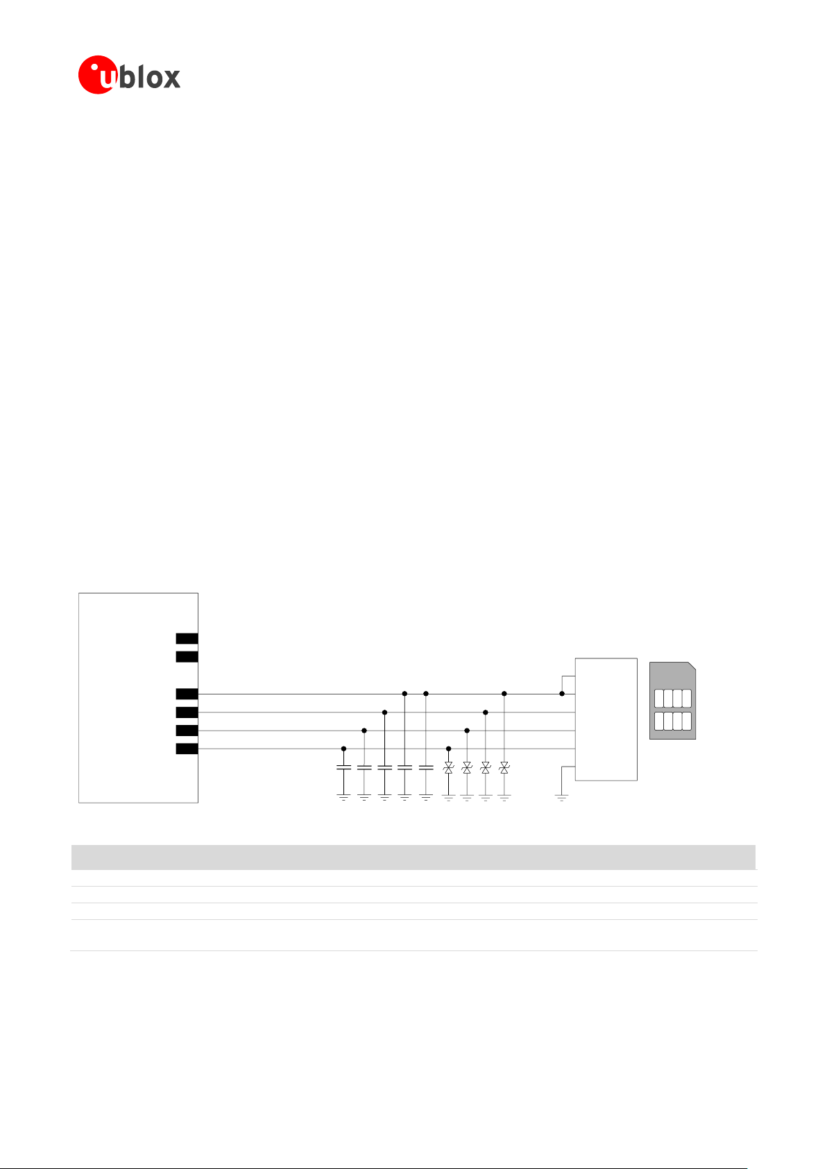
TOBY-L1 series - System Integration Manual
Please leave width at 16.9cm (17cm = .docx page width) to preserve 1:1 scaling
TOBY-L1 series
59
VSIM
57
SIM_IO
56
SIM_CLK
58
SIM_RST
4
V_INT
42
SIM CARD
HOLDER
C5C6C
7
C1C2C
3
SIM Card
Bottom View
(contacts side)
C
1
VPP (C6)
VCC (C1)
IO (C7)
CLK (C3)
RST (C2)
GND (C5)
C2C
3
C
5
J1
C
4
D1 D2 D3 D4
C
8
C
4
Reference
Description
Part Number - Manufacturer
C1, C2, C3, C4
47 pF Capacitor Ceramic C0G 0402 5% 50 V
GRM1555C1H470JA01 - Murata
C5
100 nF Capacitor Ceramic X7R 0402 10% 16 V
GRM155R71C104KA01 - Murata
D1, D2, D3, D4
Very Low Capacitance ESD Protection
PESD0402-140 - Tyco Electronics
J1
SIM Card Holder
6 positions, without card presence switch
Various Manufacturers,
C707 10M006 136 2 - Amphenol
Guidelines for single SIM card connection without detection
A removable SIM card placed in a SIM card holder must be connected the SIM card interface of TOBY-L1
modules as described in Figure 24, where the optional SIM detection feature is not implemented (refer to the
circuit described in Error! Reference source not found. if the SIM detection feature is not required).
Follow these guidelines connecting the module to a SIM connector without SIM presence detection:
Connect the UICC / SIM contacts C1 (VCC) and C6 (VPP) to the VSIM pin of the module
Connect the UICC / SIM contact C7 (I/O) to the SIM_IO pin of the module
Connect the UICC / SIM contact C3 (CLK) to the SIM_CLK pin of the module
Connect the UICC / SIM contact C2 (RST) to the SIM_RST pin of the module
Connect the UICC / SIM contact C5 (GND) to ground
Provide a 100 nF bypass capacitor (e.g. Murata GRM155R71C104K) at the SIM supply line (VSIM), close to
the relative pad of the SIM connector, to prevent digital noise
Provide a bypass capacitor of about 22 pF to 47 pF (e.g. Murata GRM1555C1H470J) on each SIM line
(VSIM, SIM_CLK, SIM_IO, SIM_RST), very close to each relative pad of the SIM connector, to prevent RF
coupling especially in case the RF antenna is placed closer than 10 - 30 cm from the SIM card holder
Provide a very low capacitance (i.e. less than 10 pF) ESD protection (e.g. Tyco Electronics PESD0402-140) on
each externally accessible SIM line, close to each relative pad of the SIM connector: ESD sensitivity rating of
the SIM interface pins is 1 kV (Human Body Model according to JESD22-A114), so that, according to the
EMC/ESD requirements of the custom application, higher protection level can be required if the lines are
externally accessible on the application device
Limit capacitance and series resistance on each SIM signal (SIM_CLK, SIM_IO, SIM_RST) to match the
requirements for the SIM interface (27.7 ns is the maximum allowed rise time on the SIM_CLK line, 1.0 µs is
the maximum allowed rise time on the SIM_IO and SIM_RST lines)
Figure 24: Application circuit for the connection to a single removable SIM card, with SIM detection not implemented
Table 16: Example of components for the connection to a single removable SIM card, with SIM detection not implemented
UBX-13001482 Objective Information Design-in
Page 51 of 85
Page 52

TOBY-L1 series - System Integration Manual
Please leave width at 16.9cm (17cm = .docx page width) to preserve 1:1 scaling
TOBY -L1 series
59
VSIM
57
SIM_IO
56
SIM_CLK
58
SIM_RST
4
V_INT
42
SIM CHIP
SIM Chip
Bottom View
(contacts side)C
1
VPP (C6)
VCC (C1)
IO (C7)
CLK (C3)
RST (C2)
GND (C5)
C2C
3
C
5
U
1
C
4
2
8
3
6
7
1
C1 C5
C2 C6
C3 C7
C4 C8
8
7
6
5
1
2
3
4
TP
Reference
Description
Part Number - Manufacturer
C1, C2, C3, C4
47 pF Capacitor Ceramic C0G 0402 5% 50 V
GRM1555C1H470JA01 - Murata
C5
100 nF Capacitor Ceramic X7R 0402 10% 16 V
GRM155R71C104KA01 - Murata
U1
SIM chip (M2M UICC Form Factor)
Various Manufacturers
Guidelines for single SIM chip connection
A solderable SIM chip (M2M UICC Form Factor) must be connected the SIM card interface of TOBY-L1 modules
as described in Figure 25, where the optional SIM detection feature is not implemented (refer to the circuit
described in Error! Reference source not found. if the SIM detection feature is not required).
Follow these guidelines connecting the module to a solderable SIM chip without SIM presence detection:
Connect the UICC / SIM contacts C1 (VCC) and C6 (VPP) to the VSIM pin of the module
Connect the UICC / SIM contact C7 (I/O) to the SIM_IO pin of the module
Connect the UICC / SIM contact C3 (CLK) to the SIM_CLK pin of the module
Connect the UICC / SIM contact C2 (RST) to the SIM_RST pin of the module
Connect the UICC / SIM contact C5 (GND) to ground
Provide a 100 nF bypass capacitor (e.g. Murata GRM155R71C104K) at the SIM supply line (VSIM) close to
the relative pad of the SIM chip, to prevent digital noise
Provide a bypass capacitor of about 22 pF to 47 pF (e.g. Murata GRM1555C1H470J) on each SIM line
(VSIM, SIM_CLK, SIM_IO, SIM_RST), to prevent RF coupling especially in case the RF antenna is placed
closer than 10 - 30 cm from the SIM card holder
Limit capacitance and series resistance on each SIM signal (SIM_CLK, SIM_IO, SIM_RST) to match the
requirements for the SIM interface (27.7 ns is the maximum allowed rise time on the SIM_CLK line, 1.0 µs is
the maximum allowed rise time on the SIM_IO and SIM_RST lines)
Figure 25: Application circuit for the connection to a single solderable SIM chip, with SIM detection not implemented
Table 17: Example of components for the connection to a single solderable SIM chip, with SIM detection not implemented
UBX-13001482 Objective Information Design-in
Page 52 of 85
Page 53

TOBY-L1 series - System Integration Manual
2.4.1.2 Guidelines for SIM layout design
The layout of the SIM card interface lines (VSIM, SIM_CLK, SIM_IO, SIM_RST) may be critical if the SIM card is
placed far away from the TOBY-L1 series modules or in close proximity to the RF antenna: these two cases
should be avoided or at least mitigated as described below.
In the first case, the long connection can cause the radiation of some harmonics of the digital data frequency as
any other digital interface: keep the traces short and avoid coupling with RF line or sensitive analog inputs.
In the second case, the same harmonics can be picked up and create self-interference that can reduce the
sensitivity of LTE receiver channels whose carrier frequency is coincidental with harmonic frequencies: placing the
RF bypass capacitors suggested in Error! Reference source not found. near the SIM connector will mitigate
the problem.
In addition, since the SIM card is typically accessed by the end user, it can be subjected to ESD discharges: add
adequate ESD protection as suggested in Error! Reference source not found. to protect module SIM pins near
the SIM connector.
Limit capacitance and series resistance on each SIM signal to match the SIM specifications: the connections
should always be kept as short as possible.
Avoid coupling with any sensitive analog circuit, since the SIM signals can cause the radiation of some harmonics
of the digital data frequency
UBX-13001482 Objective Information Design-in
Page 53 of 85
Page 54

TOBY-L1 series - System Integration Manual
TOBY-L1 series
D+
D-
GND
28
USB_D+
27
USB_D-
GND
USB DEVICE
CONNECTOR
D1 D2
Reference
Description
Part Number - Manufacturer
D1, D2
Very Low Capacitance ESD Protection
PESD0402-140 - Tyco Electronics
2.5 Serial interfaces
2.5.1 USB interface
2.5.1.1 Guidelines for USB circuit design
The USB_D+ and USB_D- lines carry the USB serial data and signaling. The lines are used in single ended mode
for full speed signaling handshake, as well as in differential mode for high speed signaling and data transfer.
USB pull-up or pull-down resistors on pins USB_D+ and USB_D- as required by the Universal Serial Bus Revision
2.0 specification [4] are part of the USB pad driver and do not need to be externally provided.
External series resistors on pins USB_D+ and USB_D- as required by the Universal Serial Bus Revision 2.0
specification [4] are also integrated and do not need to be externally provided.
Figure 26: USB Interface application circuit
Table 18: Component for USB application circuit
UBX-13001482 Objective Information Design-in
Page 54 of 85
Page 55

TOBY-L1 series - System Integration Manual
35 µm
35 µm
35 µm
35 µm
270 µm
270 µm
760 µm
L1 Copper
L3 Copper
L2 Copper
L4 Copper
FR-4 dielectric
FR-4 dielectric
FR-4 dielectric
350 µm 400 µm400 µm350 µm400 µm
35 µm
35 µm
1510 µm
L2 Copper
L1 Copper
FR-4 dielectric
740 µm 410 µm410 µm740 µm410 µm
2.5.1.2 Guidelines for USB layout design
The USB_D+ / USB_D- lines require accurate layout design to achieve reliable signaling at the high speed data
rate (up to 480 Mb/s) supported by the USB serial interface.
The characteristic impedance of the USB_D+ / USB_D- lines is specified by the Universal Serial Bus Revision 2.0
specification [4]. The most important parameter is the differential characteristic impedance applicable for the
odd-mode electromagnetic field, which should be as close as possible to 90 differential: signal integrity may
be degraded if PCB layout is not optimal, especially when the USB signaling lines are very long.
Use the following general routing guidelines to minimize signal quality problems:
Route USB_D+ / USB_D- lines as a differential pair
Route USB_D+ / USB_D- lines as short as possible
Ensure the differential characteristic impedance (Z
Ensure the common mode characteristic impedance (Z
) is as close as possible to 90
0
) is as close as possible to 30
CM
Consider design rules for USB_D+ / USB_D- similar to RF transmission lines, being them coupled differential
micro-strip or buried stripline: avoid any stubs, abrupt change of layout, and route on clear PCB area
Figure 27 and Figure 28 provide two examples of coplanar waveguide designs with differential characteristic
impedance close to 90 and common mode characteristic impedance close to 30 . The first transmission line
can be implemented in case of 4-layer PCB stack-up herein described, the second transmission line can be
implemented in case of 2-layer PCB stack-up herein described.
Figure 27: Example of USB line design, with Z0 close to 90 and ZCM close to 30 , for the described 4-layer board layup
Figure 28: Example of USB line design, with Z0 close to 90 and ZCM close to 30 , for the described 2-layer board layup
UBX-13001482 Objective Information Design-in
Page 55 of 85
Page 56

TOBY-L1 series - System Integration Manual
2.6 General Purpose Input/Output (GPIO)
2.6.1.1 Guidelines for GPIO circuit design
The following application circuits are suggested as general guideline for the usage of the GPIO pins available
with the TOBY-L1 modules, according to the relative custom function.
Network status indication:
The pin configured to provide the “Network status indication” function, e.g. the GPIO1, can be connected
on the application board to an input pin of an application processor or can drive a LED by a transistor with
integrated resistors to indicate network status.
UBX-13001482 Objective Information Design-in
Page 56 of 85
Page 57

TOBY-L1 series - System Integration Manual
2.7 Reserved pins (RSVD)
TOBY-L1 series modules have pins reserved for future use. All the RSVD pins are to be left unconnected on the
application board.
2.8 Module placement
Optimize placement for minimum length of RF line and closer path from DC source for VCC.
Make sure that RF and analog circuits are clearly separated from any other digital circuits on the system board.
Provide enough clearance between the module and any external part.
The heat dissipation during continuous transmission at maximum power can significantly raise the
temperature of the application base-board below the TOBY-L1 modules: avoid placing temperature
sensitive devices close to the module.
UBX-13001482 Objective Information Design-in
Page 57 of 85
Page 58
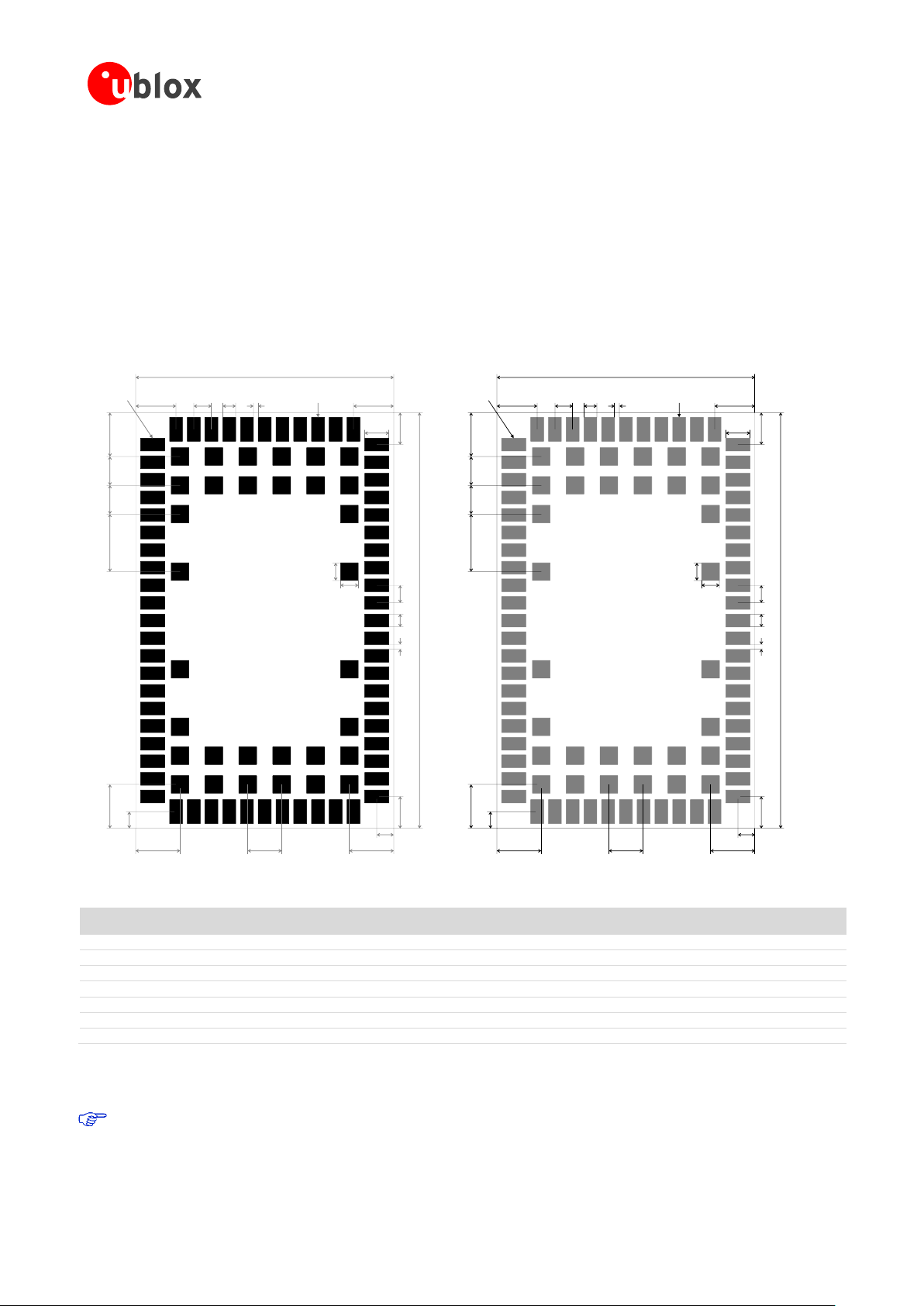
TOBY-L1 series - System Integration Manual
K
M1
M1
M2
E G H’ J’ E
ANT pin
B
Pin 1
K
G
H’
J’
A
D
D
O’
O’
L N L
I’
F’
F’
K
M1
M1
M2
E G H’’ J’’ E
ANT pin
B
Pin 1
K
G
H’’
J’’
A
D
D
O’’
O’’
L N L
I’’
F’’
F’’
Stencil: 150
µm
Parameter
Value
Parameter
Value
Parameter
Value
A
26.0 mm G
1.10 mm K
2.75 mm
B
16.0 mm H’
0.80 mm L
2.75 mm
C
3.00 mm H’’
0.75 mm M1
1.80 mm
D
2.00 mm I’
1.50 mm M2
3.60 mm
E
2.50 mm I’’
1.55 mm N
2.10 mm
F’
1.05 mm J’
0.30 mm O’
1.10 mm
F’’
1.00 mm J’’
0.35 mm O’’
1.05 mm
2.9 Module footprint and paste mask
Figure 29 and Table 19 describe the suggested footprint (i.e. copper mask) and paste mask layout for TOBY-L1
modules: the proposed land pattern layout reflects the modules’ pads layout, while the proposed stencil
apertures layout is slightly different (see the F’’, H’’, I’’, J’’, O’’ parameters compared to the F’, H’, I’, J’, O’ ones).
The Non Solder Mask Defined (NSMD) pad type is recommended over the Solder Mask Defined (SMD) pad type,
implementing the solder mask opening 50 µm larger per side than the corresponding copper pad.
The recommended solder paste thickness is 150 µm, according to application production process requirements.
Figure 29: TOBY-L1 series modules suggested footprint and paste mask (application board top view)
Table 19: TOBY-L1 series modules suggested footprint and paste mask dimensions
These are recommendations only and not specifications. The exact copper, solder and paste mask
geometries, distances, stencil thicknesses and solder paste volumes must be adapted to the specific
production processes (e.g. soldering etc.) of the customer.
UBX-13001482 Objective Information Design-in
Page 58 of 85
Page 59

TOBY-L1 series - System Integration Manual
UBX-13001482 Objective Information Design-in
Page 59 of 85
Page 60

TOBY-L1 series - System Integration Manual
1
2
3
2.10 Thermal guidelines
TOBY-L1 series module operating temperature range and module thermal resistance are specified in the
TOBY-L1 series Data Sheet [1].
The most critical condition concerning module thermal performance is the uplink transmission at maximum
power (data upload in connected-mode), when the baseband processor runs at full speed, radio circuits are all
active and the RF power amplifier is driven to higher output RF power. This scenario is not often encountered in
real networks; however the application should be correctly designed to cope with it.
During transmission at maximum RF power the TOBY-L1 series modules generate thermal power that can exceed
1 W: this is an indicative value since the exact generated power strictly depends on operating condition such as
the number of allocated TX slot, transmitting frequency band, etc. The generated thermal power must be
adequately dissipated through the thermal and mechanical design of the application.
The spreading of the Module-to-Ambient thermal resistance (Rth,M-A) depends on the module operating
condition. The overall temperature distribution is influenced by the configuration of the active components
during the specific mode of operation and their different thermal resistance toward the case interface.
Mounting a TOBY-L1 series module on a 79 mm x 62 mm x 1.41 mm 4-Layers PCB with a high coverage of
copper in still air conditions1, the increase of the module temperature2 in different modes of operation, referred
to idle state initial condition3, can be summarized as following:
~8 °C during a LTE connection (1 TX slot, 1 RX slot) at max TX power
~12 °C during a GPRS data transfer (2 TX slots, 3 RX slots) at max TX power
The Module-to-Ambient thermal resistance value and the relative increase of module temperature will be
different for other mechanical deployments of the module, e.g. PCB with different dimensions and
characteristics, mechanical shells enclosure, or forced air flow.
The increase of thermal dissipation, i.e. the Module-to-Ambient thermal resistance reduction, will decrease the
temperature for internal circuitry of TOBY-L1 series modules for a given operating ambient temperature. This
improves the device long-term reliability for applications operating at high ambient temperature.
A few hardware techniques may be used to reduce the Module-to-Ambient thermal resistance in the application:
Connect each GND pin with solid ground layer of the application board and connect each ground area of
the multilayer application board with complete thermal via stacked down to main ground layer.
Provide a ground plane as wide as possible on the application board.
Optimize antenna return loss, to optimize overall electrical performance of the module including a decrease
of module thermal power.
Optimize the thermal design of any high-power components included in the application, such as linear
regulators and amplifiers, to optimize overall temperature distribution in the application device.
Select the material, the thickness and the surface of the box (i.e. the mechanical enclosure of the application
device that integrates the module) so that it provides good thermal dissipation.
Force ventilation air-flow within mechanical enclosure.
Provide a heat sink component attached to the module top side, with electrically insulated / high thermal
conductivity adhesive, or on the backside of the application board, below the wireless module.
Refer to TOBY-L1 series Data Sheet [1] for the Rth,M-A value in this application condition
Temperature is measured by internal sensor of wireless module
Steady state thermal equilibrium is assumed. The module’s temperature in idle state can be considered equal to ambient temperature
UBX-13001482 Objective Information Design-in
Page 60 of 85
Page 61

TOBY-L1 series - System Integration Manual
For example, after the installation of a robust aluminum heat-sink with forced air ventilation on the back of the
same application board described above, the Module-to-Ambient thermal resistance (Rth,M-A) is reduced up to
the Module-to-Case thermal resistance (Rth,M-C) defined in the TOBY-L1 series Data Sheet [1]. The effect of
lower Rth,M-A can be seen from the module temperature increase, which now can be summarized as following:
~1 °C during a LTE connection (1 TX slot, 1 RX slot) at the maximum TX power
Beside the reduction of the Module-to-Ambient thermal resistance implemented by the hardware design of the
application device integrating a TOBY-L1 series module, the increase of module temperature can be moderated
by the software implementation of the application.
Since the most critical condition concerning module thermal power occurs when module connected-mode is
enabled, the actual module thermal power depends, as module current consumption, on the radio access
mode,the operating band and the average TX power.
UBX-13001482 Objective Information Design-in
Page 61 of 85
Page 62

TOBY-L1 series - System Integration Manual
Application
Category
Immunity Level
All exposed surfaces of the radio equipment and ancillary equipment in a
representative configuration
Contact Discharge
4 kV
Air Discharge
8 kV
2.11 ESD guidelines
2.11.1 ESD immunity test overview
The immunity of devices integrating TOBY-L1 series modules to Electro-Static Discharge (ESD) is part of the
Electro-Magnetic Compatibility (EMC) conformity which is required for products bearing the CE marking,
compliant with the R&TTE Directive (99/5/EC), the EMC Directive (89/336/EEC) and the Low Voltage Directive
(73/23/EEC) issued by the Commission of the European Community.
Compliance with these directives implies conformity to the following European Norms for device ESD immunity:
ESD testing standard CENELEC EN 61000-4-2 [6] and the radio equipment standards ETSI EN 301 489-1 [7], ETSI
EN 301 489-7 [8], ETSI EN 301 489-24 [9], which requirements are summarized in Table 20.
The ESD immunity test is performed at the enclosure port, defined by ETSI EN 301 489-1 [7] as the physical
boundary through which the electromagnetic field radiates. If the device implements an integral antenna, the
enclosure port is seen as all insulating and conductive surfaces housing the device. If the device implements a
removable antenna, the antenna port can be separated from the enclosure port. The antenna port includes the
antenna element and its interconnecting cable surfaces.
The applicability of ESD immunity test to the whole device depends on the device classification as defined by ETSI
EN 301 489-1 [7]. Applicability of ESD immunity test to the relative device ports or the relative intercon necting
cables to auxiliary equipment, depends on device accessible interfaces and manufacturer requirements, as
defined by ETSI EN 301 489-1 [7].
Contact discharges are performed at conductive surfaces, while air discharges are performed at insulating
surfaces. Indirect contact discharges are performed on the measurement setup horizontal and vertical coupling
planes as defined in CENELEC EN 61000-4-2 [6].
For the definition of integral antenna, removable antenna, antenna port, device classification refer to ETSI
EN 301 489-1 [7].
CENELEC EN 61000-4-2 [6] defines the contact and air discharges.
Table 20: Electro-Magnetic Compatibility ESD immunity requirements as defined by CENELEC EN 61000-4-2, ETSI EN 301 489-1,
ETSI EN 301 489-7, ETSI EN 301 489-24
2.11.2 ESD immunity test of TOBY-L1 series reference designs
Although Electro-Magnetic Compatibility (EMC) certification is required for customized devices integrating
TOBY-L1 series modules for R&TTED and European Conformance CE mark, EMC certification (including ESD
immunity) has been successfully performed on TOBY-L1 series modules reference design according to CENELEC
EN 61000-4-2 [6], ETSI EN 301 489-1 [7], ETSI EN 301 489-7 [8], ETSI EN 301 489-24 [9] European Norms.
The EMC / ESD approved u-blox reference designs consist of a TOBY-L1 series module soldered onto a
motherboard which provides supply interface, SIM card, headset and communication port. An external antenna
is connected to an SMA connector provided on the motherboard for the LTE antenna.
Since an external antenna is used, the antenna port can be separated from the enclosure port. The reference
design is not enclosed in a box so that the enclosure port is not identified with physical surfaces. Therefore,
some test cases cannot be applied. Only the antenna port is identified as accessible for direct ESD exposure.
UBX-13001482 Objective Information Design-in
Page 62 of 85
Page 63

TOBY-L1 series - System Integration Manual
Category
Application
Immunity Level
Remarks
Contact Discharge
to coupling planes
(indirect contact discharge)
Enclosure
+4 kV / -4 kV
Contact Discharges
to conducted surfaces
(direct contact discharge)
Enclosure port
Not Applicable
Test not applicable to u-blox reference design because it
does not provide enclosure surface.
The test is applicable only to equipment providing
conductive enclosure surface.
Antenna port
+4 kV / -4 kV
Test applicable to u-blox reference design because it
provides antenna with conductive & insulating surfaces.
The test is applicable only to equipment providing
antenna with conductive surface.
Air Discharge
at insulating surfaces
Enclosure port
Not Applicable
Test not applicable to the u-blox reference design
because it does not provide an enclosure surface.
The test is applicable only to equipment providing
insulating enclosure surface.
Antenna port
+8 kV / -8 kV
Test applicable to u-blox reference design because it
provides antenna with conductive & insulating surfaces.
The test is applicable only to equipment providing
antenna with insulating surface.
u-blox TOBY-L1 series reference design implement all the ESD precautions described in section 2.11.3.
Table 21 reports the u-blox TOBY-L1 series reference designs ESD immunity test results, according to test
requirements stated in the CENELEC EN 61000-4-2 [6], ETSI EN 301 489-1 [7], ETSI EN 301 489-7 [8] and ETSI
EN 301 489-24 [9].
Table 21: Enclosure ESD immunity level of u-blox TOBY-L1 series modules reference designs
2.11.3 ESD application circuits
The application circuits described in this section are recommended and should be implemented in the device
integrating TOBY-L1 series modules, according to the application board classification (see
ETSI EN 301 489-1 [7]), to satisfy the requirements for ESD immunity test summarized in Table 20.
Antenna interface
The ANT pin of TOBY-L1 series modules provides ESD immunity up to ±4 kV for direct Contact Discharge and up
to ±8 kV for Air Discharge: no further precaution to ESD immunity test is needed, as implemented in the EMC /
ESD approved reference design of TOBY-L1 series modules.
The antenna interface application circuit implemented in the EMC / ESD approved reference designs of TOBY-L1
series modules is described in Figure 23
RESET_N pin
The following precautions are suggested for the RESET_N line of TOBY-L1 series modules, depending on the
application board handling, to satisfy ESD immunity test requirements:
It is recommended to keep the connection line to RESET_N as short as possible
UBX-13001482 Objective Information Design-in
Page 63 of 85
Page 64

TOBY-L1 series - System Integration Manual
Maximum ESD sensitivity rating of the RESET_N pin is 1 kV (Human Body Model according to JESD22-A114).
Higher protection level could be required if the RESET_N pin is externally accessible on the application board.
The following precautions are suggested to achieve higher protection level:
A general purpose ESD protection device (e.g. EPCOS CA05P4S14THSG varistor array or EPCOS
CT0402S14AHSG varistor) should be mounted on the RESET_N line, close to accessible point
The RESET_N application circuit implemented in the EMC / ESD approved reference designs of TOBY-L1 series
modules is described in Figure 19 and Table 15 (section 2.2.2).
SIM interface
The following precautions are suggested for TOBY-L1 series modules SIM interface (VSIM, SIM_RST, SIM_IO,
SIM_CLK pins), depending on the application board handling, to satisfy ESD immunity test requirements:
A 47 pF bypass capacitor (e.g. Murata GRM1555C1H470J) must be mounted on the lines connected to
VSIM, SIM_RST, SIM_IO and SIM_CLK pins to assure SIM interface functionality when an electrostatic
discharge is applied to the application board enclosure
It is suggested to use as short as possible connection lines at SIM pins
Maximum ESD sensitivity rating of SIM interface pins is 1 kV (Human Body Model according to JESD22-A114).
Higher protection level could be required if SIM interface pins are externally accessible on the application board.
The following precautions are suggested to achieve higher protection level:
A low capacitance (i.e. less than 10 pF) ESD protection device (e.g. Tyco Electronics PESD0402-140) should
be mounted on each SIM interface line, close to accessible points (i.e. close to the SIM card holder)
The SIM interface application circuit implemented in the EMC / ESD approved reference designs of TOBY-L1
series modules is described in Error! Reference source not found. and Error! Reference source not found.
(section 2.4).
Other pins and interfaces
All the module pins that are externally accessible on the device integrating TOBY-L1 series module should be
included in the ESD immunity test since they are considered to be a port as defined in ETSI EN 301 489-1 [7].
Depending on applicability, to satisfy ESD immunity test requirements according to ESD category level, all the
module pins that are externally accessible should be protected up to ±4 kV for direct Contact Discharge and up
to ±8 kV for Air Discharge applied to the enclosure surface.
The maximum ESD sensitivity rating of all the other pins of the module is 1 kV (Human Body Model according to
JESD22-A114). Higher protection level could be required if the relative pin is externally accessible on the
application board. The following precautions are suggested to achieve higher protection level:
A general purpose ESD protection device (e.g. EPCOS CA05P4S14THSG or EPCOS CT0402S14AHSG varistor)
should be mounted on the relative line, close to accessible point
UBX-13001482 Objective Information Design-in
Page 64 of 85
Page 65
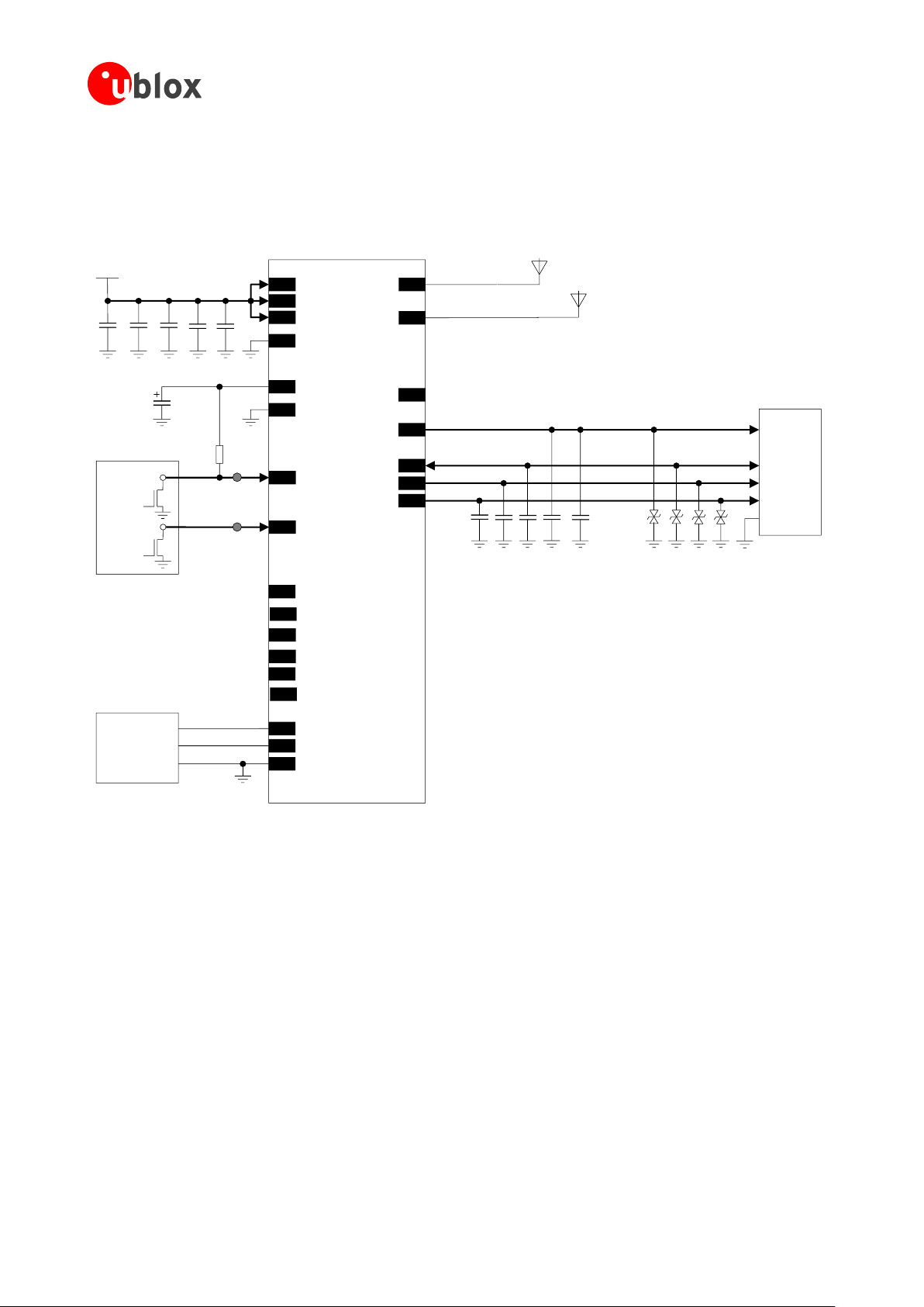
TOBY-L1 series - System Integration Manual
Please leave width at 16.9cm (17cm = .docx page width) to preserve 1:1 scaling
3V8
GND
330µF
10nF100nF 56pF
TOBY-L100
71 VCC
72 VCC
70 VCC
+
100µF
3
V_BCK
P
GND GND
GND
RTC
back-up
USB
21 GPIO1
23 RESET_N
Application
Processor
Open
Drain
Output
20 PWR_ON
100kΩ
Open
Drain
Output
D-
D+
29 D-
28 D+
GPIO3
GPIO4
24
25
GPIO2
22
15pF
60 GPIO5
61 GPIO6
47pF
SIM Card
VCC
IO
CLK
RST
GND
47pF 47pF 100nF
59VSIM
57
SIM_IO
56
SIM_CLK
58
SIM_RST
47pF
5V_INT
ESD ESD ESD ESD
81
ANT1
82ANT2
External
Antennas
TP
TP
2.12 Schematic for TOBY-L1 series module integration
Figure 30 is an example of a schematic diagram where a TOBY-L100 module is integrated into an application
board, using all the available interfaces and functions of the module.
Figure 30: Example of schematic diagram to integrate TOBY-L100 module in an application board, using all the interfaces
UBX-13001482 Objective Information Design-in
Page 65 of 85
Page 66

TOBY-L1 series - System Integration Manual
UBX-13001482 Objective Information Design-in
Page 66 of 85
Page 67

TOBY-L1 series - System Integration Manual
2.13 Design-in checklist
This section provides a design-in checklist.
2.13.1 Schematic checklist
The following are the most important points for a simple schematic check:
DC supply must provide a nominal voltage at VCC pin above the minimum operating range limit.
DC supply must be capable of providing 1.0 A current pulses, providing a voltage at VCC pin above the
minimum operating range limit and with a maximum 400 mV voltage drop from the nominal value.
VCC supply should be clean, with very low ripple/noise: provide the suggested bypass capacitors, in
particular if the application device integrates an internal antenna.
Do not leave PWR_ON floating: fix properly the level, e.g. adding a proper pull-up resistor to V_BCKP.
Do not apply loads which might exceed the limit for maximum available current from V_INT supply.
Check that voltage level of any connected pin does not exceed the relative operating range.
Capacitance and series resistance must be limited on each SIM signal to match the SIM specifications.
Insert the suggested capacitors on each SIM signal and low capacitance ESD protections if accessible.
Provide accessible testpoints directly connected to the following pins: V_INT pin, PWR_ON and/or
RESET_N pins, to allow the module firmware upgrade using the u-blox EasyFlash tool and to allow the
trace log capture (debug purpose).
Provide proper precautions for ESD immunity as required on the application board.
All unused pins can be left unconnected except the PWR_ON pin (its level must be properly fixed, e.g.
adding a 100 k pull-up to V_BCKP).
UBX-13001482 Objective Information Design-in
Page 67 of 85
Page 68

TOBY-L1 series - System Integration Manual
2.13.2 Layout checklist
The following are the most important points for a simple layout check:
Check 50 nominal characteristic impedance of the RF transmission line connected to the ANT pad
(antenna RF input/output interface).
Ensure no coupling occurs between the RF interface and noisy or sensitive signals (primarily analog audio
input/output signals, SIM signals, high-speed digital lines).
VCC line should be wide and short.
Route VCC supply line away from sensitive analog signals.
Ensure proper grounding.
Optimize placement for minimum length of RF line and closer path from DC source for VCC.
Keep routing short and minimize parasitic capacitance on the SIM lines to preserve signal integrity.
2.13.3 Antenna checklist
Antenna termination should provide 50 characteristic impedance with V.S.W.R at least less than 3:1
(recommended 2:1) on operating bands in deployment geographical area.
Follow the recommendations of the antenna producer for correct antenna installation and deployment
(PCB layout and matching circuitry).
Follow the additional guidelines for products marked with the FCC logo (United States only) reported in
chapter 2.3.1.2 and 4.2.2
Follow the guidelinesError! Reference source not found. to get proper antenna detection
functionality, if required.
UBX-13001482 Objective Information Design-in
Page 68 of 85
Page 69

TOBY-L1 series - System Integration Manual
3 Handling and soldering
No natural rubbers, no hygroscopic materials or materials containing asbestos are employed.
3.1 Packaging, shipping, storage and moisture preconditioning
For information pertaining to reels and tapes, Moisture Sensitivity levels (MSD), shipment and storage
information, as well as drying for preconditioning see the TOBY-L1 series Data Sheet [1] and the u-blox Package
Information Guide Error! Reference source not found..
The TOBY-L1 series modules are Electro-Static Discharge (ESD) sensitive devices.
Ensure ESD precautions are implemented during handling of the module.
3.2 Soldering
3.2.1 Soldering paste
Use of "No Clean" soldering paste is strongly recommended, as it does not require cleaning after the soldering
process has taken place. The paste listed in the example below meets these criteria.
Soldering Paste: OM338 SAC405 / Nr.143714 (Cookson Electronics)
Alloy specification: 95.5% Sn / 3.9% Ag / 0.6% Cu (95.5% Tin / 3.9% Silver / 0.6% Copper)
95.5% Sn / 4.0% Ag / 0.5% Cu (95.5% Tin / 4.0% Silver / 0.5% Copper)
Melting Temperature: 217 °C
Stencil Thickness: 150 µm for base boards
The final choice of the soldering paste depends on the approved manufacturing procedures.
The paste-mask geometry for applying soldering paste should meet the recommendations in section 2.9
The quality of the solder joints on the connectors (’half vias’) should meet the appropriate IPC
specification.
3.2.2 Reflow soldering
A convection type-soldering oven is strongly recommended over the infrared type radiation oven.
Convection heated ovens allow precise control of the temperature and all parts will be heated up evenly,
regardless of material properties, thickness of components and surface color.
Consider the "IPC-7530 Guidelines for temperature profiling for mass soldering (reflow and wave) processes,
published 2001".
Reflow profiles are to be selected according to the following recommendations.
Failure to observe these recommendations can result in severe damage to the device!
UBX-13001482 Objective Information Handling and soldering
Page 69 of 85
Page 70

TOBY-L1 series - System Integration Manual
Prehea t Heating Cooling
[°C] Peak T emp. 245°C [°C]
250 250
Liquidus Te mperature
217 217
200 200
40 - 60 s
End Temp.
max 4°C/s
150 - 200°C
150 150
max 3°C/s
60 - 120 s
100 Typical Le adfre e 100
Soldering Profile
50 50
Elapsed time [s ]
Preheat phase
Initial heating of component leads and balls. Residual humidity will be dried out. Note that this preheat phase
will not replace prior baking procedures.
Temperature rise rate: max 3 °C/s If the temperature rise is too rapid in the preheat phase it may cause
excessive slumping.
Time: 60 – 120 s If the preheat is insufficient, rather large solder balls tend to be
generated. Conversely, if performed excessively, fine balls and large
balls will be generated in clusters.
End Temperature: 150 - 200 °C If the temperature is too low, non-melting tends to be caused in
areas containing large heat capacity.
Heating/ reflow phase
The temperature rises above the liquidus temperature of 217 °C. Avoid a sudden rise in temperature as the
slump of the paste could become worse.
Limit time above 217 °C liquidus temperature: 40 - 60 s
Peak reflow temperature: 245 °C
Cooling phase
A controlled cooling avoids negative metallurgical effects (solder becomes more brittle) of the solder and
possible mechanical tensions in the products. Controlled cooling helps to achieve bright solder fillets with a good
shape and low contact angle.
Temperature fall rate: max 4 °C/s
To avoid falling off, modules should be placed on the topside of the motherboard during soldering.
The soldering temperature profile chosen at the factory depends on additional external factors like choice of
soldering paste, size, thickness and properties of the base board, etc.
Exceeding the maximum soldering temperature and the maximum liquidus time limit in the
recommended soldering profile may permanently damage the module.
Figure 31: Recommended soldering profile
TOBY-L1 series modules must not be soldered with a damp heat process.
UBX-13001482 Objective Information Handling and soldering
Page 70 of 85
Page 71

TOBY-L1 series - System Integration Manual
3.2.3 Optical inspection
After soldering the TOBY-L1 series modules, inspect the modules optically to verify that the module is properly
aligned and centered.
3.2.4 Cleaning
Cleaning the soldered modules is not recommended. Residues underneath the modules cannot be easily
removed with a washing process.
Cleaning with water will lead to capillary effects where water is absorbed in the gap between the baseboard
and the module. The combination of residues of soldering flux and encapsulated water leads to short circuits
or resistor-like interconnections between neighboring pads. Water will also damage the sticker and the inkjet printed text.
Cleaning with alcohol or other organic solvents can result in soldering flux residues flooding into the two
housings, areas that are not accessible for post-wash inspections. The solvent will also damage the sticker
and the ink-jet printed text.
Ultrasonic cleaning will permanently damage the module, in particular the quartz oscillators.
For best results use a "no clean" soldering paste and eliminate the cleaning step after the soldering.
3.2.5 Repeated reflow soldering
Only a single reflow soldering process is encouraged for boards with a TOBY-L1 series module populated on it.
The reason for this is the risk of the module falling off due to high weight in relation to the adhesive properties
of the solder.
3.2.6 Wave soldering
Boards with combined through-hole technology (THT) components and surface-mount technology (SMT) devices
require wave soldering to solder the THT components. Only a single wave soldering process is encouraged for
boards populated with TOBY-L1 series modules.
3.2.7 Hand soldering
Hand soldering is not recommended.
3.2.8 Rework
Rework is not recommended.
Never attempt a rework on the module itself, e.g. replacing individual components. Such actions
immediately terminate the warranty.
3.2.9 Conformal coating
Certain applications employ a conformal coating of the PCB using HumiSeal® or other related coating products.
These materials affect the HF properties of the TOBY-L1 series modules and it is important to prevent them from
flowing into the module.
The RF shields do not provide 100% protection for the module from coating liquids with low viscosity, therefore
care is required in applying the coating.
Conformal Coating of the module will void the warranty.
UBX-13001482 Objective Information Handling and soldering
Page 71 of 85
Page 72

TOBY-L1 series - System Integration Manual
3.2.10 Casting
If casting is required, use viscose or another type of silicon pottant. The OEM is strongly advised to qualify such
processes in combination with the TOBY-L1 series modules before implementing this in the production.
Casting will void the warranty.
3.2.11 Grounding metal covers
Attempts to improve grounding by soldering ground cables, wick or other forms of metal strips directly onto the
EMI covers is done at the customer's own risk. The numerous ground pins should be sufficient to provide
optimum immunity to interferences and noise.
u-blox gives no warranty for damages to the TOBY-L1 series modules caused by soldering metal cables or
any other forms of metal strips directly onto the EMI covers.
3.2.12 Use of ultrasonic processes
TOBY-L1 series modules contain components which are sensitive to Ultrasonic Waves. Use of any Ultrasonic
Processes (cleaning, welding etc.) may cause damage to the module.
u-blox gives no warranty against damages to the TOBY-L1 series modules caused by any Ultrasonic
Processes.
UBX-13001482 Objective Information Handling and soldering
Page 72 of 85
Page 73

TOBY-L1 series - System Integration Manual
4 Approvals
For the complete list of all the certification schemes approvals of TOBY-L1 series modules and the
corresponding declarations of conformity, refer to the u-blox web-site (http://www.u-blox.com).
4.1 Product certification approval overview
Product certification approval is the process of certifying that a product has passed all tests and criteria required
by specifications, typically called “certification schemes” that can be divided into three distinct categories:
Regulatory certification
o Country specific approval required by local government in most regions and countries, as:
CE (Conformité Européenne) marking for European Union
FCC (Federal Communications Commission) approval for United States
Industry certification
o Telecom industry specific approval verifying the interoperability between devices and networks:
GCF (Global Certification Forum), partnership between European device manufacturers and
network operators to ensure and verify global interoperability between devices and networks
PTCRB (PCS Type Certification Review Board), created by United States network operators to
ensure and verify interoperability between devices and North America networks
Operator certification
o Operator specific approval required by some mobile network operator, as:
AT&T network operator in United States
Even if TOBY-L1 modules are approved under all major certification schemes, the application device that
integrates TOBY-L1 modules must be approved under all the certification schemes required by the specific
application device to be deployed in the market.
The required certification scheme approvals and relative testing specifications differ depending on the country or
the region where the device that integrates TOBY-L1 series modules must be deployed, on the relative vertical
market of the device, on type, features and functionalities of the whole application device, and on the network
operators where the device must operate.
The certification of the application device that integrates a TOBY-L1 module and the compliance of the
application device with all the applicable certification schemes, directives and standards are the sole
responsibility of the application device manufacturer.
TOBY-L1 modules are certified according to all capabilities and options stated in the Protocol Implementation
Conformance Statement document (PICS) of the module. The PICS, according to 3GPP TS 51.010-2 [5], is a
statement of the implemented and supported capabilities and options of a device.
The PICS document of the application device integrating a TOBY-L1 module must be updated from the
module PICS statement if any feature stated as supported by the module in its PICS document is not
implemented or disabled in the application device, as for the following cases:
UBX-13001482 Objective Information Approvals
Page 73 of 85
o if the automatic network attach is disabled by AT+COPS command
Page 74

TOBY-L1 series - System Integration Manual
4.2 Federal Communications Commission and Industry Canada notice
Federal Communications Commission (FCC) ID:
R5Q-TOBYL100
Industry Canada (IC) Certification Number:
8595A-TOBYL100
4.2.1 Safety Warnings review the structure
Equipment for building-in. The requirements for fire enclosure must be evaluated in the end product
The clearance and creepage current distances required by the end product must be withheld when the
module is installed
The cooling of the end product shall not negatively be influenced by the installation of the module
Excessive sound pressure from earphones and headphones can cause hearing loss
No natural rubbers, no hygroscopic materials nor materials containing asbestos are employed
4.2.2 Declaration of Conformity – United States only
This device complies with Part 27 of the FCC rules. Operation is subject to the following two conditions:
this device may not cause harmful interference
this device must accept any interference received, including interference that may cause undesired operation
Radiofrequency radiation exposure Information: this equipment complies with FCC radiation
exposure limits prescribed for an uncontrolled environment for fixed and mobile use conditions.
This equipment should be installed and operated with a minimum distance of 20 cm between
the radiator and the body of the user or nearby persons. This transmitter must not be colocated or operating in conjunction with any other antenna or transmitter except as authorized
in the certification of the product.
The gain of the system antenna(s) used for the TOBY-L1 series modules (i.e. the combined
transmission line, connector, cable losses and radiating element gain) must not exceed 10.7 dBi
(for LTE band 13) and 6.57 dBi (for LTE band 4) for mobile and fixed or mobile operating
configurations.
4.2.3 Modifications
The FCC requires the user to be notified that any changes or modifications made to this device that are not
expressly approved by u-blox could void the user's authority to operate the equipment.
Manufacturers of mobile or fixed devices incorporating the TOBY-L1 series modules are
authorized to use the FCC Grants and Industry Canada Certificates of the TOBY-L1 series
modules for their own final products according to the conditions referenced in the certificates.
The FCC Label shall in the above case be visible from the outside, or the host device shall bear a
second label stating:
"Contains FCC ID: R5Q-TOBYL100" resp.
The IC Label shall in the above case be visible from the outside, or the host device shall bear a
second label stating:
"Contains IC: 8595A-TOBYL100" resp.
Canada, Industry Canada (IC) Notices
This Class B digital apparatus complies with Canadian ICES-003 and RSS-210.
Operation is subject to the following two conditions:
UBX-13001482 Objective Information Approvals
Page 74 of 85
Page 75

TOBY-L1 series - System Integration Manual
o this device may not cause interference
o this device must accept any interference, including interference that may cause undesired
operation of the device
Radio Frequency (RF) Exposure Information
The radiated output power of the u-blox Wireless Module is below the Industry Canada (IC)
radio frequency exposure limits. The u-blox Wireless Module should be used in such a manner
such that the potential for human contact during normal operation is minimized.
This device has been evaluated and shown compliant with the IC RF Exposure limits under
mobile exposure conditions (antennas are greater than 20cm from a person's body).
This device has been certified for use in Canada. Status of the listing in the Industry Canada’s
REL (Radio Equipment List) can be found at the following web address:
http://www.ic.gc.ca/app/sitt/reltel/srch/nwRdSrch.do?lang=eng
Additional Canadian information on RF exposure also can be found at the following web
address: http://www.ic.gc.ca/eic/site/smt-gst.nsf/eng/sf08792.html
IMPORTANT: Manufacturers of portable applications incorporating the TOBY-L1 series modules
are required to have their final product certified and apply for their own FCC Grant and Industry
Canada Certificate related to the specific portable device. This is mandatory to meet the SAR
requirements for portable devices.
Changes or modifications not expressly approved by the party responsible for compliance
could void the user's authority to operate the equipment.
Canada, avis d'Industrie Canada (IC)
Cet appareil numérique de classe B est conforme aux normes canadiennes ICES-003 et RSS-139.
Son fonctionnement est soumis aux deux conditions suivantes:
o cet appareil ne doit pas causer d'interférence
o cet appareil doit accepter toute interférence, notamment les interférences qui peuvent
affecter son fonctionnement
Informations concernant l'exposition aux fréquences radio (RF)
La puissance de sortie émise par l’appareil de sans fil u-blox Wireless Module est inférieure à
la limite d'exposition aux fréquences radio d'Industrie Canada (IC). Utilisez l’appareil de sans
fil u-blox Wireless Module de façon à minimiser les contacts humains lors du fonctionnement
normal.
Ce périphérique a été évalué et démontré conforme aux limites d'exposition aux fréquences
radio (RF) d'IC lorsqu'il est installé dans des produits hôtes particuliers qui fonctionnent dans
des conditions d'exposition à des appareils mobiles (les antennes se situent à plus de 20
centimètres du corps d'une personne).
Ce périphérique est homologué pour l'utilisation au Canada. Pour consulter l'entrée
correspondant à l’appareil dans la liste d'équipement radio (REL - Radio Equipment List)
d'Industrie Canada rendez-vous sur:
http://www.ic.gc.ca/app/sitt/reltel/srch/nwRdSrch.do?lang=fra
Pour des informations supplémentaires concernant l'exposition aux RF au Canada rendez-vous
sur: http://www.ic.gc.ca/eic/site/smt-gst.nsf/eng/sf08792.html
IMPORTANT: les fabricants d'applications portables contenant les modules TOBY-L1 series
doivent faire certifier leur produit final et déposer directement leur candidature pour une
certification FCC ainsi que pour un certificat Industrie Canada délivré par l'organisme chargé de
ce type d'appareil portable. Ceci est obligatoire afin d'être en accord avec les exigences SAR
pour les appareils portables.
Tout changement ou modification non expressément approuvé par la partie responsable de la
certification peut annuler le droit d'utiliser l'équipement.
UBX-13001482 Objective Information Approvals
Page 75 of 85
Page 76

TOBY-L1 series - System Integration Manual
1909
4.3 R&TTED and European Conformance CE mark
This device has been evaluated against the essential requirements of the 1999/5/EC Directive.
In order to satisfy the essential requirements of 1999/5/EC Directive, the module is compliant with the following
standards:
Radio Frequency spectrum use (R&TTE art. 3.2):
o EN 301 511 V9.0.2
Electromagnetic Compatibility (R&TTE art. 3.1b):
o EN 301 489-1 V1.9.2
o EN 301 489-7 V1.4.1
Health and Safety (R&TTE art. 3.1a)
o EN 60950-1:2006 + A11:2009 + A1:2010 + A12:2011 + AC:2011
o EN 62311:2008
The conformity assessment procedure referred to in Article 10 and detailed in Annex IV of Directive 1999/5/EC
has been followed with the involvement of the following Notified Body No: 1909
Thus, the following marking is included in the product:
There is no restriction for the commercialisation of this device in all the countries of the European Union.
UBX-13001482 Objective Information Approvals
Page 76 of 85
Page 77
TOBY-L1 series - System Integration Manual
5 Product Testing
5.1 u-blox in-series production test
u-blox focuses on high quality for its products. All units produced are fully tested. Defective units are analyzed in
detail to improve the production quality.
This is achieved with automatic test equipment, which delivers a detailed test report for each unit. The following
measurements are done:
Digital self-test (firmware download, Flash firmware verification, IMEI programming)
Measurement of voltages and currents
Adjustment of ADC measurement interfaces
Functional tests (USB interface communication, SIM card communication)
Digital tests (GPIOs)
Measurement and calibration of RF characteristics in all supported bands (Receiver S/N verification, frequency
tuning of reference clock, calibration of transmitter and receiver power levels)
Verification of RF characteristics after calibration (modulation accuracy, power levels and spectrum
performance are checked to be within tolerances when calibration parameters are applied)
Figure 32: Automatic test equipment for module tests
5.2 Test parameters for OEM manufacturer
Because of the testing done by u-blox (with 100% coverage), an OEM manufacturer does not need to repeat
firmware tests or measurements of the module RF performance or tests over analog and digital interfaces in their
production test.
An OEM manufacturer should focus on:
Module assembly on the device; it should be verified that:
o Soldering and handling process did not damaged the module components
o All module pins are well soldered on device board
o There are no short circuits between pins
UBX-13001482 Objective Information Product Testing
Page 77 of 85
Page 78

TOBY-L1 series - System Integration Manual
Component assembly on the device; it should be verified that:
o Communication with host controller can be established
o The interfaces between module and device are working
o Overall RF performance test of the device including antenna
Dedicated tests can be implemented to check the device. For example, the measurement of module current
consumption when set in a specified status can detect a short circuit if compared with a “Golden Device” result.
Module AT commands are used to perform functional tests (communication with host controller, check SIM card
interface, check communication between module and GPIOs, etc.) and to perform RF performance tests.
5.2.1 “Go/No go” tests for integrated devices
A ‘Go/No go’ test is to compare the signal quality with a “Golden Device” in a position with excellent network
coverage and after having established a data connection (refer to TOBY-L1xx AT Commands Manual [2],
AT+CSQ command: <rssi>, <ber> parameters).
These kinds of test may be useful as a ‘go/no go’ test but not for RF performance measurements.
This test is suitable to check the communication with host controller and SIM card, the audio and power supply
functionality and verify if components at antenna interface are well soldered.
5.2.2 Functional tests providing RF operation
Overall RF performance test of the device including antenna can be performed with basic instruments such as a
spectrum analyzer (or an RF power meter) and a signal generator using AT+UTEST command over AT interface.
The AT+UTEST command gives a simple interface to set the module to Rx and Tx test modes ignoring LTE
signaling protocol. The command can set the module:
In transmitting mode in a specified channel and power level in all supported modulation schemes (single slot
GMSK) and bands
In receiving mode in a specified channel to returns the measured power level in all supported bands
Refer to the TOBY-L1xx AT Commands Manual [2], for AT+UTEST command syntax description.
Refer to the End user test Application Note Error! Reference source not found., for AT+UTEST
command user guide, limitations and examples of use.
UBX-13001482 Objective Information Product Testing
Page 78 of 85
Page 79
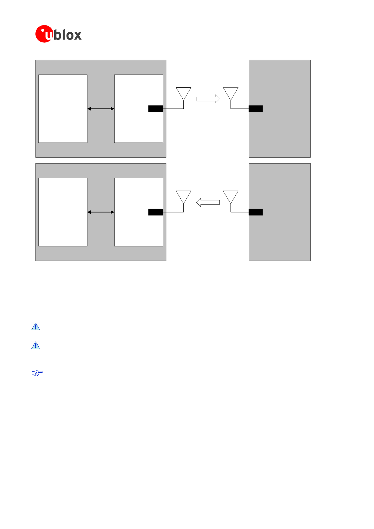
TOBY-L1 series - System Integration Manual
Application Board
TOBY-L1
series
ANT
Application
Processor
AT
Commands
Wireless
Antenna
Spectrum
Analyzer
IN
Wideband
Antenna
TX
Application Board
TOBY-L1
series
ANT
Application
Processor
AT
Commands
Wireless
Antenna
Signal
Generetor
OUT
Wideband
Antenna
RX
Figure 33: Setup with spectrum analyzer and signal generator for radiated measurement
This feature allows the measurement of the transmitter and receiver power levels to check component assembly
related to the module antenna interface and to check other device interfaces from which depends the RF
performance.
To avoid module damage during transmitter test, a proper antenna according to module
specifications or a 50 termination must be connected to ANT pin.
To avoid module damage during receiver test the maximum power level received at ANT pin
must meet module specifications.
The AT+UTEST command sets the module to emit RF power ignoring LTE signalling protocol. This emission
can generate interference that can be prohibited by law in some countries. The use of this feature is
intended for testing purpose in controlled environments by qualified user and must not be used during
the normal module operation. Follow instructions suggested in u-blox documentation. u-blox assumes no
responsibilities for the inappropriate use of this feature.
UBX-13001482 Objective Information Product Testing
Page 79 of 85
Page 80

Appendix
TOBY-L1 series - System Integration Manual
UBX-13001482 Objective Information Appendix
Page 80 of 85
Page 81

A Glossary
3GPP
3rd Generation Partnership Project
ADC
Analog to Digital Converter
AP
Application Processor
AT
AT Command Interpreter Software Subsystem, or attention
CS
Coding Scheme
CSD
Circuit Switched Data
CTS
Clear To Send
DC
Direct Current
DCD
Data Carrier Detect
DCE
Data Communication Equipment
DCS
Digital Cellular System
DDC
Display Data Channel interface
DL
Down-link (Reception)
DRX
Discontinuous Reception
DSP
Digital Signal Processing
DSR
Data Set Ready
DTE
Data Terminal Equipment
DTM
Dual Transfer Mode
DTR
Data Terminal Ready
EMC
Electro-magnetic Compatibility
EMI
Electro-magnetic Interference
ESD
Electro-static Discharge
ESR
Equivalent Series Resistance
FEM
Front End Module
FOAT
Firmware Over AT commands
FTP
File Transfer Protocol
FTPS
FTP Secure
FW
Firmware
QPSK / 16-QAM
Gaussian Minimum Shift Keying modulation
GND
Ground
GNSS
Global Navigation Satellite System
GPIO
General Purpose Input Output
GPRS
General Packet Radio Service
GPS
Global Positioning System
LTE
Global System for Mobile Communication
HF
Hands-free
HTTP
HyperText Transfer Protocol
HTTPS
Hypertext Transfer Protocol over Secure Socket Layer
HW
Hardware
I/Q
In phase and Quadrature
TOBY-L1 series - System Integration Manual
UBX-13001482 Objective Information Appendix
Page 81 of 85
Page 82

TOBY-L1 series - System Integration Manual
I2C
Inter-Integrated Circuit interface
I2S
Inter IC Sound interface
IP
Internet Protocol
LCC
Leadless Chip Carrier
LDO
Low-Dropout
LGA
Land Grid Array
LNA
Low Noise Amplifier
M2M
Machine-to-Machine
MCS
Modulation Coding Scheme
N/A
Not Applicable
N.A.
Not Available
PA
Power Amplifier
PCM
Pulse Code Modulation
PCN / IN
Product Change Notification / Information Note
PCS
Personal Communications Service
PFM
Pulse Frequency Modulation
PMU
Power Management Unit
PSRAM
Pseudo-Static RAM
PWM
Pulse Width Modulation
RF
Radio Frequency
RI
Ring Indicator
RTC
Real Time Clock
RTS
Request To Send
SAW
Surface Acoustic Wave
SIM
Subscriber Identification Module
SMS
Short Message Service
SMTP
Simple Mail Transfer Protocol
SPI
Serial Peripheral Interface
SRF
Self Resonant Frequency
TBD
To Be Defined
TCP
Transmission Control Protocol
FDMA
Frequency Division Multiple Access
TP
Test-Point
UART
Universal Asynchronous Receiver-Transmitter
UDP
User Datagram Protocol
UICC
Universal Integrated Circuit Card
UL
Up-link (Transmission)
UMTS
Universal Mobile Telecommunications System
USB
Universal Serial Bus
UTRA
UMTS Terrestrial Radio Access
VCO
Voltage Controlled Oscillator
VSWR
Voltage Standing Wave Ratio
UBX-13001482 Objective Information Appendix
Page 82 of 85
Page 83

TOBY-L1 series - System Integration Manual
Related documents
[1] u-blox TOBY-L1 series Data Sheet, Docu No UBX-13000868
[2] u-blox TOBY-L1 series AT Commands Manual, Docu No UBX-13002211
[3] 3GPP TS 27.007 – AT command set for User Equipment (UE) (Release 1999)
[4] Universal Serial Bus Revision 2.0 specification, http://www.usb.org/developers/docs/
[5] 3GPP TS 51.010-2 – Technical Specification Group GSM/EDGE Radio Access Network; Mobile Station
(MS) conformance specification; Part 2: Protocol Implementation Conformance Statement (PICS)
[6] CENELEC EN 61000-4-2 (2001): "Electromagnetic compatibility (EMC) – Part 4-2: Testing and
measurement techniques – Electrostatic discharge immunity test".
[7] ETSI EN 301 489-1 V1.8.1: “Electromagnetic compatibility and Radio spectrum Matters (ERM);
ElectroMagnetic Compatibility (EMC) standard for radio equipment and services; Part 1: Common
technical requirements”
[8] ETSI EN 301 489-7 V1.3.1 “Electromagnetic compatibility and Radio spectrum Matters (ERM);
ElectroMagnetic Compatibility (EMC) standard for radio equipment and services; Part 7: Specific
conditions for mobile and portable radio and ancillary equipment of digital cellular radio
telecommunications systems“
[9] ETSI EN 301 489-24 V1.4.1 "Electromagnetic compatibility and Radio spectrum Matters (ERM);
ElectroMagnetic Compatibility (EMC) standard for radio equipment and services; Part 24: Specific
conditions for IMT-2000 CDMA Direct Spread (UTRA) for Mobile and portable (UE) radio and ancillary
equipment"
[10] Multiplexer Implementation Application Note, Docu No WLS-CS-11002
[11] Firmware Update Application Note, Docu No WLS-CS-11001
Some of the above documents can be downloaded from u-blox web-site (http://www.u-blox.com).
UBX-13001482 Objective Information Related documents
Page 83 of 85
Page 84

Revision history
Revision
Date
Name
Status / Comments
-
02 May 2013
rcam
Initial Release
TOBY-L1 series - System Integration Manual
UBX-13001482 Objective Information Revision history
Page 84 of 85
Page 85

Contact
u-blox Offices
North, Central and South America
u-blox America, Inc.
Phone: +1 703 483 3180
E-mail: info_us@u-blox.com
Regional Office West Coast:
Phone: +1 408 573 3640
E-mail: info_us@u-blox.com
Technical Support:
Phone: +1 703 483 3185
E-mail: support_us@u-blox.com
Headquarters
Europe, Middle East, Africa
u-blox AG
Phone: +41 44 722 74 44
E-mail: info@u-blox.com
Support: support@u-blox.com
Asia, Australia, Pacific
u-blox Singapore Pte. Ltd.
Phone: +65 6734 3811
E-mail: info_ap@u-blox.com
Support: support_ap@u-blox.com
Regional Office China (Beijing):
Phone: +86 10 68 133 545
E-mail: info_cn@u-blox.com
Support: support_cn@u-blox.com
Regional Office China (Shenzhen):
Phone: +86 755 8627 1083
E-mail: info_cn@u-blox.com
Support: support_cn@u-blox.com
Regional Office India:
Phone: +91 959 1302 450
E-mail: info_in@u-blox.com
Support: support_in@u-blox.com
Regional Office Japan:
Phone: +81 3 5775 3850
E-mail: info_jp@u-blox.com
Support: support_jp@u-blox.com
Regional Office Korea:
Phone: +82 2 542 0861
E-mail: info_kr@u-blox.com
Support: support_kr@u-blox.com
Regional Office Taiwan:
Phone: +886 2 2657 1090
E-mail: info_tw@u-blox.com
Support: support_tw@u-blox.com
For complete contact information visit us at www.u-blox.com
TOBY-L1 series - System Integration Manual
UBX-13001482 Objective Information Contact
Page 85 of 85
 Loading...