

Page 1
Abstract
Technical data sheet describing the SARA-U2 series HSPA cellular
modules.
These modules are a complete and cost-efficient 3.75G solution
offering up to five-band high-speed HSPA and up to quad-band
GSM/EGPRS voice and/or data transmission technology in a compact
form factor.
www.u-blox.com
UBX-13005287 - R19
SARA-U2 series
HSPA modules with 2G fallback
Data Sheet
Page 2

SARA-U2 series - Data Sheet
Document Information
Title
SARA-U2 series
Subtitle
HSPA modules with 2G fallback
Document type
Data Sheet
Document number
UBX-13005287
Revision and date
R19
26-Feb-2018
Disclosure restriction
Product Status
Corresponding content status
Functional Sample
Draft
For functional testing. Revised and supplementary data will be published later.
In Development /
Prototype
Objective Specification
Target values. Revised and supplementary data will be published later.
Engineering Sample
Advance Information
Data based on early testing. Revised and supplementary data will be published later.
Initial Production
Early Prod. Information
Data from product verification. Revised and supplementary data may be published later.
Mass Production /
End of Life
Production Information
Final product specification.
Name
Type number
Modem version
Application version
PCN reference
Product status
SARA-U201
SARA-U201-03B-00
23.60
A01.01
UBX-16018086
Initial Production
SARA-U201-63B-00
23.62
A01.01
UBX-17053345
End of Life
SARA-U201-63B-01
23.62
A01.02
UBX-18005738
Initial Production
SARA-U201-04B-00
23.60
A01.06
UBX-17058162
Initial Production
SARA-U201 ATEX
SARA-U201-03X-00
23.60
A01.01
UBX-16030157
Initial Production
SARA-U201-04X-00
23.60
A01.06
UBX-17058162
Initial Production
SARA-U260
SARA-U260-00S-01
23.20
A01.01
UBX-15013844
End of Life
SARA-U260-00S-02
23.20
A01.02
UBX-17061316
Mass Production
SARA-U260-03S-00
23.41
A01.01
UBX-15020745
End of Life
SARA-U260-03S-01
23.41
A01.02
UBX-17061316
Mass Production
SARA-U270
SARA-U270-00S-01
23.20
A01.01
UBX-16006754
End of Life
SARA-U270-00S-02
23.20
A01.02
UBX-17061316
Mass Production
SARA-U270-03S-00
23.41
A01.01
UBX-15020745
End of Life
SARA-U270-03S-01
23.41
A01.02
UBX-17061316
Mass Production
SARA-U270-73S-00
23.41
A01.02
UBX-16028821
End of Life
SARA-U270-73S-01
23.41
A01.03
UBX-17061316
Mass Production
SARA-U270-53S-00
23.41
A01.03
UBX-16008757
End of Life
SARA-U270-53S-01
23.41
A01.04
UBX-17011151
End of Life
SARA-U270-53S-02
23.41
A01.05
UBX-17061316
Mass Production
SARA-U270 ATEX
SARA-U270-00X-00
23.20
A01.00
UBX-14015739
End of Life
SARA-U270-00X-01
23.20
A01.02
UBX-17061316
Mass Production
SARA-U280
SARA-U280-00S-00
23.28
A01.00
UBX-15011634
End of Life
SARA-U280-00S-01
23.28
A01.01
UBX-17061316
Mass Production
SARA-U280-03S-00
23.41
A01.01
UBX-15020745
End of Life
SARA-U280-03S-01
23.41
A01.02
UBX-17061316
Mass Production
This document applies to the following products:
u-blox reserves all rights to this document and the information contained herein. Products, names, logos and designs described herein may in
whole or in part be subject to intellectual property rights. Reproduction, use, modification or disclosure to third parties of this document or
any part thereof without the express permission of u-blox is strictly prohibited.
The information contained herein is provided “as is” and u-blox assumes no liability for the use of the information. No warranty, either
express or implied, is given, including but not limited, with respect to the accuracy, correctness, reliability and fitness for a particular purpose
of the information. This document may be revised by u-blox at any time. For most recent documents, please visit www.u-blox.com.
Copyright © 2018, u-blox AG
u-blox is a registered trademark of u-blox Holding AG in the EU and other countries. Microsoft and Windows are either registered
trademarks or trademarks of Microsoft Corporation in the United States and/or other countries. All other registered trademarks or
trademarks mentioned in this document are property of their respective owners.
UBX-13005287 - R19
Page 2 of 57
Page 3

SARA-U2 series - Data Sheet
Contents
Contents .............................................................................................................................. 3
1 Functional description .................................................................................................. 5
1.1 Overview .............................................................................................................................................. 5
1.2 Product features ................................................................................................................................... 5
1.3 Block diagram ....................................................................................................................................... 6
1.4 Product description ............................................................................................................................... 7
1.5 AT command support ........................................................................................................................... 8
1.6 Supported features ............................................................................................................................... 8
2 Interfaces .................................................................................................................... 11
2.1 Power management ........................................................................................................................... 11
2.1.1 Module supply (VCC) .................................................................................................................. 11
2.1.2 RTC supply (V_BCKP) ................................................................................................................... 11
2.1.3 Generic digital interfaces supply (V_INT) ...................................................................................... 11
2.2 Antenna ............................................................................................................................................. 11
2.2.1 Antenna RF interface (ANT) ......................................................................................................... 11
2.2.2 Antenna detection (ANT_DET) ..................................................................................................... 11
2.3 System functions ................................................................................................................................ 11
2.3.1 Module power-on ....................................................................................................................... 11
2.3.2 Module power-off ....................................................................................................................... 12
2.3.3 Module reset ............................................................................................................................... 12
2.4 SIM ..................................................................................................................................................... 12
2.4.1 (U)SIM interface .......................................................................................................................... 12
2.4.2 SIM card detection (SIM_DET) ...................................................................................................... 12
2.5 Serial interfaces .................................................................................................................................. 13
2.5.1 Asynchronous serial interface (UART) .......................................................................................... 13
2.5.2 Auxiliary asynchronous serial interface (AUX UART) ..................................................................... 15
2.5.3 Universal Serial Bus (USB) ............................................................................................................ 16
2.5.4 DDC (I2C) bus interface ................................................................................................................ 17
2.6 Audio ................................................................................................................................................. 17
2.7 GPIO ................................................................................................................................................... 18
3 Pin definition .............................................................................................................. 19
3.1 Pin assignment ................................................................................................................................... 19
4 Electrical specifications .............................................................................................. 23
4.1 Absolute maximum rating .................................................................................................................. 23
4.1.1 Maximum ESD ............................................................................................................................. 23
4.2 Operating conditions .......................................................................................................................... 24
4.2.1 Operating temperature range ...................................................................................................... 24
UBX-13005287 - R19 Contents
Page 3 of 57
Page 4

SARA-U2 series - Data Sheet
4.2.2 Supply/Power pins ....................................................................................................................... 25
4.2.3 Current consumption .................................................................................................................. 26
4.2.4 RF characteristics ......................................................................................................................... 28
4.2.5 ANT_DET pin ............................................................................................................................... 29
4.2.6 PWR_ON pin ............................................................................................................................... 29
4.2.7 RESET_N pin ................................................................................................................................ 29
4.2.8 (U)SIM pins .................................................................................................................................. 30
4.2.9 Generic Digital Interfaces pins ..................................................................................................... 31
4.2.10 USB pins ...................................................................................................................................... 41
4.2.11 DDC (I2C) pins ............................................................................................................................. 42
5 Mechanical specifications .......................................................................................... 43
6 Reliability tests and approvals .................................................................................. 44
6.1 Reliability tests .................................................................................................................................... 44
6.2 Approvals ........................................................................................................................................... 44
6.2.1 SARA-U2 series ........................................................................................................................... 44
6.2.2 SARA-U201 ATEX and SARA-U270 ATEX .................................................................................... 45
7 Product handling & soldering .................................................................................... 47
7.1 Packaging ........................................................................................................................................... 47
7.1.1 Reels ........................................................................................................................................... 47
7.1.2 Tapes .......................................................................................................................................... 48
7.2 Moisture Sensitivity Levels ................................................................................................................... 49
7.3 Reflow soldering ................................................................................................................................. 49
7.4 ESD precautions.................................................................................................................................. 49
8 Default settings .......................................................................................................... 50
9 Labeling and ordering information ........................................................................... 51
9.1 Product labeling.................................................................................................................................. 51
9.2 Explanation of codes .......................................................................................................................... 52
9.3 Ordering information .......................................................................................................................... 53
Appendix .......................................................................................................................... 54
A Glossary ...................................................................................................................... 54
Related documents .......................................................................................................... 55
Revision history ................................................................................................................ 56
Contact .............................................................................................................................. 57
UBX-13005287 - R19 Contents
Page 4 of 57
Page 5

SARA-U2 series - Data Sheet
Module
UMTS
Bands
Interfaces
Audio
Features
Grade
HSUPA [Mbit/s]
HSDPA [Mbit/s]
3G bands [MHz]
2G bands [MHz]
UART
USB 2.0
DDC (I
2
C)
GPIO
Analog Audio
Digital Audio
Network indication
Antenna supervisor
Jamming detection
Embedded TCP / UDP
Embedded HTTP, FTP
Embedded SSL / TLS
GNSS via Modem
AssistNow Software
CellLocate
®
FW update via serial
FOTA
eCall / ERA-GLONASS
ODIS
Dual stack IPv4/IPv6
Standard
Professional
Automotive
SARA-U201
5.76
7.2
800/850/900
1900/2100
850/900
1800/1900
21 1 1 9 1 • • • • • • • • • • •1 • • •
SARA-U201 ATEX
5.76
7.2
800/850/900
1900/2100
850/900
1800/1900
21 1 1 9 1 • • • • • • • • • • •1 • • •
SARA-U260
5.76
7.2
850/1900
850/1900
1 1 1 9 1 • • • • • • • • • • •
SARA-U270
5.76
7.2
900/2100
900/18002
1 1 1 9 1 • • • • • • • • • • • •
SARA-U270 ATEX
5.76
7.2
900/2100
900/1800
1 1 1 9 1 • • • • • • • • • • • •
SARA-U280
5.76
7.2
850/1900
1 1 1 9 1 • • • • • • • • • • •
1 Functional description
1.1 Overview
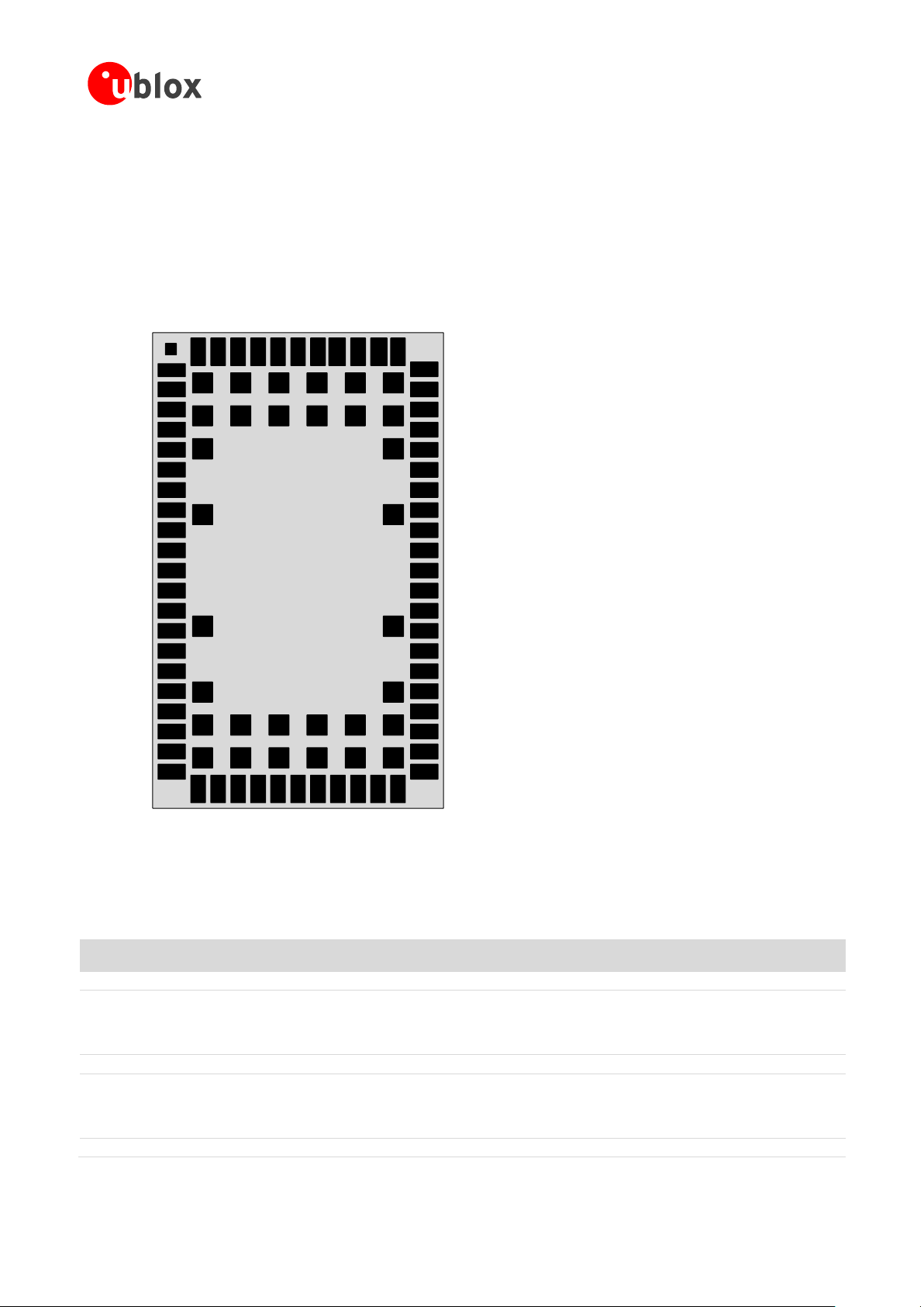
The SARA-U2 series modules are a 3.75G UMTS/HSPA solution with GSM/(E)GPRS fall-back in the miniature
(26.0 x 16.0 mm, 96-pin) SARA LGA form factor that allows seamless drop-in migration from / to other u-blox
cellular modules families.
SARA-U2 modules feature HSPA data-rates of 7.2 Mbit/s (downlink) and 5.76 Mbit/s (uplink). The modules offer
data and voice communication over an extended operating temperature range of –40 °C to +85 °C, with low
power consumption and a rich feature set including dual-stack IPv4 / IPv6.
The SARA-U2 series includes variants supporting band combinations for worldwide operation, for operation in
North America, Europe, Asia and other countries. A cost-saving UMTS-only variant is also available.
SARA-U2 modules are complete, fully qualified and certified solutions, which reduce costs and enable short time
to market. They are ideally suited to M2M applications such as: mobile internet terminals, car infotainment and
telematics, Automatic Meter Reading (AMR), Remote Monitoring Automation and Control (RMAC), surveillance
and security, road pricing, asset tracking, fleet management, anti-theft systems, and Point of Sales (PoS)
terminals. SARA-U2 modules support full access to u-blox GNSS receivers via serial port. Thus any host processor
connected to the cellular module through a single serial port can control both the cellular module and the
positioning chip/module. The compact SARA 26.0 x 16.0 mm form factor with LGA pads (functionally referred to
as “pins”) allows fully automated assembly with standard pick & place and reflow soldering equipment for costefficient, high-volume production.
1.2 Product features
Table 1: SARA-U2 series main features summary3
1
Second UART interface and FOTA not supported by "03" and "63" product versions
2
SARA-U270-73S and SARA-U270-53S module product versions do not support 2G radio access technology
3
SARA-U201 ATEX and SARA-U270 ATEX modules provide the same feature set as the SARA-U201 and SARA-U270 modules respectively,
with the additional certification for use in potentially explosive atmospheres. Unless otherwise specified, SARA-U201 refers to all
SARA-U201 ATEX and SARA-U201 modules; in the same way SARA-U270 refers to both SARA-U270 ATEX and SARA-U270 modules.
UBX-13005287 - R19 Functional description
Page 5 of 57
Page 6
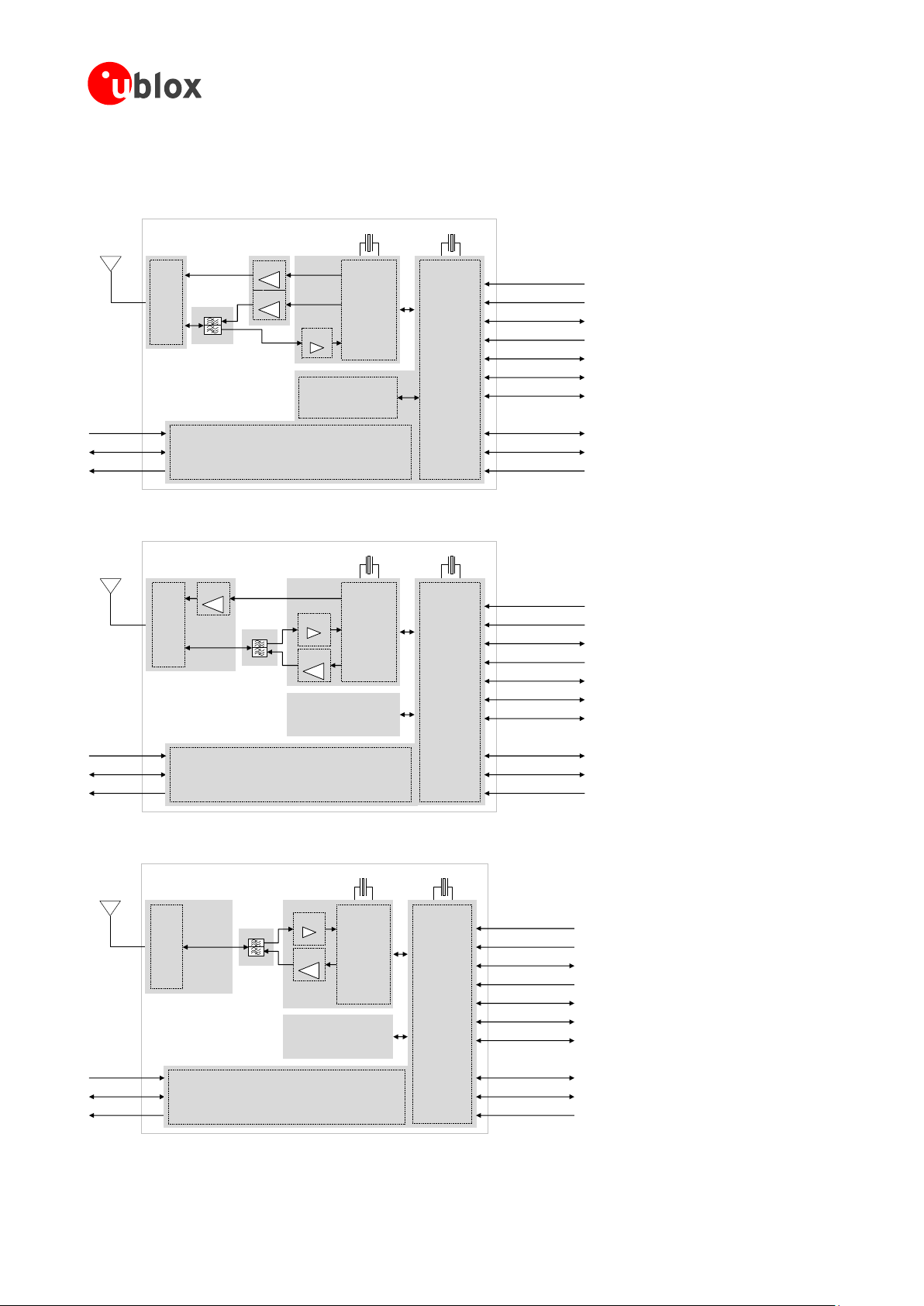
Memory
V_BCKP (RTC)
V_INT (I/O)
RF
transceiver
Power
Management
Cellular
BaseBand
Processor
ANT
VCC (Supply)
USB
DDC (I2C) / AUX UART
SIM card detection
SIM
UART
Power-On
Reset
Digital audio (I2S)
GPIO
Antenna detection
26 MHz
Duplexers
Filters
Switch
2G PA
32 kHz
LNAs
3G PA
Memory
V_BCKP (RTC)
V_INT (I/O)
RF
transceiver
Power
Management
Cellular
BaseBand
Processor
ANT
VCC (Supply)
USB
DDC (I2C)
SIM card detection
SIM
UART
Power-On
Reset
Digital audio (I2S)
GPIO
Antenna detection
3G PA
26 MHz
Duplexer
Filter
Switch
2G PA
LNA
32 kHz
Memory
V_BCKP (RTC)
V_INT (I/O)
RF
transceiver
Power
Management
Cellular
BaseBand
Processor
ANT
VCC (Supply)
USB
DDC (I2C)
SIM card detection
SIM
UART
Power-On
Reset
Digital audio (I2S)
GPIO
Antenna detection
3G PA
26 MHz
Duplexer
Filter
Switch
LNA
32 kHz
1.3 Block diagram
Figure 1: SARA-U201 block diagram
SARA-U2 series - Data Sheet
Figure 2: SARA-U260 and SARA-U270 block diagram
Figure 3: SARA-U280 block diagram
UBX-13005287 - R19 Functional description
Page 6 of 57
Page 7

SARA-U2 series - Data Sheet
3G UMTS/HSDPA/HSUPA characteristics
2G GSM/GPRS/EDGE characteristics4
Class A User Equipment5
Class B Mobile Station6
3GPP Release 7
High Speed Packet Access (HSPA)
UMTS Terrestrial Radio Access (UTRA)
Frequency Division Duplex (FDD)
3GPP Release 7
Enhanced Data rate GSM Evolution (EDGE)
GSM EGPRS Radio Access (GERA)
Time Division Multiple Access (TDMA)
Band support:
SARA-U201:
Band 19 (800 MHz)
Band 5 (850 MHz)
Band 8 (900 MHz)
Band 2 (1900 MHz)
Band 1 (2100 MHz)
Band support:
SARA-U201:
GSM 850 MHz
E-GSM 900 MHz
DCS 1800 MHz
PCS 1900 MHz
SARA-U260 and SARA-U280:
Band 5 (850 MHz)
Band 2 (1900 MHz)
SARA-U260:
GSM 850 MHz
PCS 1900 MHz
SARA-U270:
Band 8 (900 MHz)
Band 1 (2100 MHz)
SARA-U270:
E-GSM 900 MHz
DCS 1800 MHz
WCDMA/HSDPA/HSUPA Power Class
Power Class 3 (24 dBm) for WCDMA/HSDPA/HSUPA mode
GSM/GPRS Power Class
Power Class 4 (33 dBm) for GSM/E-GSM bands
Power Class 1 (30 dBm) for DCS/PCS bands
EDGE Power Class7
Power Class E2 (27 dBm) for GSM/E-GSM bands
Power Class E2 (26 dBm) for DCS/PCS bands
PS (Packet Switched) data rate
HSUPA category 6, up to 5.76 Mbit/s UL
HSDPA category 8, up to 7.2 Mbit/s DL
WCDMA PS data, up to 384 kbit/s DL/UL
PS (Packet Switched) data rate8
GPRS multi-slot class 12
9
, CS1-CS4 up to 85.6 kbit/s DL/UL
EDGE multi-slot class 12
10
, MCS1-MCS911 up to 236.8 kbit/s DL/UL
CS (Circuit Switched) data rate
WCDMA CS data, up to 64 kbit/s DL/UL
CS (Circuit Switched) data rate
GSM CS data, up to 9.6 kbit/s DL/UL
supported in transparent/non transparent mode
1.4 Product description
SARA-U2 series modules provide variants to support different band combinations for specific regions:
SARA-U201 modules are designed for worldwide operation
SARA-U260 and SARA-U280 modules are mainly designed for operation in America
SARA-U270 modules are mainly designed for operation in Europe, Asia and other countries
Table 2: SARA-U2 series 3G and 2G characteristics
4
Not supported by SARA-U270-73S, SARA-U270-53S and SARA-U280 modules
5
Device can work simultaneously in Packet Switch and Circuit Switch mode: voice calls are possible while the data connection is active
without any interruption in service.
6
Device can be attached to both GPRS and GSM services (i.e. Packet Switch and Circuit Switch mode) using one service at a time. If for
example during data transmission an incoming call occurs, the data connection is suspended to allow the voice communication. Once the
voice call has terminated, the data service is resumed.
7
SARA-U260 and SARA-U270 modules do not support 8-PSK modulation in uplink; the EDGE Power Class corresponds to the GSM/GPRS
Power Class
8
GPRS / EDGE multi-slot class determines the number of timeslots available for upload and download and thus the speed at which data can
be transmitted and received, with higher classes typically allowing faster data transfer rates.
9
GPRS multi-slot class 12 implies a maximum of 4 slots in DL (reception) and 4 slots in UL (transmission) with 5 slots in total.
10
EDGE multi-slot class 12 implies a maximum of 4 slots in DL (reception) and 4 slots in UL (transmission) with 5 slots in total.
11
SARA-U260, SARA-U270 modules support EDGE multi-slot class 12, MCS1-MCS9 up to 236.8 kbit/s DL, MCS1-MCS4 up to 70.4 kbit/s UL
UBX-13005287 - R19 Functional description
Page 7 of 57
Page 8

SARA-U2 series - Data Sheet
Basic features
Supplementary services
Short Message Service (SMS)
Display of Called Number
Call Hold/Resume (HOLD)
Text and PDU mode supported
Indication of Call Progress Signals
Call Waiting (CW)
Mobile-Originating SMS (MO SMS)
Country/PLMN Indication
Multi-Party (MTPY)
Mobile-Terminating SMS (MT SMS)
Country/PLMN Selection
Call Forwarding (CFU, CFB, CFNRy, CFNRc)
SMS indication and acknowledgement
International Access Function
Call Deflection (CD)
SMS Cell Broadcast (CBS)
Service Indicator
Explicit Call Transfer (ECT)
SMS during circuit-switched calls
Emergency Calls Capabilities
Call Barring (BAOC, BOIC, BOIC-exHC, BAIC, BIC_Roam)
SMS over CSD
Dual Tone Multi Frequency (DTMF)
Advice of Charge Charging (AoCC, AoCI)
SMS over PSD
Subscription Identity Management
Calling Line Identification Presentation (CLIP)
SMS storage on SIM
Service Provider Indication
Calling Line Identification Restriction (CLIR)
SMS storage on module memory
Abbreviated Dialing
Connected Line Identification Presentation (CoLP)
Concatenated SMS
Fixed Number Dialing
Connected Line Identification Restriction (CoLR)
Barring of Dialed Numbers
Unstructured Supplementary Services Data (USSD)
SIM Application Toolkit
Network Identify and Time Zone (NITZ)
ME-SIM lock
Calling Name Presentation (CNAP)
SIM Access Profile
Feature
Description
Network indication
GPIO configured to indicate the network status: registered home network, registered roaming, voice or data call
enabled, no service.
The feature can be enabled through the +UGPIOC AT command.
Antenna detection
The ANT_DET pin provides antenna presence detection capability, evaluating the resistance from the ANT pin to
GND by means of an external antenna detection circuit implemented on the application board.
The antenna detection feature can be enabled through the +UANTR AT command.
Operation modes I to III are supported on GSM/GPRS networks, with user-defined preferred service selectable
from GSM to GPRS. Paging messages for GSM calls can be optionally monitored during GPRS data transfer in
not-coordinating NOM II-III. Direct Link mode is supported for TCP and UDP sockets.
Table 3: SARA-U2 series mobile stations: basic features, supplementary services and SMS service summary12
1.5 AT command support
SARA-U2 series modules support AT commands according to the 3GPP Technical Specifications 27.007 [1],
27.005 [2], 27.010 [3], and the u-blox AT command extension.
For the complete list of supported AT commands and their syntax, see the u-blox AT Commands
Manual [4].
RIL (Radio Interface Layer) software for Android and Embedded Windows is available for SARA-U2 series
modules free of charge; see the Android RIL Production delivery [5] application note for more information.
1.6 Supported features
Table 4 lists the main features supported by SARA-U2 modules. For more details, see the SARA-G3 and SARA-U2
series System Integration Manual [6] and the u-blox AT commands manual [4].
12
All these functionalities are supported via AT commands (for more details see u-blox AT Commands Manual [4]).
UBX-13005287 - R19 Functional description
Page 8 of 57
Page 9
SARA-U2 series - Data Sheet
Feature
Description
Jamming detection
Detects some “artificial” interference that obscures the operator’s carriers entitled to give access to the
GSM/UMTS service and reports the start and stop of such conditions to the application processor (AP). The AP
can react appropriately by e.g. switching off the radio transceiver to reduce power consumption and monitoring
the environment at constant periods.
The feature can be enabled and configured through the +UCD AT command.
Embedded TCP and UDP
stack
Embedded TCP/IP and UDP/IP stack including direct link mode for TCP and UDP sockets.
Sockets can be set in Direct Link mode to establish a transparent end to end communication with an already
connected TCP or UDP socket via serial interface.
FTP, FTPS
File Transfer Protocol as well as Secure File Transfer Protocol (SSL encryption of FTP control channel)
functionalities are supported via AT commands.
HTTP, HTTPS
Hyper-Text Transfer Protocol as well as Secure Hyper-Text Transfer Protocol (SSL encryption) functionalities is
supported via AT commands. HEAD, GET, POST, DELETE and PUT operations are available. Up to four client
contexts can be simultaneously used.
Embedded TLS 1.214
With the support of X.509 certificates, Embedded TLS 1.2 provides server and client authentication, data
encryption, data signature and enables TCP/IP applications like HTTPS and FTPS to communicate over a secured
and trusted connection.
The feature can be configured and enabled by +USECMNG and +USECPRF AT commands.
IPv4/IPv6 dual-stack
Capability to move between IPv4 and dual stack network infrastructures using external context. IPv4 and IPv6
addresses can be used.
GNSS via modem
Full access to u-blox positioning chips and modules is available through a dedicated DDC (I2C) interface. This
means that from any host processor, a single serial port can control the cellular module and the positioning chip
or module. For more details, see the GNSS Implementation Application Note [7].
Embedded AssistNow
Software
Embedded AssistNow Online and AssistNow Offline clients to provide better GNSS performance and faster
Time-to-First-Fix. An AT command can enable / disable the clients.
CellLocate®
Enables the estimation of device position based on the parameters of the mobile network cells visible to the
specific device based on the CellLocate® database:
Normal scan: only the parameters of the visible home network cells are sent
Deep scan: the parameters of all surrounding cells of all mobile operators are sent
CellLocate® is implemented using a set of AT commands that allow configuration and position request.
Hybrid Positioning
The module current position is provided using a u-blox positioning chip or module or the estimated position from
CellLocate® depending by which positioning method provides the best and fastest solution according to the user
configuration.
Hybrid positioning is implemented through a set of AT commands that allow configuration and position request.
Control Plan Aiding /
LCS14
Assisted GPS Location Services feature, which is based on the Radio Resources Location Protocol (RRLP),
according to 3GPP TS 44.031 [9], and Radio Resource Control (RRC), according to 3GPP TS 25.331 [17]. With the
Assisted GPS feature, a location server provides the module with the GPS system information that otherwise
must be downloaded from satellites. The feature allows faster position fixes, increases sensitivity and reduces
module power consumption. The feature is invoked by the module through LCS Supplementary Services or by
the Network during emergency calls.
Firmware update Over
AT commands (FOAT)
Firmware module upgrade over UART and USB interface using AT command.
The firmware upgrade can be executed through the +UFWUPD AT command.
Smart Temperature
Supervisor
Constant monitoring of the module board temperature:
Warning notification when the temperature approaches an upper or lower predefined threshold
Shutdown notified and forced when the temperature value is outside the specified range (shutdown
suspended in case of an emergency call in progress)
The feature can be enabled or disabled through the +USTS AT command.
The sensor measures the board temperature, which can differ from the ambient temperature.
SIM Access Profile (SAP)
Allows access and use of a remote (U)SIM card instead of the local SIM card directly connected to the module
(U)SIM interface. The module acts as an SAP Client establishing a connection and performing data exchange to a
SAP Server directly connected to the remote SIM. The modules provide a dedicated USB SAP channel and a
dedicated multiplexer SAP channel over UART for communication with the remote (U)SIM card.
The feature can be configured and enabled by +USAPMODE and + USAPIND AT commands.
BIP
14
Bearer Independent Protocol for Over-the-Air SIM provisioning. The data transfer to/from the SIM uses either an
already active PDP context or a new PDP context established with the APN provided by the SIM card.
UBX-13005287 - R19 Functional description
Page 9 of 57
Page 10

SARA-U2 series - Data Sheet
Feature
Description
In-Band Modem13
In-Band modem solution for eCall and ERA-GLONASS emergency call applications over cellular networks
implemented according to the 3GPP TS 26.267 specification [8].
When activated, the in-vehicle eCall / ERA-GLONASS system (IVS) creates an emergency call carrying both voice
and data (including vehicle position data) directly to the nearest Public Safety Answering Point (PSAP) to
determine whether rescue services should be dispatched to the known position.
DTMF decoder
During a voice call, the Dual-Tone Multi-Frequency detector analyses the RX speech (coming from the remote
party). The detected DTMF symbols can be output via the related URC.
For more details, see the +UDTMFD AT command.
Power saving
The power saving configuration is disabled by default, but it can be configured using an AT command. When
power saving is enabled, the module automatically enters the low power idle-mode whenever possible, reducing
current consumption. During idle-mode, the module processor core runs with the RTC 32 kHz reference clock.
The feature can be enabled through the +UPSV AT command.
Automatic selection of
authentication type14
Automatic selection of authentication type during PDP context activation. The module will sequentially try
different authentication protocols (none/CHAP/PAP) until the authentication succeeds.
The feature can be enabled through the +UPSD and +UAUTHREQ AT commands.
Signal quality report for
Packet Switched calls14
The quality of the GPRS UL and/or DL connection is returned by the AT+CSQ command.
eMLPP14
Multi-Level Precedence and Pre-emption Service (eMLPP) permits to handle the call priority. The maximum
priority associated to a user is set in the SIM: within this threshold, the user can assign different priorities to the
calls. This results in a differentiated treatment of the calls by the network in case of abnormal events such as
handovers to congested cells.
The feature can be enabled through the +CAEMLPP, +CPPS, +CAAP AT commands.
Network Friendly Mode14
When the Network Friendly Mode is enabled, the module reacts to service request denials by using time-spaced,
randomized or delayed retry schemes according to GSMA IoT Device Connection Efficiency Guidelines [18].
The feature can be enabled through the +UNFM, +UNFMCONF and +URPM AT commands.
Ethernet (CDC-ECM)
over USB interface14
Ethernet (CDC-ECM) interface allowing networking from a HOST by means of the IP address received from the
cellular network (bridge mode).
The HOST configuration is performed via the DHCP protocol (a DHCP server is implemented).
It operates as a not exclusive alternative to PPP dial-up.
The feature can be configured by +UUSBCONF and enabled by +UCEDATA AT commands.
ODIS15
OMA-DM IMEI Sync (ODIS) is an AT&T functionality required at the cellular module level and used to identify the
end device operating inside the network.
Last gasp16
In case of power supply outage (i.e. main supply interruption, battery removal, battery voltage below a certain
threshold) the cellular module can be configured to send an alarm notification to a remote entity.
The feature can be enabled and configured through the +ULGASP AT command.
Firmware update Over
The Air (FOTA)16
Embedded FOTA client to enable the Firmware module update over the cellular air interface.
The feature can be enabled and configured through the +UFWINSTALL AT command.
Smart radio Coverage
Manager (SCM)16
Smart radio coverage manager is a feature that aims to reduce the power consumption in those cellular
scenarios where the radio coverage or the network conditions would cause an inefficient usage of power supply.
Table 4: Main supported features of the SARA-U2 series
u-blox is extremely mindful of user privacy. When a position is sent to the CellLocate
unable to track the SIM or the specific device that sent the position.
13
Not supported by SARA-U260 and SARA-U280 modules
14
Not supported by “00” product version
15
Not supported on SARA-U260, SARA-U270 and SARA-U280 modules
16
Not supported by "00","03","53","63","73" product versions
UBX-13005287 - R19 Functional description
Page 10 of 57
®
server, u-blox is
Page 11

SARA-U2 series - Data Sheet
2 Interfaces
2.1 Power management
2.1.1 Module supply (VCC)
SARA-U2 modules must be supplied through the VCC pins by a DC power supply. Voltages must be stable:
during operation, the current drawn from VCC can vary by some order of magnitude, especially due to the
surging consumption profile of the GSM system (described in the SARA-G3 and SARA-U2 series System
Integration Manual [6]). It is important that the system power supply circuit is able to support peak power.
2.1.2 RTC supply (V_BCKP)
V_BCKP is the Real Time Clock (RTC) supply of SARA-U2 modules. When VCC voltage is within the valid
operating range, the internal Power Management Unit (PMU) supplies the RTC and the same supply voltage is
available on V_BCKP pin. If the VCC voltage is under the minimum operating limit (e.g. during not powered
mode), the V_BCKP pin can externally supply the RTC.
2.1.3 Generic digital interfaces supply (V_INT)
SARA-U2 modules provide a 1.8 V supply rail output on the V_INT pin, which is internally generated when the
module is switched on. The same voltage domain is used internally to supply the generic digital interfaces of the
modules. The V_INT supply output can be used in place of an external discrete regulator optimizing the bill of
material for various applications, e.g. with u-blox GNSS receivers operating at 1.8 V.
2.2 Antenna
2.2.1 Antenna RF interface (ANT)
The ANT pin has an impedance of 50 and provides the RF antenna interface of SARA-U2 modules.
2.2.2 Antenna detection (ANT_DET)
The ANT_DET pin is an Analog to Digital Converter (ADC) input used to sense the antenna presence (as optional
feature), evaluating the resistance from the ANT pin to GND by means of an external antenna detection circuit
implemented on the application board (for more details, see the SARA-G3 and SARA-U2 series System
Integration Manual [6] and the u-blox AT Commands Manual [4], +UANTR).
2.3 System functions
2.3.1 Module power-on
SARA-U2 modules can be switched on in one of the following ways:
Rising edge on VCC pins to a valid voltage for module supply, i.e. applying module supply
Low pulse on PWR_ON pin, i.e. forcing the pin (normally high with external pull-up) to a low level for a valid
time period (see section 4.2.6): PWR_ON pin requires an external pull-up resistor to set its value to logic
high and may not be left floating
Rising edge on RESET_N pin, i.e. releasing the pin from the low level, normally high with internal pull-up
RTC alarm, i.e. pre-programmed scheduled time by AT+CALA command
UBX-13005287 - R19 Interfaces
Page 11 of 57
Page 12

SARA-U2 series - Data Sheet
2.3.2 Module power-off
SARA-U2 modules can be properly switched off, with storage of current parameter settings and network detach,
in one of these ways:
AT+CPWROFF command
Low pulse on the PWR_ON pin for at least 1 second
An abrupt under-voltage shutdown occurs on SARA-U2 modules when the VCC supply drops below the
extended operating range minimum limit, but in this case it is not possible to perform the storing of the current
parameter settings in the module’s non-volatile memory as well as the proper network detach.
An over-temperature or an under-temperature shutdown occurs on SARA-U2 modules when the temperature
measured within the cellular module reaches the dangerous area, if the optional Smart Temperature Supervisor
feature is enabled and configured by the dedicated AT command. For more details, see the SARA-G3 and
SARA-U2 series System Integration Manual [6] and the u-blox AT commands manual [4], +USTS AT command.
2.3.3 Module reset
SARA-U2 modules can be properly reset (rebooted), with storage of current parameter settings and network
detach, in this way:
By the AT+CFUN command (see the u-blox AT Commands Manual [4]). This causes an “internal” or
“software” reset of the baseband processor, excluding the integrated power management unit and the RTC
internal block: the V_INT generic digital interfaces supply is enabled and each digital pin is set to its internal
reset state (reported in Table 6), the V_BCKP supply and the RTC block are enabled.
An abrupt “external” or “hardware” reset occurs when a low level is applied to the RESET_N pin, which is
normally set high by an internal pull-up, for a valid time period (see section 4.2.7). This causes a reset of the
entire module, including the integrated power management unit, except for the RTC internal block: the V_INT
generic digital interfaces supply is switched off and all the digital pins are tri-stated, but the V_BCKP supply and
the RTC block are enabled. The current parameter settings are not saved in the module’s non-volatile memory
and a proper network detach is not performed.
2.4 SIM
2.4.1 (U)SIM interface
SARA-U2 modules provide a (U)SIM interface on the VSIM, SIM_IO, SIM_CLK, SIM_RST pins: the high-speed
SIM/ME interface is implemented as well as automatic detection of the required SIM supporting voltage.
Both 1.8 V and 3 V SIM card/chip types are supported (1.8 V and 3 V ME). Activation and deactivation with
automatic voltage switch from 1.8 V to 3 V is implemented, according to ISO-IEC 7816-3 specifications. The SIM
driver supports the PPS (Protocol and Parameter Selection) procedure for baud-rate selection, according to the
values proposed by the SIM card/chip.
2.4.2 SIM card detection (SIM_DET)
The SIM_DET pin of SARA-U2 modules is a 1.8 V digital input which is configured by default as an external
interrupt to detect the SIM card presence (as a feature which can be optionally used) when it is properly
connected to the mechanical switch of the SIM card holder (for more details, see the SARA-G3 and SARA-U2
series System Integration Manual [6]).
The SIM_DET pin of SARA-U2 modules can additionally be configured via AT command to provide the “SIM
card hot insertion/removal” function (for more details, see u-blox AT Commands Manual [4], +UDCONF=50).
The SIM_DET pin of SARA-U2 modules can additionally be configured via AT command as GPIO (for more
details, see section 2.7 and the u-blox AT Commands Manual [4], +UGPIOC, +UGPIOR, +UGPIOW).
UBX-13005287 - R19 Interfaces
Page 12 of 57
Page 13

SARA-U2 series - Data Sheet
2.5 Serial interfaces
SARA-U2 modules provide the following serial communication interfaces:
UART interface: 9-wire unbalanced 1.8 V asynchronous serial interface supporting (see 2.5.1)
o AT command mode
o Data mode and Online command mode
o MUX functionality, including dedicated GNSS tunneling and SIM Access Profile virtual channels
o FW upgrades by means of the FOAT feature
o FW upgrades by means of the u-blox EasyFlash tool
o Trace log capture (diagnostic purpose)
Auxiliary UART interface
function, in mutually exclusive way, over the DDC (I2C) interface’ pins, supporting (see 2.5.2)
o AT command mode
o Trace log capture (diagnostic purpose)
USB interface: High-Speed USB 2.0 compliant interface supporting (see 2.5.3)
o AT command mode
o Data mode and Online command mode
o GNSS tunneling and SIM Access Profile virtual channels
o Ethernet-over-USB
o FW upgrades by means of the FOAT feature
o FW upgrades by means of the u-blox EasyFlash tool
o Trace log capture (diagnostic purpose)
DDC interface: I
2
C-bus compatible 1.8 V interface supporting (see 2.5.4)
o Communication with u-blox GNSS positioning chips / modules
o Communication with other external I
17
17
18
: 3-wire unbalanced 1.8 V asynchronous serial interface, available as alternative
17
19
virtual channel
2
C devices as an audio codec
2.5.1 Asynchronous serial interface (UART)
The UART interface is a 9-wire 1.8 V unbalanced asynchronous serial interface supporting AT command mode,
Data mode and Online command mode, MUX functionality, including dedicated GNSS tunneling and SIM Access
Profile virtual channels, FW upgrades by means of the FOAT feature, FW upgrades by means of the u-blox
EasyFlash tool, and Trace log capture (diagnostic purpose).
The UART features are:
Complete serial port with RS-232 functionality conforming to the ITU-T V.24 Recommendation [10], with
CMOS compatible signal levels (0 V for low data bit or ON state and 1.8 V for high data bit or OFF state)
Data lines (RXD as output, TXD as input), hardware flow control lines (CTS as output, RTS as input), modem
status and control lines (DTR as input, DSR as output, DCD as output, RI as output) are provided
Hardware flow control (default value), software flow control, or none flow control are supported
Power saving indication available
OFF state when the module is not prepared to accept data by the UART interface
17
See the u-blox AT Commands Manual [4] for the definition of the command mode, data mode, and online command mode.
18
SARA-U2 modules product versions "00", "03", "53", "63", "73" do not provide Auxiliary UART interface.
19
SARA-U2 modules product versions "00" do not support Ethernet-over-USB.
20
If enabled
UBX-13005287 - R19 Interfaces
Page 13 of 57
20
on the hardware flow control output (CTS line): the line is driven to the
Page 14

SARA-U2 series - Data Sheet
1200, 2400, 4800, 9600, 19200, 38400, 57600, 115200, 230400, 460800 and 921600 bit/s baud rates are
supported for the AT interface
Autobauding is enabled by default
Frame format can be:
o 8N2 (8 data bits, no parity, 2 stop bits)
o 8N1 (8 data bits, no parity, 1 stop bit)
o 8E1 (8 data bits, even parity, 1 stop bit)
o 8O1 (8 data bits, odd parity, 1 stop bit)
o 7E1 (7 data bits, even parity, 1 stop bit)
o 7O1 (7 data bits, odd parity, 1 stop bit)
Default frame configuration is 8N1
The UART serial interface can be conveniently configured through AT commands. For more details, see the
u-blox AT Commands Manual [4] (+IPR, +ICF, +IFC, &K, \Q, +UPSV AT command) and the SARA-G3 and
SARA-U2 series System Integration Manual [6].
2.5.1.1 Autobauding feature
Only one shot autobauding is supported: the baud rate detection is performed only once, at module start-up.
After detection the module works at the fixed baud rate (the detected one) and the baud rate can only be
changed via the appropriate AT command (+IPR, for more details, see the u-blox AT Commands Manual [4]).
The module detects the followings baud rates (bit/s): 1200, 2400, 4800, 9600, 19200, 38400, 57600,
115200, 230400
The only detectable frame configurations are: 7E1, 7O1, 8N1, 8E1, 8O1
2.5.1.2 Multiplexer protocol
SARA-U2 module has a software layer with MUX functionality, 3GPP TS 27.010 Multiplexer Protocol [3],
available on the UART interface.
The multiplexer protocol is supported only over the UART physical interface.
This is a data link protocol (layer 2 of OSI model) which uses HDLC-like framing and operates between the
cellular module (Data Circuit-terminating Equipment) and the application processor (Data Terminal Equipment)
allowing simultaneous sessions over the UART physical link: the user can concurrently use the AT command
interface on one MUX channel and Data communication on another MUX channel. Each session consists of a
stream of bytes transferring various kinds of data such as SMS, CBS, PSD, GNSS, AT commands in general.
SARA-U2 modules provide the following virtual channels:
Channel 0: control channel
Channel 1 – 5: AT commands / data connection
Channel 6: GNSS tunneling
Channel 7: SAP (SIM Access Profile)
For more details, see the Mux Implementation Application Note [11].
UBX-13005287 - R19 Interfaces
Page 14 of 57
Page 15

SARA-U2 series - Data Sheet
2.5.2 Auxiliary asynchronous serial interface (AUX UART)
Not supported by "00", "03", "53", "63", "73" product versions.
The auxiliary UART interface is a 3-wire 1.8 V unbalanced asynchronous serial interface supporting AT command
mode and Trace log capture (diagnostic purpose).
The auxiliary UART interface is disabled by default, and it can be enabled by means of the +USIO AT command
(for more details, see the u-blox AT Commands Manual [4]), as alternative function of the DDC (I2C) interface’
pins, in mutually exclusive way with the DDC (I2C) interface.
The auxiliary UART features are:
Only the RXD_AUX data output and the TXD_AUX data input are provided, with CMOS compatible signal
levels (0 V for low data bit or ON state and 1.8 V for high data bit or OFF state)
Data lines (SCL pin configured as RXD_AUX output, SDA pin configured as TXD_AUX input)
Software flow control, or none flow control (default value) are supported
1200, 2400, 4800, 9600, 19200, 38400, 57600, 115200, 230400, 460800 and 921600 bit/s baud rates are
supported for the AT interface
Autobauding is enabled by default
Frame format can be:
o 8N2 (8 data bits, no parity, 2 stop bits)
o 8N1 (8 data bits, no parity, 1 stop bit)
o 8E1 (8 data bits, even parity, 1 stop bit)
o 8O1 (8 data bits, odd parity, 1 stop bit)
o 7E1 (7 data bits, even parity, 1 stop bit)
o 7O1 (7 data bits, odd parity, 1 stop bit)
Default frame configuration is 8N1
The auxiliary UART serial interface can be conveniently configured through AT commands. For more details, see
the u-blox AT Commands Manual [4] (+IPR, +ICF, +IFC, &K, \Q, +UPSV AT command) and the SARA-G3 and
SARA-U2 series System Integration Manual [6].
2.5.2.1 Autobauding feature
Only one shot autobauding is supported: the baud rate detection is performed only once, at module start-up.
After detection the module works at the fixed baud rate (the detected one) and the baud rate can only be
changed via the appropriate AT command (+IPR, for more details, see the u-blox AT Commands Manual [4]).
The module detects the followings baud rates (bit/s): 1200, 2400, 4800, 9600, 19200, 38400, 57600,
115200, 230400
The only detectable frame configurations are: 7E1, 7O1, 8N1, 8E1, 8O1
UBX-13005287 - R19 Interfaces
Page 15 of 57
Page 16

SARA-U2 series - Data Sheet
2.5.3 Universal Serial Bus (USB)
SARA-U2 series modules include a high-speed USB 2.0 compliant interface with a maximum 480 Mbit/s data
rate. The module itself acts as a USB device and can be connected to any USB host.
The USB is the suitable interface for transferring high speed data between SARA-U2 series and a host processor,
available for AT commands, data communication, FW upgrade by means of the FOAT feature, FW upgrade by
means of the u-blox EasyFlash tool and for diagnostic purpose.
The USB_D+ / USB_D- lines carry the USB serial data and signaling. The USB interface is automatically enabled
by an external valid USB VBUS supply voltage (5.0 V typical) applied on the VUSB_DET pin.
SARA-U2 series modules can provide the following functions over the USB interface:
CDC-ACM for AT commands and data communication
CDC-ACM for GNSS tunneling
CDC-ACM for diagnostic
CDC-ACM for SAP (SIM Access Profile)
CDC-ECM for Ethernet-over-USB
CDC-ECM for Ethernet-over-USB function is not supported by the “00” product version.
The default configuration of the USB interface provides 7 USB CDC-ACM modem COM ports:
USB1: AT and data
USB2: AT and data
USB3: AT and data
USB4: GNSS tunneling
USB5: Primary Log (diagnostic purpose)
USB6: Secondary Log (diagnostic purpose)
USB7: SAP (SIM Access Profile)
The user can concurrently use the AT command interface on one CDC, and Packet-Switched / Circuit-Switched
Data communication on another CDC.
The USB interface can be configured by the AT+UUSBCONF command to provide a different set of functions,
including 1 CDC-ECM for Ethernet-over-USB and 4 CDC-ACM modem COM ports enumerated as follows:
USB1: AT and data
USB2: GNSS tunneling
USB3: Primary Log (diagnostic purpose)
USB4: SAP (SIM Access Profile)
The default profile of the USB interface cannot be changed on the “00” product version.
For more details regarding the USB configurations and capabilities, see the SARA-G3 and SARA-U2 series System
Integration Manual [6] and the u-blox AT Commands Manual [4] (+UUSBCONF AT command).
UBX-13005287 - R19 Interfaces
Page 16 of 57
Page 17

SARA-U2 series - Data Sheet
USB drivers are available for the following operating system platforms:
Windows XP
Windows Vista
Windows 7
Windows 8
Windows 8.1
Windows 10
Windows CE 5.0
Windows Embedded CE 6.0
Windows Embedded Compact 7
Windows Embedded Automotive 7
Windows Mobile 5
Windows Mobile 6
Windows Mobile 6.1
Windows Mobile 6.5
SARA-U2 modules are compatible with the standard Linux/Android USB kernel drivers.
2.5.4 DDC (I
2
C) bus interface
SARA-U2 modules include an I2C compatible DDC interface (SDA, SCL) available to communicate with a u-blox
GNSS receiver and with external I2C devices as an audio codec: SARA-U2 module acts as an I2C master which can
communicate with I2C slaves in accordance to the I2C bus specifications [12].
2.6 Audio
SARA-U2 modules have one 4-wire I2S digital audio interface (I2S_CLK, I2S_RXD, I2S_TXD and I2S_WA) that
can be configured by AT commands in PCM or in normal I2S mode. (For more details, see the u-blox AT
Commands Manual [4] and the SARA-G3 and SARA-U2 series System Integration Manual [6].)
SARA-U2 modules provide a digital clock output (CODEC_CLK) for an external audio codec.
UBX-13005287 - R19 Interfaces
Page 17 of 57
Page 18
SARA-U2 series - Data Sheet
Function
Description
Module
Default GPIO
Configurable GPIOs
GSM Tx-burst
indication
GSM transmit slot indication
SARA-U201,
SARA-U260,
SARA-U270
--
GPIO1
GNSS supply enable
Enable/disable the supply of the u-blox GNSS
receiver connected to the cellular module
All
GPIO2
GPIO1, GPIO2,
GPIO3, GPIO4,
SIM_DET
GNSS data ready
Input to sense when the u-blox GNSS receiver
connected to the cellular module is ready for
sending data over the DDC (I2C) interface
All
GPIO3
GPIO3
GNSS RTC sharing
RTC synchronization signal to the u-blox GNSS
receiver connected to the cellular module
All
GPIO4
GPIO4
SIM card detection
SIM card physical presence detection
All
SIM_DET
SIM_DET
SIM card hot insertion
Enable/disable SIM interface upon detection of
external SIM card physical insertion/removal
All
--
SIM_DET
Last gasp21
Input to trigger the delivery of a last alarm
notification to a remote entity
SARA-U201
--
GPIO3
Network status
indication
Network status: registered 2G / 3G home
network, registered 2G / 3G roaming, 2G / 3G
data transmission, no service
All
--
GPIO1, GPIO2,
GPIO3, GPIO4,
SIM_DET
Module status
indication
Module status: power off mode, i.e. module
switched off, versus idle, active or connected
mode, i.e. module switched on
All
--
GPIO1
Module operating
mode indication
Module operating mode: idle mode versus
active or connected mode
All
--
SIM_DET
I2S digital audio
interface
I2S digital audio interface (I2S_RXD, I2S_TXD,
I2S_CLK, I2S_WA respectively)
All
I2S_RXD, I2S_TXD,
I2S_CLK, I2S_WA
I2S_RXD, I2S_TXD,
I2S_CLK, I2S_WA
General purpose input
Input to sense high or low digital level
All
--
All
General purpose
output
Output to set the high or the low digital level
All
--
All
Pin disabled
Tri-state with an internal active pull-down
enabled
All
GPIO1
All
2.7 GPIO
SARA-U2 modules provide nine pins (GPIO1, GPIO2, GPIO3, GPIO4, I2S_RXD, I2S_TXD, I2S_CLK, I2S_WA,
SIM_DET) which can be configured as general purpose input/output, or to provide the custom functions listed in
Table 5 via u-blox AT commands. For further details, see the SARA-G3 and SARA-U2 series System Integration
Manual [6] and the u-blox AT Commands Manual [4], +UGPIOC, +UGPIOR, +UGPIOW, +UGPS, +UGPRF,
+USPM, +UDCONF=50, +ULGASP AT commands.
Table 5: GPIO custom functions configuration
21
Not supported by "03", "63" product versions
UBX-13005287 - R19 Interfaces
Page 18 of 57
Page 19
64 63 61 60 58 57 55 54
22 23 25 26 28 29 31 32
11
10
8
7
5
4
2
1
21
19
18
16
15
13
12
43
44
46
47
49
50
52
53
33
35
36
38
39
41
42
65 66 67 68 69 70
71 72 73 74 75 76
77 78
79 80
81 82
83 84
85 86 87 88 89 90
91 92 93 94 95 96
CTS
RTS
DCD
RI
V_INT
V_BCKP
GND
CODEC_CLK
RESET_N
GPIO1
PWR_ON
RXD
TXD
3
20
17
14
9
6
24 27 30
51
48
45
40
37
34
5962 56
GND
GND
DSR
DTR
GND
VUSB_DET
GND
GND
USB_D-
USB_D+
RSVD
GND
GPIO2
GPIO3
SDA
SCL
GPIO4
GND
GND
GND
RSVD
RSVD
RSVD
RSVD
GND
VCC
VCC
RSVD
I2S_TXD
I2S_CLK
SIM_CLK
SIM_IO
VSIM
SIM_DET
VCC
RSVD
RSVD
SIM_RST
I2S_RXD
I2S_WA
GND
GND
GND
GND
GND
GND
GND
GND
GND
ANT_DET
ANT
SARA-U2
Top View
Pin 65-96: GND
No
Name
Power
domain
I/O
Description
Remarks
1
GND - N/A
Ground
All the GND pins must be connected to ground
2
V_BCKP
-
I/O
Real Time Clock supply
input/output
V_BCKP = 1.8 V (typical) generated by the module to supply the
Real Time Clock when VCC supply voltage is within valid
operating range.
See section 4.2.2 for detailed electrical specs.
3
GND - N/A
Ground
All the GND pins must be connected to ground
4
V_INT
-
O
Generic Digital Interfaces
supply output
V_INT = 1.8 V (typical) generated by the module when it is
switched on and the RESET_N (external reset input pin) is not
forced to the low level.
See section 4.2.2 for detailed electrical specs.
5
GND - N/A
Ground
All the GND pins must be connected to ground
3 Pin definition
3.1 Pin assignment
SARA-U2 series - Data Sheet
Figure 4: SARA-U2 series pin assignment
UBX-13005287 - R19 Pin definition
Page 19 of 57
Page 20

SARA-U2 series - Data Sheet
No
Name
Power
domain
I/O
Description
Remarks
6
DSR
GDI O UART data set ready
Circuit 107 (DSR) in ITU-T V.24.
Output driver class D.
PU/PD class a. Value at internal reset: T/PU.
See section 4.2.9 for detailed electrical specs.
7
RI
GDI O UART ring indicator
Circuit 125 (RI) in ITU-T V.24.
Output driver class C_0.
PU/PD class c. Value at internal reset: T/PD.
See section 4.2.9 for detailed electrical specs.
8
DCD
GDI O UART data carrier detect
Circuit 109 (DCD) in ITU-T V.24.
Output driver class C_0.
PU/PD class c. Value at internal reset: T/PD.
See section 4.2.9 for detailed electrical specs.
9
DTR
GDI
I
UART data terminal
ready
Circuit 108/2 (DTR) in ITU-T V. 24.
Internal active pull-up to V_INT enabled.
PU/PD class c. Value at internal reset: T/PD.
See section 4.2.9 for detailed electrical specs.
10
RTS
GDI I UART ready to send
Circuit 105 (RTS) in ITU-T V.24.
Internal active pull-up to V_INT enabled.
PU/PD class a. Value at internal reset: T/PU.
See section 4.2.9 for detailed electrical specs.
11
CTS
GDI O UART clear to send
Circuit 106 (CTS) in ITU-T V.24.
Output driver class A.
PU/PD class a. Value at internal reset: T/PU.
See section 4.2.9 for detailed electrical specs.
12
TXD
GDI I UART data input
Circuit 103 (TxD) in ITU-T V.24.
Internal active pull-up to V_INT enabled.
PU/PD class a. Value at internal reset: T/PD.
See section 4.2.9 for detailed electrical specs.
13
RXD
GDI O UART data output
Circuit 104 (RxD) in ITU-T V.24.
Output driver class A.
PU/PD class a. Value at internal reset: T/PU.
See section 4.2.9 for detailed electrical specs.
14
GND - N/A
Ground
All the GND pins must be connected to ground
15
PWR_ON
POS I Power-on input
The PWR_ON pin has high input impedance:
don’t leave it floating in noisy environment
(an external pull-up resistor is required)
See section 4.2.6 for detailed electrical specs.
16
GPIO1
GDI
I/O
GPIO
GPIO configurable as described in Table 5.
Output driver class A.
PU/PD class a. Value at internal reset: T/PD.
See section 4.2.9 for detailed electrical specs.
17
VUSB_DET
USB I USB detect input
Input for VBUS (5 V typical) USB supply sense.
See section 4.2.10 for detailed electrical specs.
18
RESET_N
ERS I External reset input
Internal 10 k pull-up resistor to V_BCKP.
See section 4.2.7 for detailed electrical specs.
19
CODEC_CLK
GDI O Clock output
Output driver class B.
PU/PD class b. Value at internal reset: T/PD.
See section 4.2.9 for detailed electrical specs.
20
GND - N/A
Ground
All the GND pins must be connected to ground
21
GND - N/A
Ground
All the GND pins must be connected to ground
22
GND - N/A
Ground
All the GND pins must be connected to ground
23
GPIO2
GDI
I/O
GPIO
GPIO configurable as described in Table 5.
Output driver class A.
PU/PD class a. Value at internal reset: T/PD.
See section 4.2.9 for detailed electrical specs.
UBX-13005287 - R19 Pin definition
Page 20 of 57
Page 21

SARA-U2 series - Data Sheet
No
Name
Power
domain
I/O
Description
Remarks
24
GPIO3
GDI
I/O
GPIO
GPIO configurable as described in Table 5.
Output driver class A.
PU/PD class a. Value at internal reset: T/PD.
See section 4.2.9 for detailed electrical specs.
25
GPIO4
GDI
I/O
GPIO
GPIO configurable as described in Table 5.
Output driver class A.
PU/PD class a. Value at internal reset: T/PD.
See section 4.2.9 for detailed electrical specs.
26
SDA
DDC
I/O
I2C bus data line
Fixed open drain. No internal pull-up.
Value at internal reset: T.
See section 4.2.11 for detailed electrical specs.
GDI I AUX UART data input
Not supported by "00","03","53","63","73" product versions
Circuit 103 (TxD) in ITU-T V.24.
Internal active pull-up to V_INT enabled.
PU/PD class a. Value at internal reset: T.
See section 4.2.9 for detailed electrical specs.
27
SCL
DDC O I2C bus clock line
Fixed open drain. No internal pull-up.
Value at internal reset: T.
See section 4.2.11 for detailed electrical specs.
GDI O AUX UART data output
Not supported by "00","03","53","63","73" product versions
Circuit 104 (RxD) in ITU-T V.24.
Output driver class E.
PU/PD class a. Value at internal reset: T.
See section 4.2.9 for detailed electrical specs.
28
USB_D-
USB
I/O
USB Data Line D-
90 nominal differential impedance.
Pull-up, pull-down and series resistors as required by USB 2.0
specifications [15] are part of the USB pin driver and need not
be provided externally.
Value at internal reset: T.
See section 4.2.10 for detailed electrical specs.
29
USB_D+
USB
I/O
USB Data Line D+
90 nominal differential impedance.
Pull-up, pull-down and series resistors as required by USB 2.0
specifications [15] are part of the USB pin driver and need not
be provided externally.
Value at internal reset: T.
See section 4.2.10 for detailed electrical specs.
30
GND - N/A
Ground
All the GND pins must be connected to ground
31
RSVD
-
N/A
RESERVED pin
Leave unconnected.
32
GND - N/A
Ground
All the GND pins must be connected to ground
33
RSVD
-
N/A
RESERVED pin
This pin must be connected to GND.
34
I2S_WA
GDI
I/O /
I/O
I2S word alignment /
GPIO
Configurable as I2S word alignment (Input with internal active
pull-down enabled in slave mode, Output in master mode), or
as GPIO (see Table 5).
Output driver class C.
PU/PD class a. Value at internal reset: T/PD.
See section 4.2.9 for detailed electrical specs.
35
I2S_TXD
GDI
O /
I/O
I2S transmit data /
GPIO
Configurable as I2S transmit data out, or as GPIO (see Table 5)
Output driver class C.
PU/PD class a. Value at internal reset: T/PD.
See section 4.2.9 for detailed electrical specs.
36
I2S_CLK
GDI
I/O /
I/O
I2S clock /
GPIO
Configurable as I2S clock (Input with internal active pull-down in
slave mode, Output in master mode), or as GPIO (see Table 5).
Output driver class C.
PU/PD class a. Value at internal reset: T/PD.
See section 4.2.9 for detailed electrical specs.
UBX-13005287 - R19 Pin definition
Page 21 of 57
Page 22
SARA-U2 series - Data Sheet
No
Name
Power
domain
I/O
Description
Remarks
37
I2S_RXD
GDI
I /
I/O
I2S receive data /
GPIO
Configurable as I2S receive data input (with internal active pulldown enabled), or as GPIO (see Table 5).
Output driver class C.
PU/PD class a. Value at internal reset: T/PD.
See section 4.2.9 for detailed electrical specs.
38
SIM_CLK
SIM O SIM clock
Value at internal reset: L.
See section 4.2.8 for detailed electrical specs.
39
SIM_IO
SIM
I/O
SIM data
Internal 4.7 k pull-up resistor to VSIM.
Value at internal reset: L/PD.
See section 4.2.8 for detailed electrical specs.
40
SIM_RST
SIM O SIM reset
Value at internal reset: L.
See section 4.2.8 for detailed electrical specs.
41
VSIM - O
SIM supply output
VSIM = 1.80 V typical or 2.90 V typical generated by the
module according to the SIM card type.
See section 4.2.2 for detailed electrical specs.
42
SIM_DET
GDI
I
SIM detection
Configurable for the SIM card presence detection function, or
as GPIO (see Table 5).
PU/PD class a. Value at internal reset: T/PD.
See section 4.2.9 for detailed electrical specs.
43
GND - N/A
Ground
All the GND pins must be connected to ground
44
RSVD
-
N/A
RESERVED pin
Leave unconnected.
45
RSVD
-
N/A
RESERVED pin
Leave unconnected.
46
RSVD
-
N/A
RESERVED pin
Leave unconnected.
47
RSVD
-
N/A
RESERVED pin
Leave unconnected.
48
RSVD
-
N/A
RESERVED pin
Leave unconnected.
49
RSVD
-
N/A
RESERVED pin
Leave unconnected.
50
GND - N/A
Ground
All the GND pins must be connected to ground
51
VCC - I
Module supply input
All VCC pins must be connected to external supply.
See sections 4.2.2 and 4.2.3 for detailed specs.
52
VCC - I
Module supply input
All VCC pins must be connected to external supply.
See sections 4.2.2 and 4.2.3 for detailed specs.
53
VCC - I
Module supply input
All VCC pins must be connected to external supply.
See sections 4.2.2 and 4.2.3 for detailed specs.
54
GND - N/A
Ground
All the GND pins must be connected to ground
55
GND - N/A
Ground
All the GND pins must be connected to ground
56
ANT - I/O
RF input/output
50 nominal impedance
See section 4.2.4 for detailed electrical specs.
57
GND - N/A
Ground
All the GND pins must be connected to ground
58
GND - N/A
Ground
All the GND pins must be connected to ground
59
GND - N/A
Ground
All the GND pins must be connected to ground
60
GND - N/A
Ground
All the GND pins must be connected to ground
61
GND - N/A
Ground
All the GND pins must be connected to ground
62
ANT_DET
ADC
I
Antenna detection
Antenna presence detection function.
See section 4.2.5 for detailed electrical specs.
63
GND - N/A
Ground
All the GND pins must be connected to ground
64
GND - N/A
Ground
All the GND pins must be connected to ground
65-96
GND - N/A
Ground
All the GND pins must be connected to ground
Table 6: SARA-U2 series module pin-out
For more information about pin-outs, see the SARA-G3 and SARA-U2 series System Integration
Manual [6].
For an explanation of the abbreviations and terms used, see Appendix A.
UBX-13005287 - R19 Pin definition
Page 22 of 57
Page 23
SARA-U2 series - Data Sheet
Symbol
Description
Condition
Min.
Max.
Unit
VCC
Module supply voltage
Input DC voltage at VCC pins
-0.30
5.50 V VUSB_DET
USB detection pin
Input DC voltage at VUSB_DET pin
-0.30
5.35
V
USB
USB D+/D- pins
Input DC voltage at USB_D+ and USB_D- pins
-1.00
5.35
V
V_BCKP
RTC supply voltage
Input DC voltage at V_BCKP pin
-0.15
2.00
V
GDI
Generic digital interfaces
Input DC voltage at Generic digital interfaces pins
-0.30
3.60 V DDC
DDC interface
Input DC voltage at DDC interface pins
-0.30
3.60 V SIM
SIM interface
Input DC voltage at SIM interface pin
-0.30
3.60 V ERS
External reset signal
Input DC voltage at RESET_N external reset pin
-0.15
2.10 V POS
Power-on signal
Input DC voltage at PWR_ON power-on pin
-0.30
5.50
V
ADC
Antenna detection pin
Input DC voltage at ANT_DET pin
-0.15
3.00 V P_ANT
Antenna power
Input in-band RF power at ANT pin
-10
dBm
Rho_ANT
Antenna ruggedness
Output RF load mismatch ruggedness at ANT pin
15:1
VSWR
Tstg
Storage temperature
-40
90
°C
Parameter
Module
Max.
Unit
Remarks
ESD sensitivity for all pins except ANT pin
All
1000
V
Human Body Model according to JESD22-A114F
ESD sensitivity for ANT pin
All
1000
V
Human Body Model according to JESD22-A114F
ESD immunity for ANT pin
SARA-U201
4000
V
Contact Discharge according to IEC 61000-4-2
8000
V
Air Discharge according to IEC 61000-4-2
All except SARA-U201
2000
V
Contact Discharge according to IEC 61000-4-2
4000
V
Air Discharge according to IEC 61000-4-2
4 Electrical specifications
Stressing the device above one or more of the ratings listed in the Absolute Maximum Rating
section may cause permanent damage. These are stress ratings only. Operating the module at
these or at any conditions other than those specified in the Operating Conditions sections
(section 4.2) of the specification should be avoided. Exposure to Absolute Maximum Rating
conditions for extended periods may affect device reliability.
Operating conditions ranges define those limits within which the functionality of the device is guaranteed.
Electrical characteristics are defined according to verification on a representative number of samples or
according to simulation.
Where application information is given, it is advisory only and does not form part of the specification.
4.1 Absolute maximum rating
Limiting values given below are in accordance with the Absolute Maximum Rating System (IEC 134).
Table 7: Absolute maximum ratings
The product is not protected against overvoltage or reversed voltages. If necessary, voltage
spikes exceeding the power supply voltage specification, given in the table above, must be
limited to values within the specified boundaries by using appropriate protection devices.
4.1.1 Maximum ESD
Table 8: Maximum ESD ratings
SARA-U2 modules are Electrostatic Sensitive Devices (ESD) and require special precautions when
handling. See section 7.4 for ESD handling instructions.
UBX-13005287 - R19 Electrical specifications
Page 23 of 57
Page 24
SARA-U2 series - Data Sheet
Symbol
Parameter
Module
Min.
Typ.
Max.
Units
Remarks
Topr
Operating
temperature range
All
-40 +85
°C
Normal operating
temperature range
SARA-U201
-20 +65
°C
See section 4.2.1.1
SARA-U260,
SARA-U270,
SARA-U280
-20 +55
°C
See section 4.2.1.1
Extended operating
temperature range
All
-40 -20
°C
Extended operating
temperature range 1
See section 4.2.1.2
SARA-U201
+65 +85
°C
Extended operating
temperature range 2
See section 4.2.1.3
SARA-U260,
SARA-U270,
SARA-U280
+55 +85
°C
Extended operating
temperature range 2
See section 4.2.1.3
4.2 Operating conditions
Unless otherwise indicated, all operating condition specifications assume an ambient temperature of
+25 °C.
Operation beyond the operating conditions is not recommended and extended exposure
beyond them may affect device reliability.
4.2.1 Operating temperature range
Table 9: Environmental conditions
4.2.1.1 Normal operating temperature range
The cellular module is fully functional and meets the 3GPP specification across the specified temperature range.
4.2.1.2 Extended operating temperature range 1
The cellular module is fully functional across the specified temperature range. Occasional deviations from the
3GPP specification may occur.
4.2.1.3 Extended operating temperature range 2
The cellular module is functional across the specified temperature range. Occasional deviations from the 3GPP
specification may occur. Thermal protection including automatic shutdown is implemented for protection against
overheating. Thermal protection is disabled for emergency calls. For more details, see the u-blox AT Commands
Manual [4], +USTS AT command).
UBX-13005287 - R19 Electrical specifications
Page 24 of 57
Page 25
Symbol
Parameter
Min.
Typ.
Max.
Unit
VCC
Module supply normal operating input voltage22
3.30
3.80
4.40 V
Module supply extended operating input voltage23
3.10 4.50 V V_BCKP
RTC supply input voltage
1.00
1.80
1.90
V
I_BCKP
RTC supply average current consumption,
at V_BCKP = 1.8 V
2.00 µA
Symbol
Parameter
Min.
Typ.
Max.
Unit
VSIM
SIM supply output voltage
1.76
1.80
1.83 V 2.84
2.90
2.94 V V_BCKP
RTC supply output voltage
1.71
1.80
1.89 V I_BCKP
RTC supply output current capability
3
mA
V_INT
Digital I/O Interfaces supply output voltage
1.73
1.80
1.87
V
V_INT_RIPPLE
Digital I/O Interfaces supply output peak-to-peak
voltage ripple during active or connected mode
15
mV
Digital I/O Interfaces supply output peak-to-peak
voltage ripple during low power idle mode with power
saving enabled by AT+UPSV command
70
mV
I_INT
Digital I/O Interfaces supply output current capability
70
mA
4.2.2 Supply/Power pins
Table 10: Input characteristics of the Supply/Power pins
SARA-U2 series - Data Sheet
Table 11: Output characteristics of the Supply/Power pins
22
Input voltage at VCC must be above the normal operating range minimum limit to switch on the module.
23
Occasional deviations from the 3GPP specifications may occur. Ensure that input voltage at VCC never drops below the extended operating
range minimum limit during module operation: the module may switch off when the VCC voltage value drops below the extended operating
range minimum limit.
UBX-13005287 - R19 Electrical specifications
Page 25 of 57
Page 26

Mode
Condition
Band
Module
Min
Typ24
Max25
Unit
Power Off Mode
Averaged current, module switched off
SARA-U201
55 µA
SARA-U260,
SARA-U270,
SARA-U280
65 µA
Idle-Mode
(Power Saving enabled by
AT+UPSV, module in low
power idle-mode, equivalent
to +CFUN=0)
Averaged current over a 100 ms period,
USB interface disconnected
All 0.5 mA
Averaged current over a 100 ms period,
USB interface connected and suspended
All 0.9 mA
2G Cyclic Idle/Active-Mode
(Power Saving enabled by
AT+UPSV, Module registered
with network)
Averaged current over a 10 minute period,
DRX = 926, +UPSV=2 or 3, USB disconnected
All
All 0.9 mA
Averaged current over a 10 minute period,
DRX = 527, +UPSV=1, USB disconnected
All
All 1.2 mA
Averaged current over a 10 minute period,
DRX = 527, +UPSV=1, USB suspended
All
All 1.6 mA
2G Active-Mode
(Power Saving disabled by
AT+UPSV=0, Module
registered with network)
Averaged current over a 10 minute period,
DRX = 527, USB disconnected
All
All 14.7 mA
Averaged current over a 10 minute period,
DRX = 527, USB connected and not
suspended
All
All 34.3 mA
GSM Connected Mode
(Tx / Rx call enabled)
Peak current28 during a 1-slot Tx burst
Maximum Tx power
850, 900
All 1.55
1.90
A
Averaged current over a 10 second period,
1 Tx + 1 Rx slot, Minimum Tx power
All
SARA-U201,
SARA-U260,
SARA-U270
45 mA
Averaged current over a 10 second period,
1 Tx + 1 Rx slot, Maximum Tx power
850, 900
SARA-U201
240 mA
SARA-U260,
SARA-U270
210 mA
1800, 1900
SARA-U201
160 mA
SARA-U260,
SARA-U270
135 mA
GPRS Connected Mode
(Tx / Rx call enabled)
Averaged current over a 10 second period,
4 Tx + 1 Rx slots, Maximum Tx power29
850, 900
SARA-U201
600 mA
SARA-U260,
SARA-U270
560 mA
1800, 1900
SARA-U201
400 mA
SARA-U260,
SARA-U270
350 mA
EDGE Connected Mode
(Tx / Rx call enabled)
Averaged current over a 10 second period,
4 Tx + 1 Rx slots, Maximum Tx power29
850, 900
SARA-U201
470 mA
1800, 1900
SARA-U201
490 mA
4.2.3 Current consumption
SARA-U2 series - Data Sheet
24
Typical values with a matched antenna
25
Maximum values with a mismatched antenna
26
Module is registered with the network, with a paging period of 2.12 s (2G network DRX setting = 9), with none neighbour cell.
27
Module is registered with the network, with a paging period of 1.18 s (2G network DRX setting = 5), with 16 neighbour cells.
28
It is recommended to use this figure to dimension maximum current capability of power supply.
29
Condition for GPRS and EDGE multi-slot output power: Multi-Slot Power Reduction profile 2 (+UDCONF=40 AT command default value).
UBX-13005287 - R19 Electrical specifications
Page 26 of 57
Page 27

SARA-U2 series - Data Sheet
Mode
Condition
Band
Module
Min
Typ24
Max25
Unit
3G Cyclic Idle/Active-Mode
(Power Saving enabled by
AT+UPSV, Module registered
with network)
Averaged current over a 10 minute period,
DRX = 930, +UPSV=2 or 3, USB disconnected
All
All 0.9 mA
Averaged current over a 10 minute period,
DRX = 731, +UPSV=1, USB disconnected
All
All 1.3 mA
Averaged current over a 10 minute period,
DRX = 731, +UPSV=1, USB suspended
All
All 1.7 mA
3G Active-Mode
(Power Saving disabled by
AT+UPSV=0, Module
registered with network)
Averaged current over a 10 minute period,
DRX = 731, USB disconnected
All
All 14.1 mA
Averaged current over a 10 minute period,
DRX = 731, USB connected and not suspended
All
All 33.7 mA
UMTS Connected Mode
(Tx / Rx call enabled)
Averaged current over a 10 second period,
12.2 kbit/s UL, 12.2 kbit/s DL
Minimum Tx power
1, 2
All 120 mA
5, 8, 19
All 115 mA
Averaged current over a 10 second period,
12.2 kbit/s UL, 12.2 kbit/s DL
Tx power = 0 dBm
1, 2
All 140 mA
5, 8, 19
All 135 mA
Averaged current over a 10 second period,
12.2 kbit/s UL, 12.2 kbit/s DL
Tx power = 12 dBm
1, 2
All 200 mA
5, 8, 19
All 190 mA
Averaged current over a 10 second period,
12.2 kbit/s UL, 12.2 kbit/s DL
Tx power = 18 dBm
1, 2
All 350 mA
5, 8, 19
All 325 mA
Averaged current over a 10 second period,
12.2 kbit/s UL, 12.2 kbit/s DL
Maximum Tx power
1, 2
SARA-U201
510 mA
SARA-U260,
SARA-U270,
SARA-U280
625 mA
5, 8, 19
SARA-U201
430 mA
SARA-U260,
SARA-U270,
SARA-U280
565 mA
HSDPA Connected Mode
(Tx / Rx call enabled)
Averaged current over a 10 second period,
Maximum DL data rate (HSDPA)
Maximum Tx power
1, 2
SARA-U201
550 mA
SARA-U260,
SARA-U270,
SARA-U280
680 mA
5, 8, 19
SARA-U201
500 mA
SARA-U260,
SARA-U270,
SARA-U280
595 mA
HSUPA or HSPA
Connected Mode
(Tx / Rx call enabled)
Averaged current over a 10 second period,
Maximum UL data rate (HSUPA) or
Maximum both UL/DL data rate (HSPA)
Maximum Tx power
1, 2
SARA-U201
425 mA
SARA-U260,
SARA-U270,
SARA-U280
580 mA
5, 8, 19
SARA-U201
390 mA
SARA-U260,
SARA-U270,
SARA-U280
510 mA
Table 12: VCC current consumption
30
Module is registered with the network, with a paging period of 5.12 s (3G network DRX setting = 9).
31
Module is registered with the network, with a paging period of 1.28 s (3G network DRX setting = 7).
UBX-13005287 - R19 Electrical specifications
Page 27 of 57
Page 28

SARA-U2 series - Data Sheet
Parameter
Min.
Max.
Unit
Remarks
Frequency range
GSM 850
Uplink
824
849
MHz
Module transmit
Downlink
869
894
MHz
Module receive
Frequency range
E-GSM 900
Uplink
880
915
MHz
Module transmit
Downlink
925
960
MHz
Module receive
Frequency range
DCS 1800
Uplink
1710
1785
MHz
Module transmit
Downlink
1805
1880
MHz
Module receive
Frequency range
PCS 1900
Uplink
1850
1910
MHz
Module transmit
Downlink
1930
1990
MHz
Module receive
Frequency range
UMTS Band 19 (800 MHz)
Uplink
830
845
MHz
Module transmit
Downlink
875
890
MHz
Module receive
Frequency range
UMTS Band 5 (850 MHz)
Uplink
824
849
MHz
Module transmit
Downlink
869
894
MHz
Module receive
Frequency range
UMTS Band 8 (900 MHz)
Uplink
880
915
MHz
Module transmit
Downlink
925
960
MHz
Module receive
Frequency range
UMTS Band 2 (1900 MHz)
Uplink
1850
1910
MHz
Module transmit
Downlink
1930
1990
MHz
Module receive
Frequency range
UMTS Band 1 (2100 MHz)
Uplink
1920
1980
MHz
Module transmit
Downlink
2110
2170
MHz
Module receive
Parameter
Min.
Typ.
Max.
Unit
Remarks
Receiver input sensitivity
GSM 850 / E-GSM 900
-109.0
dBm
Downlink RF level @ BER Class II < 2.4%
Receiver input sensitivity
DCS 1800 / PCS 1900
-109.0
dBm
Downlink RF level @ BER Class II < 2.4%
Receiver input sensitivity
UMTS Band 19 (850 MHz)
-111.0
dBm
Downlink RF level for RMC @ BER < 0.1%
Receiver input sensitivity
UMTS Band 5 (850 MHz)
-111.0
dBm
Downlink RF level for RMC @ BER < 0.1%
Receiver input sensitivity
UMTS Band 8 (900 MHz)
-110.0
dBm
Downlink RF level for RMC @ BER < 0.1%
Receiver input sensitivity
UMTS Band 2 (1900 MHz)
-110.0
dBm
Downlink RF level for RMC @ BER < 0.1%
Receiver input sensitivity
UMTS Band 1 (2100 MHz)
-110.0
dBm
Downlink RF level for RMC @ BER < 0.1%
Condition: 50 source
4.2.4 RF characteristics
The 3G and 2G bands supported by each SARA-U2 series module are defined in Table 2, while the following
Table 13 lists the Transmitting and Receiving frequencies for each 3G and 2G band, according to 3GPP TS
34.121-1 [13] and 3GPP TS 51.010-1 [14].
Table 13: Operating RF frequency bands
SARA-U2 series modules include a UE Power Class 3 3G transmitter, a GMSK Power Class 4 transmitter for
GSM/E-GSM bands, and a GMSK Power Class 1 transmitter for DCS/PCS bands (see Table 2).
SARA-U201 modules also include an 8-PSK Power Class E2 transmitter for all 2G bands (see Table 2).
Output power and characteristics are compliant with 3GPP TS 34.121-1 [13] and 3GPP TS 51.010-1 [14].
SARA-U2 series modules 3G and 2G receiver characteristics are compliant to 3GPP TS 34.121-1 [13] and 3GPP
TS 51.010-1 [14], with conducted receiver sensitivity performance specified in Table 14.
Table 14: Receiver sensitivity performance
UBX-13005287 - R19 Electrical specifications
Page 28 of 57
Page 29

Pin Name
Parameter
Min.
Typ.
Max.
Unit
Remarks
ANT_DET
Output DC current pulse
value
10 µA
Output DC current pulse time
length
128 µs
Pin Name
Parameter
Min.
Typ.
Max.
Unit
Remarks
PWR_ON
Internal supply for Power-On
Input Signal
1.71
1.80
1.89 V RTC supply (V_BCKP)
L-level input
-0.30
0.65 V High input impedance (no internal pull-up)
H-level input
1.50 4.40 V High input impedance (no internal pull-up)
L-level input current
-6 µA
PWR_ON low time
to switch on the module
50 80
µs PWR_ON low time
to switch off the module
1000
ms
Pin Name
Parameter
Min.
Typ.
Max.
Unit
Remarks
RESET_N
Internal supply for External
Reset Input Signal
1.71
1.80
1.89 V RTC supply (V_BCKP)
L-level input
-0.30
0.51 V
H-level input
1.32 2.01 V
L-level input current
-180 µA
Pull-up resistance
10
k
Internal pull-up to RTC supply (V_BCKP)
RESET_N low time
to perform a proper reset
50
ms
4.2.5 ANT_DET pin
Table 15: ANT_DET pin characteristics
4.2.6 PWR_ON pin
SARA-U2 series - Data Sheet
Table 16: PWR_ON pin characteristics (POS domain)
4.2.7 RESET_N pin
Table 17: RESET_N pin characteristics (ERS domain)
UBX-13005287 - R19 Electrical specifications
Page 29 of 57
Page 30

SARA-U2 series - Data Sheet
Parameter
Min.
Typ.
Max.
Unit
Remarks
Low-level input
0.00 0.35 V VSIM = 1.80 V
0.00 0.57 V VSIM = 2.90 V
High-level input
1.29 3.30 V VSIM = 1.80 V
2.07 3.30 V VSIM = 2.90 V
Low-level output
0.00
0.35 V VSIM = 1.80 V, Max value at IOL = +1.0 mA
0.00
0.35 V VSIM = 2.90 V, Max value at IOL = +1.0 mA
High-level output
1.26
1.80 V
VSIM = 1.80 V, Min value at IOH = -1.0 mA
2.03
2.90 V
VSIM = 2.90 V, Min value at IOH = -1.0 mA
Input/Output leakage current
0.7
µA
0.2V < VIN < 3.3V
Internal pull-up resistor on
SIM_IO to VSIM
4.7
k
Clock frequency on SIM_CLK
3.25 MHz
4.2.8 (U)SIM pins
The SIM pins are a dedicated interface to the external SIM card/chip. The electrical characteristics fulfill the
regulatory specification requirements. The values in Table 18 are for information only.
Table 18: (U)SIM pin characteristics (SIM domain)
UBX-13005287 - R19 Electrical specifications
Page 30 of 57
Page 31

Parameter
Min.
Typ.
Max.
Unit
Remarks
Internal supply for GDI domain
1.73
1.80
1.87 V Generic Digital Interfaces supply (V_INT)
Input characteristic:
L-level input
-0.20
0.35 V
Input characteristic:
H-level input
1.31 1.93 V
Output characteristics:
L-level output
0.00
0.20 V Max value at IOL = +0.1 mA for driver class A
0.00
0.35 V Max value at IOL = +6.0 mA for driver class A
0.00
0.20 V Max value at IOL = +0.1 mA for driver class B
0.00
0.35 V Max value at IOL = +4.0 mA for driver class B
0.00
0.20 V Max value at IOL = +0.1 mA for driver class C
0.00
0.35 V Max value at IOL = +2.0 mA for driver class C
0.00
0.45 V Max value at IOL = +2.0 mA for driver class C_0
0.00
0.20 V Max value at IOL = +0.1mA for driver class D
0.00
0.35 V Max value at IOL = +1.0 mA for driver class D
0.00
0.20 V Max value at IOL = +0.1 mA for driver class E
Output characteristics:
H-level output
1.45
1.80 V
Min value at IOH = -6.0 mA for driver class A
1.60
1.80 V
Min value at IOH = -0.1 mA for driver class A
1.45
1.80 V
Min value at IOH = -4.0 mA for driver class B
1.60
1.80 V
Min value at IOH = -0.1 mA for driver class B
1.45
1.80 V
Min value at IOH = -2.0 mA for driver class C
1.60
1.80 V
Min value at IOH = -0.1 mA for driver class C
1.35
1.80 V
Min value at IOH = -2.0 mA for driver class C_0
1.45
1.80 V
Min value at IOH = -1.0 mA for driver class D
1.60
1.80 V
Min value at IOH = -0.1 mA for driver class D
1.60
1.80 V
Min value at IOH = -0.1 mA for driver class E
Input/Output leakage current
0.7
µA
0.2 V < VIN < 1.93 V
Pull-up input current
-240
µA
PU Class a
-150
µA
PU Class b
-125
µA
PU Class c
Pull-down input current
+200
µA
PD Class a
+150
µA
PD Class b
+45
µA
PD Class c
4.2.9 Generic Digital Interfaces pins
SARA-U2 series - Data Sheet
Table 19: Generic Digital Interfaces pin characteristics (GDI domain)
4.2.9.1 AC characteristics of digital audio interfaces pins
The 4-wire I2S digital audio interface can be configured in 4 different modes:
Normal I
Normal I
2
S mode – Master mode
2
S mode – Slave mode
PCM mode – Master mode
PCM mode – Slave mode
AC characteristics of the 4 different modes of the I2S digital audio interface are reported as follows.
UBX-13005287 - R19 Electrical specifications
Page 31 of 57
Page 32
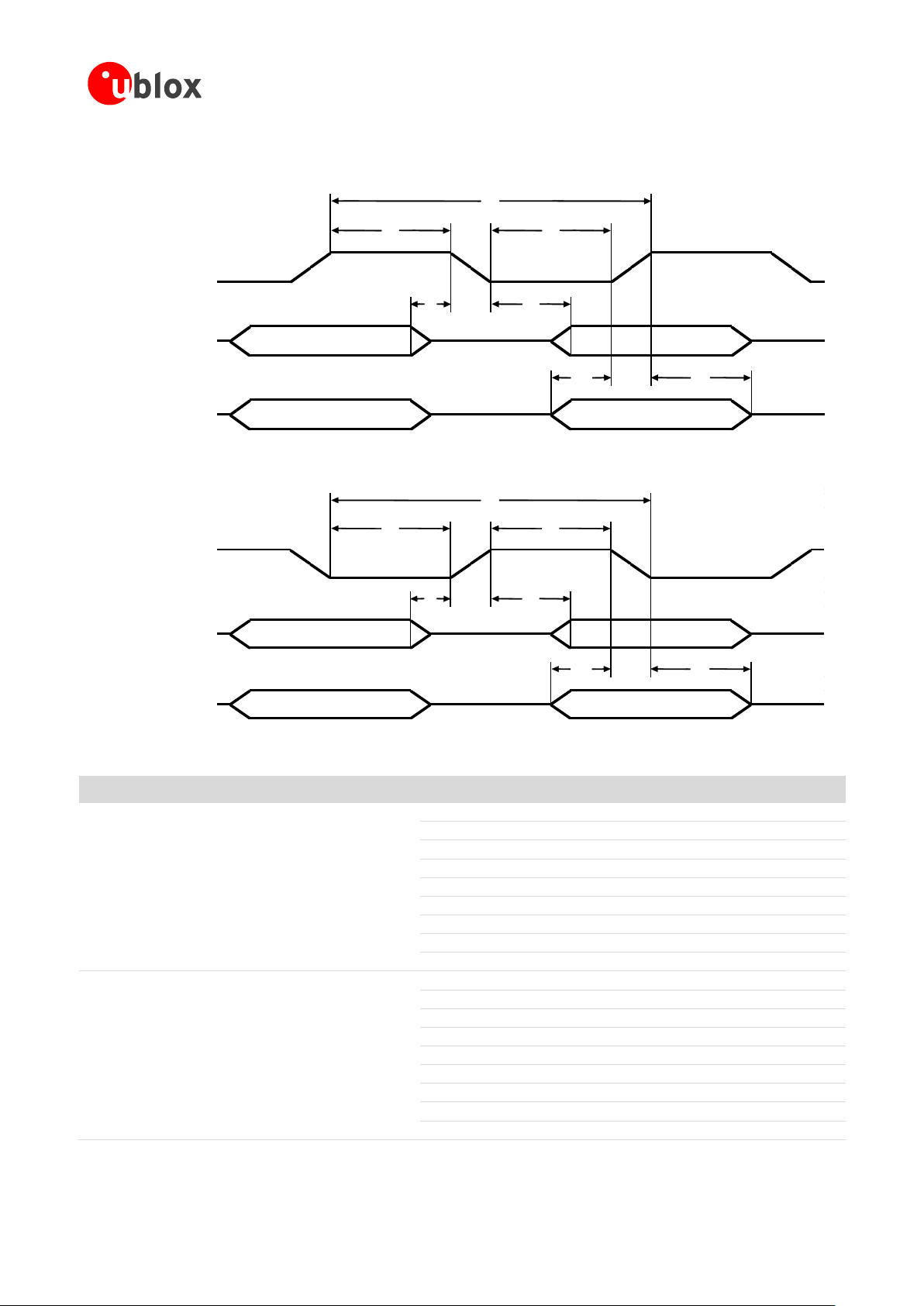
SARA-U2 series - Data Sheet
T7
T1
T2
T3
T4
T5
CLK
(Output)
TXD / WA
(Output)
RXD
(Input)
T6
CLK
(Output)
TXD / WA
(Output)
RXD
(Input)
T6
T7
T1
T2
T3
T4
T5
Parameter
Description
Min.
Typ.
Max.
Unit
Remarks
T1
I2S clock period
3.902
3.906
µs
<I2S_sample_rate>=0
2.830
2.834
µs
<I2S_sample_rate>=1
2.600
2.604
µs
<I2S_sample_rate>=2
1.949
1.953
µs
<I2S_sample_rate>=3
1.413
1.417
µs
<I2S_sample_rate>=4
1.298
1.302
µs
<I2S_sample_rate>=5
0.973
0.977
µs
<I2S_sample_rate>=6
0.705
0.709
µs
<I2S_sample_rate>=7
0.647
0.651
µs
<I2S_sample_rate>=8
1/T1
I2S clock frequency
256.0
256.3
kHz
<I2S_sample_rate>=0
352.8
353.3
kHz
<I2S_sample_rate>=1
384.0
384.6
kHz
<I2S_sample_rate>=2
512.0
513.1
kHz
<I2S_sample_rate>=3
705.6
707.6
kHz
<I2S_sample_rate>=4
768.0
770.4
kHz
<I2S_sample_rate>=5
1024
1028
kHz
<I2S_sample_rate>=6
1411
1419
kHz
<I2S_sample_rate>=7
1536
1545
kHz
<I2S_sample_rate>=8
Normal I2S mode – Master mode
Figure 5: AC characteristics of digital audio interface in Normal I2S mode (<I2S_mode> = 2,4,6,8,10,12) and Master mode enabled
Figure 6: AC characteristics of digital audio interface in Normal I2S mode (<I2S_mode> = 3,5,7,9,11,13) and Master mode enabled
UBX-13005287 - R19 Electrical specifications
Page 32 of 57
Page 33

SARA-U2 series - Data Sheet
Parameter
Description
Min.
Typ.
Max.
Unit
Remarks
T2
I2S clock high time
1.933
1.953
µs
<I2S_sample_rate>=0
1.397
1.417
µs
<I2S_sample_rate>=1
1.282
1.302
µs
<I2S_sample_rate>=2
0.957
0.977
µs
<I2S_sample_rate>=3
0.689
0.709
µs
<I2S_sample_rate>=4
0.631
0.651
µs
<I2S_sample_rate>=5
0.468
0.488
µs
<I2S_sample_rate>=6
0.334
0.354
µs
<I2S_sample_rate>=7
0.306
0.326
µs
<I2S_sample_rate>=8
T3
I2S clock low time
1.933
1.953
µs
<I2S_sample_rate>=0
1.397
1.417
µs
<I2S_sample_rate>=1
1.282
1.302
µs
<I2S_sample_rate>=2
0.957
0.977
µs
<I2S_sample_rate>=3
0.689
0.709
µs
<I2S_sample_rate>=4
0.631
0.651
µs
<I2S_sample_rate>=5
0.468
0.488
µs
<I2S_sample_rate>=6
0.334
0.354
µs
<I2S_sample_rate>=7
0.306
0.326
µs
<I2S_sample_rate>=8
I2S word alignment period
125.0
µs
<I2S_sample_rate>=0
90.70
µs
<I2S_sample_rate>=1
83.33
µs
<I2S_sample_rate>=2
62.50
µs
<I2S_sample_rate>=3
45.35
µs
<I2S_sample_rate>=4
41.67
µs
<I2S_sample_rate>=5
31.25
µs
<I2S_sample_rate>=6
22.68
µs
<I2S_sample_rate>=7
20.83
µs
<I2S_sample_rate>=8
I2S word alignment frequency
8.000
kHz
<I2S_sample_rate>=0
11.03
kHz
<I2S_sample_rate>=1
12.00
kHz
<I2S_sample_rate>=2
16.00
kHz
<I2S_sample_rate>=3
22.05
kHz
<I2S_sample_rate>=4
24.00
kHz
<I2S_sample_rate>=5
32.00
kHz
<I2S_sample_rate>=6
44.10
kHz
<I2S_sample_rate>=7
48.00
kHz
<I2S_sample_rate>=8
T4
I2S TXD invalid before I2S CLK high end
(before shifting edge of I2S CLK)
24
ns
<I2S_mode> = 2,4,6,8,10,12
I2S TXD invalid before I2S CLK low end
(before shifting edge of I2S CLK)
24
ns
<I2S_mode> = 3,5,7,9,11,13
T5
I2S TXD valid after I2S CLK low begin
(after shifting edge of I2S CLK)
32
ns
<I2S_mode> = 2,4,6,8,10,12
I2S TXD valid after I2S CLK high begin
(after shifting edge of I2S CLK)
32
ns
<I2S_mode> = 3,5,7,9,11,13
T6
I2S RXD setup time before I2S CLK low end
(before latching edge of I2S CLK)
60
ns
<I2S_mode> = 2,4,6,8,10,12
I2S RXD setup time before I2S CLK high end
(before latching edge of I2S CLK)
60
ns
<I2S_mode> = 3,5,7,9,11,13
T7
I2S RXD hold time after I2S CLK high begin
(after latching edge of I2S CLK)
10
ns
<I2S_mode> = 2,4,6,8,10,12
I2S RXD hold time after I2S CLK low begin
(after latching edge of I2S CLK)
10
ns
<I2S_mode> = 3,5,7,9,11,13
Table 20: AC characteristics of digital audio interface in Normal I2S mode and Master mode enabled
UBX-13005287 - R19 Electrical specifications
Page 33 of 57
Page 34
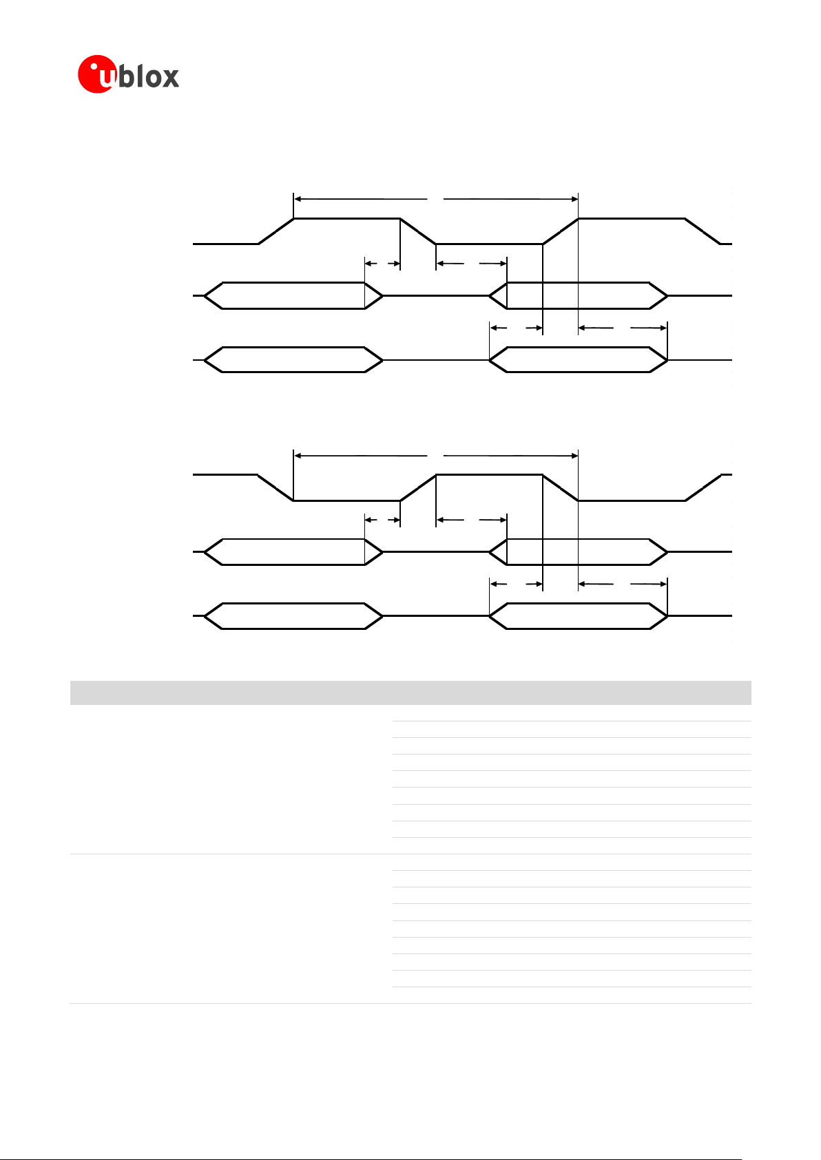
SARA-U2 series - Data Sheet
CLK
(Input)
TXD
(Output)
RXD / WA
(Input)
T6
T7
T1
T4
T5
T7
T1
T4
T5
CLK
(Input)
TXD
(Output)
RXD / WA
(Input)
T6
Parameter
Description
Min.
Typ.
Max.
Unit
Remarks
T1
I2S clock period
3.906
µs
<I2S_sample_rate>=0
2.834
µs
<I2S_sample_rate>=1
2.604
µs
<I2S_sample_rate>=2
1.953
µs
<I2S_sample_rate>=3
1.417
µs
<I2S_sample_rate>=4
1.302
µs
<I2S_sample_rate>=5
0.977
µs
<I2S_sample_rate>=6
0.709
µs
<I2S_sample_rate>=7
0.651
µs
<I2S_sample_rate>=8
1/T1
I2S clock frequency
256.0
kHz
<I2S_sample_rate>=0
352.8
kHz
<I2S_sample_rate>=1
384.0
kHz
<I2S_sample_rate>=2
512.0
kHz
<I2S_sample_rate>=3
705.6
kHz
<I2S_sample_rate>=4
768.0
kHz
<I2S_sample_rate>=5
1024
kHz
<I2S_sample_rate>=6
1411
kHz
<I2S_sample_rate>=7
1536
kHz
<I2S_sample_rate>=8
Normal I2S mode – Slave mode
Figure 7: AC characteristics of digital audio interface in Normal I2S mode (<I2S_mode> = 2,4,6,8,10,12) and Slave mode enabled
Figure 8: AC characteristics of digital audio interface in Normal I2S mode (<I2S_mode> = 3,5,7,9,11,13) and Slave mode enabled
UBX-13005287 - R19 Electrical specifications
Page 34 of 57
Page 35

SARA-U2 series - Data Sheet
Parameter
Description
Min.
Typ.
Max.
Unit
Remarks
I2S word alignment period
125.0
µs
<I2S_sample_rate>=0
90.70
µs
<I2S_sample_rate>=1
83.33
µs
<I2S_sample_rate>=2
62.50
µs
<I2S_sample_rate>=3
45.35
µs
<I2S_sample_rate>=4
41.67
µs
<I2S_sample_rate>=5
31.25
µs
<I2S_sample_rate>=6
22.68
µs
<I2S_sample_rate>=7
20.83
µs
<I2S_sample_rate>=8
I2S word alignment frequency
8.000
kHz
<I2S_sample_rate>=0
11.03
kHz
<I2S_sample_rate>=1
12.00
kHz
<I2S_sample_rate>=2
16.00
kHz
<I2S_sample_rate>=3
22.05
kHz
<I2S_sample_rate>=4
24.00
kHz
<I2S_sample_rate>=5
32.00
kHz
<I2S_sample_rate>=6
44.10
kHz
<I2S_sample_rate>=7
48.00
kHz
<I2S_sample_rate>=8
T4
I2S TXD invalid before I2S CLK falling edge
(before shifting edge of I2S CLK)
24
ns
<I2S_mode> = 2,4,6,8,10,12
I2S TXD invalid before I2S CLK rising edge
(before shifting edge of I2S CLK)
24
ns
<I2S_mode> = 3,5,7,9,11,13
T5
I2S TXD valid after I2S CLK falling edge
(after shifting edge of I2S CLK)
32
ns
<I2S_mode> = 2,4,6,8,10,12
I2S TXD valid after I2S CLK rising edge
(after shifting edge of I2S CLK)
32
ns
<I2S_mode> = 3,5,7,9,11,13
T6
I2S RXD setup time before I2S CLK rising edge
(before latching edge of I2S CLK)
60
ns
<I2S_mode> = 2,4,6,8,10,12
I2S RXD setup time before I2S CLK falling edge
(before latching edge of I2S CLK)
60
ns
<I2S_mode> = 3,5,7,9,11,13
T7
I2S RXD hold time after I2S CLK rising edge
(after latching edge of I2S CLK)
10
ns
<I2S_mode> = 2,4,6,8,10,12
I2S RXD hold time after I2S CLK falling edge
(after latching edge of I2S CLK)
10
ns
<I2S_mode> = 3,5,7,9,11,13
Table 21: AC characteristics of digital audio interface in Normal I2S mode and Slave mode enabled
UBX-13005287 - R19 Electrical specifications
Page 35 of 57
Page 36
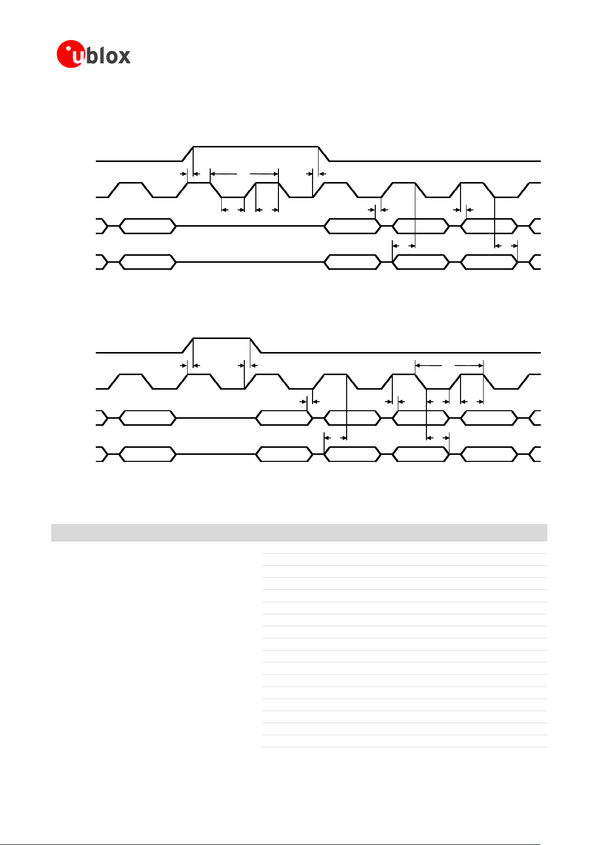
SARA-U2 series - Data Sheet
T4 T5
T6 T7
T8
T9
LSB
LSB
MSB
MSB
WA
(Output)
CLK
(Output)
TXD
(Output)
RXD
(Input)
T1
T2
T3
T4 T5
T6 T7
WA
(Output)
CLK
(Output)
LSB
MSB
MSB
LSB
TXD
(Output)
RXD
(Input)
T8
T9
T1
T2
T3
Parameter
Description
Min.
Typ.
Max.
Unit
Remarks
T1
I2S clock period
6.940
6.944
µs
<I2S_mode>=0, <I2S_sample_rate>=0
7.349
7.353
µs
<I2S_mode>=1, <I2S_sample_rate>=0
5.035
5.039
µs
<I2S_mode>=0, <I2S_sample_rate>=1
5.331
5.335
µs
<I2S_mode>=1, <I2S_sample_rate>=1
4.626
4.630
µs
<I2S_mode>=0, <I2S_sample_rate>=2
4.898
4.902
µs
<I2S_mode>=1, <I2S_sample_rate>=2
3.468
3.472
µs
<I2S_mode>=0, <I2S_sample_rate>=3
3.672
3.676
µs
<I2S_mode>=1, <I2S_sample_rate>=3
2.516
2.520
µs
<I2S_mode>=0, <I2S_sample_rate>=4
2.664
2.668
µs
<I2S_mode>=1, <I2S_sample_rate>=4
2.311
2.315
µs
<I2S_mode>=0, <I2S_sample_rate>=5
2.447
2.451
µs
<I2S_mode>=1, <I2S_sample_rate>=5
1.732
1.736
µs
<I2S_mode>=0, <I2S_sample_rate>=6
1.834
1.838
µs
<I2S_mode>=1, <I2S_sample_rate>=6
1.256
1.260
µs
<I2S_mode>=0, <I2S_sample_rate>=7
1.330
1.334
µs
<I2S_mode>=1, <I2S_sample_rate>=7
1.153
1.157
µs
<I2S_mode>=0, <I2S_sample_rate>=8
PCM mode – Master mode
Figure 9: AC characteristics of digital audio interface in PCM mode (<I2S_mode> = 0) and Master mode enabled
Figure 10: AC characteristics of digital audio interface in PCM mode (<I2S_mode> = 1) and Master mode enabled
UBX-13005287 - R19 Electrical specifications
Page 36 of 57
Page 37

SARA-U2 series - Data Sheet
Parameter
Description
Min.
Typ.
Max.
Unit
Remarks
1.221
1.225
µs
<I2S_mode>=1, <I2S_sample_rate>=8
1/T1
I2S clock frequency
144.0
144.1
kHz
<I2S_mode>=0, <I2S_sample_rate>=0
136.0
136.1
kHz
<I2S_mode>=1, <I2S_sample_rate>=0
198.5
198.6
kHz
<I2S_mode>=0, <I2S_sample_rate>=1
187.4
187.6
kHz
<I2S_mode>=1, <I2S_sample_rate>=1
216.0
216.2
kHz
<I2S_mode>=0, <I2S_sample_rate>=2
204.0
204.2
kHz
<I2S_mode>=1, <I2S_sample_rate>=2
288.0
288.3
kHz
<I2S_mode>=0, <I2S_sample_rate>=3
272.0
272.3
kHz
<I2S_mode>=1, <I2S_sample_rate>=3
396.9
397.5
kHz
<I2S_mode>=0, <I2S_sample_rate>=4
374.9
375.4
kHz
<I2S_mode>=1, <I2S_sample_rate>=4
432.0
432.7
kHz
<I2S_mode>=0, <I2S_sample_rate>=5
408.0
408.7
kHz
<I2S_mode>=1, <I2S_sample_rate>=5
576.0
577.3
kHz
<I2S_mode>=0, <I2S_sample_rate>=6
544.0
545.2
kHz
<I2S_mode>=1, <I2S_sample_rate>=6
793.8
796.3
kHz
<I2S_mode>=0, <I2S_sample_rate>=7
749.7
752.0
kHz
<I2S_mode>=1, <I2S_sample_rate>=7
864.0
867.0
kHz
<I2S_mode>=0, <I2S_sample_rate>=8
816.0
818.7
kHz
<I2S_mode>=1, <I2S_sample_rate>=8
T2
I2S clock low time
3.452
3.472
µs
<I2S_mode>=0, <I2S_sample_rate>=0
3.656
3.676
µs
<I2S_mode>=1, <I2S_sample_rate>=0
2.500
2.520
µs
<I2S_mode>=0, <I2S_sample_rate>=1
2.648
2.668
µs
<I2S_mode>=1, <I2S_sample_rate>=1
2.295
2.315
µs
<I2S_mode>=0, <I2S_sample_rate>=2
2.431
2.451
µs
<I2S_mode>=1, <I2S_sample_rate>=2
1.716
1.736
µs
<I2S_mode>=0, <I2S_sample_rate>=3
1.818
1.838
µs
<I2S_mode>=1, <I2S_sample_rate>=3
1.240
1.260
µs
<I2S_mode>=0, <I2S_sample_rate>=4
1.314
1.334
µs
<I2S_mode>=1, <I2S_sample_rate>=4
1.137
1.157
µs
<I2S_mode>=0, <I2S_sample_rate>=5
1.205
1.225
µs
<I2S_mode>=1, <I2S_sample_rate>=5
0.848
0.868
µs
<I2S_mode>=0, <I2S_sample_rate>=6
0.899
0.919
µs
<I2S_mode>=1, <I2S_sample_rate>=6
0.610
0.630
µs
<I2S_mode>=0, <I2S_sample_rate>=7
0.647
0.667
µs
<I2S_mode>=1, <I2S_sample_rate>=7
0.559
0.579
µs
<I2S_mode>=0, <I2S_sample_rate>=8
0.593
0.613
µs
<I2S_mode>=1, <I2S_sample_rate>=8
T3
I2S clock high time
3.452
3.472
µs
<I2S_mode>=0, <I2S_sample_rate>=0
3.656
3.676
µs
<I2S_mode>=1, <I2S_sample_rate>=0
2.500
2.520
µs
<I2S_mode>=0, <I2S_sample_rate>=1
2.648
2.668
µs
<I2S_mode>=1, <I2S_sample_rate>=1
2.295
2.315
µs
<I2S_mode>=0, <I2S_sample_rate>=2
2.431
2.451
µs
<I2S_mode>=1, <I2S_sample_rate>=2
1.716
1.736
µs
<I2S_mode>=0, <I2S_sample_rate>=3
1.818
1.838
µs
<I2S_mode>=1, <I2S_sample_rate>=3
1.240
1.260
µs
<I2S_mode>=0, <I2S_sample_rate>=4
1.314
1.334
µs
<I2S_mode>=1, <I2S_sample_rate>=4
1.137
1.157
µs
<I2S_mode>=0, <I2S_sample_rate>=5
1.205
1.225
µs
<I2S_mode>=1, <I2S_sample_rate>=5
0.848
0.868
µs
<I2S_mode>=0, <I2S_sample_rate>=6
0.899
0.919
µs
<I2S_mode>=1, <I2S_sample_rate>=6
0.610
0.630
µs
<I2S_mode>=0, <I2S_sample_rate>=7
UBX-13005287 - R19 Electrical specifications
Page 37 of 57
Page 38

SARA-U2 series - Data Sheet
Parameter
Description
Min.
Typ.
Max.
Unit
Remarks
0.647
0.667
µs
<I2S_mode>=1, <I2S_sample_rate>=7
0.559
0.579
µs
<I2S_mode>=0, <I2S_sample_rate>=8
0.593
0.613
µs
<I2S_mode>=1, <I2S_sample_rate>=8
I2S word alignment period
125.0
µs
<I2S_sample_rate>=0
90.70
µs
<I2S_sample_rate>=1
83.33
µs
<I2S_sample_rate>=2
62.50
µs
<I2S_sample_rate>=3
45.35
µs
<I2S_sample_rate>=4
41.67
µs
<I2S_sample_rate>=5
31.25
µs
<I2S_sample_rate>=6
22.68
µs
<I2S_sample_rate>=7
20.83
µs
<I2S_sample_rate>=8
I2S word alignment frequency
8.000
kHz
<I2S_sample_rate>=0
11.03
kHz
<I2S_sample_rate>=1
12.00
kHz
<I2S_sample_rate>=2
16.00
kHz
<I2S_sample_rate>=3
22.05
kHz
<I2S_sample_rate>=4
24.00
kHz
<I2S_sample_rate>=5
32.00
kHz
<I2S_sample_rate>=6
44.10
kHz
<I2S_sample_rate>=7
48.00
kHz
<I2S_sample_rate>=8
T4
I2S CLK high begin to I2S WA high begin
-24 32
ns
<I2S_mode> = 0
T5
I2S CLK low end to I2S WA high end
-24 32
ns
<I2S_mode> = 0
T6
I2S TXD invalid before I2S CLK low end
24
ns
<I2S_mode> = 0
T7
I2S TXD valid after I2S CLK high begin
22
ns
<I2S_mode> = 0
T8
I2S RXD setup time before I2S CLK high end
60
ns
<I2S_mode> = 0
T9
I2S RXD hold time after I2S CLK low begin
12
ns
<I2S_mode> = 0
Table 22: AC characteristics of digital audio interface in PCM mode (<I2S_mode> = 0,1) and Master mode enabled
UBX-13005287 - R19 Electrical specifications
Page 38 of 57
Page 39
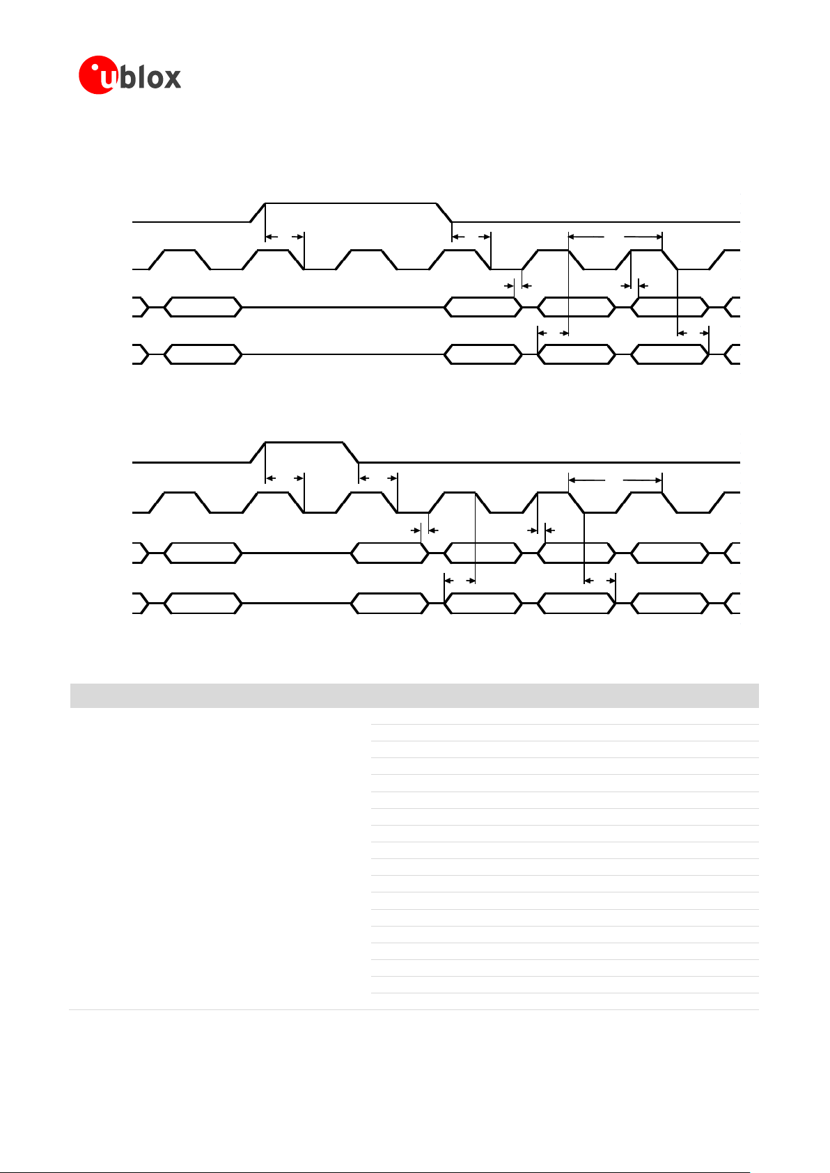
SARA-U2 series - Data Sheet
T4 T5
T6 T7
T8
T9
LSB
LSB
MSB
MSB
WA
(Input)
CLK
(Input)
TXD
(Output)
RXD
(Input)
T1
T4 T5
T6 T7
T8
T9
T1
LSB
MSB
MSB
LSB
TXD
(Output)
RXD
(Input)
WA
(Input)
CLK
(Input)
Parameter
Description
Min.
Typ.
Max.
Unit
Remarks
T1
I2S clock period
6.944
µs
<I2S_mode>=0, <I2S_sample_rate>=0
7.353
µs
<I2S_mode>=1, <I2S_sample_rate>=0
5.039
µs
<I2S_mode>=0, <I2S_sample_rate>=1
5.335
µs
<I2S_mode>=1, <I2S_sample_rate>=1
4.630
µs
<I2S_mode>=0, <I2S_sample_rate>=2
4.902
µs
<I2S_mode>=1, <I2S_sample_rate>=2
3.472
µs
<I2S_mode>=0, <I2S_sample_rate>=3
3.676
µs
<I2S_mode>=1, <I2S_sample_rate>=3
2.520
µs
<I2S_mode>=0, <I2S_sample_rate>=4
2.668
µs
<I2S_mode>=1, <I2S_sample_rate>=4
2.315
µs
<I2S_mode>=0, <I2S_sample_rate>=5
2.451
µs
<I2S_mode>=1, <I2S_sample_rate>=5
1.736
µs
<I2S_mode>=0, <I2S_sample_rate>=6
1.838
µs
<I2S_mode>=1, <I2S_sample_rate>=6
1.260
µs
<I2S_mode>=0, <I2S_sample_rate>=7
1.334
µs
<I2S_mode>=1, <I2S_sample_rate>=7
1.157
µs
<I2S_mode>=0, <I2S_sample_rate>=8
1.225
µs
<I2S_mode>=1, <I2S_sample_rate>=8
PCM mode – Slave mode
Figure 11: AC characteristics of digital audio interface in PCM mode (<I2S_mode> = 0) and Slave mode enabled
Figure 12: AC characteristics of digital audio interface in PCM mode (<I2S_mode> = 1) and Slave mode enabled
UBX-13005287 - R19 Electrical specifications
Page 39 of 57
Page 40

SARA-U2 series - Data Sheet
Parameter
Description
Min.
Typ.
Max.
Unit
Remarks
1/T1
I2S clock frequency
144.0
kHz
<I2S_mode>=0, <I2S_sample_rate>=0
136.0
kHz
<I2S_mode>=1, <I2S_sample_rate>=0
198.5
kHz
<I2S_mode>=0, <I2S_sample_rate>=1
187.4
kHz
<I2S_mode>=1, <I2S_sample_rate>=1
216.0
kHz
<I2S_mode>=0, <I2S_sample_rate>=2
204.0
kHz
<I2S_mode>=1, <I2S_sample_rate>=2
288.0
kHz
<I2S_mode>=0, <I2S_sample_rate>=3
272.0
kHz
<I2S_mode>=1, <I2S_sample_rate>=3
396.9
kHz
<I2S_mode>=0, <I2S_sample_rate>=4
374.9
kHz
<I2S_mode>=1, <I2S_sample_rate>=4
432.0
kHz
<I2S_mode>=0, <I2S_sample_rate>=5
408.0
kHz
<I2S_mode>=1, <I2S_sample_rate>=5
576.0
kHz
<I2S_mode>=0, <I2S_sample_rate>=6
544.0
kHz
<I2S_mode>=1, <I2S_sample_rate>=6
793.8
kHz
<I2S_mode>=0, <I2S_sample_rate>=7
749.7
kHz
<I2S_mode>=1, <I2S_sample_rate>=7
864.0
kHz
<I2S_mode>=0, <I2S_sample_rate>=8
816.0
kHz
<I2S_mode>=1, <I2S_sample_rate>=8
I2S word alignment period
125.0
µs
<I2S_sample_rate>=0
90.70
µs
<I2S_sample_rate>=1
83.33
µs
<I2S_sample_rate>=2
62.50
µs
<I2S_sample_rate>=3
45.35
µs
<I2S_sample_rate>=4
41.67
µs
<I2S_sample_rate>=5
31.25
µs
<I2S_sample_rate>=6
22.68
µs
<I2S_sample_rate>=7
20.83
µs
<I2S_sample_rate>=8
I2S word alignment frequency
8.000
kHz
<I2S_sample_rate>=0
11.03
kHz
<I2S_sample_rate>=1
12.00
kHz
<I2S_sample_rate>=2
16.00
kHz
<I2S_sample_rate>=3
22.05
kHz
<I2S_sample_rate>=4
24.00
kHz
<I2S_sample_rate>=5
32.00
kHz
<I2S_sample_rate>=6
44.10
kHz
<I2S_sample_rate>=7
48.00
kHz
<I2S_sample_rate>=8
T4
I2S WA high begin before I2S CLK low begin
(latching edge of I2S CLK)
36
ns
<I2S_mode>= 0
T5
I2S WA low begin before I2S CLK low begin
(latching edge of I2S CLK)
36
ns
<I2S_mode>= 0
T6
I2S TXD invalid before I2S CLK rising edge
(shifting edge of I2S CLK)
12
ns
<I2S_mode>= 0
T7
I2S TXD valid after I2S CLK rising edge
(shifting edge of I2S CLK)
79
ns
<I2S_mode>= 0
T8
I2S RXD setup time before I2S CLK falling edge
(latching edge of I2S CLK)
22
ns
<I2S_mode>= 0
T9
I2S RXD hold time after I2S CLK falling edge
(latching edge of I2S CLK)
24
ns
<I2S_mode>= 0
Table 23: AC characteristics of digital audio interface in PCM mode (<I2S_mode> = 0,1) and Slave mode enabled
UBX-13005287 - R19 Electrical specifications
Page 40 of 57
Page 41

T1
T2
T3
CODEC_CLK
(Output)
Parameter
Description
Min.
Typ.
Max.
Unit
Remarks
T1
CODEC_CLK clock period
38 ns
CODEC_CLK output set to 26 MHz
77 ns
CODEC_CLK output set to 13 MHz
1/T1
CODEC_CLK clock frequency
26 MHz
CODEC_CLK output set to 26 MHz
13 MHz
CODEC_CLK output set to 13 MHz
T2
CODEC_CLK clock low time
10
ns
CODEC_CLK output set to 26 MHz
26
ns
CODEC_CLK output set to 13 MHz
T3
CODEC_CLK clock high time
10
ns
CODEC_CLK output set to 26 MHz
26
ns
CODEC_CLK output set to 13 MHz
Parameter
Min.
Typ.
Max.
Unit
Remarks
USB detection voltage on pin VUSB_DET
4.40
5.00
5.25 V
Current sink at VUSB_DET
30 µA
High-speed squelch detection threshold (input differential
signal amplitude)
100 150
mV
High speed disconnect detection threshold (input differential
signal amplitude)
525 625
mV
High-speed data signaling input common mode voltage range
-50 500
mV
High-speed idle output level
-10 10
mV
High-speed data signaling output high level
360 440
mV High-speed data signaling output low level
-10 10
mV
Chirp J level (output differential voltage)
700 1100
mV
Chirp K level (output differential voltage)
-900 -500
mV
4.2.9.2 AC characteristics of Digital Clock Output pin
Figure 13: AC characteristics of CODEC_CLK digital clock output
SARA-U2 series - Data Sheet
Table 24: AC characteristics of CODEC_CLK digital clock output
4.2.10 USB pins
USB data lines (USB_D+ and USB_D-) are compliant to the USB 2.0 high-speed specification. See the Universal
Serial Bus Revision 2.0 specification [15] for detailed electrical characteristics. The values in Table 25 related to
USB 2.0 high-speed physical layer specifications are for information only.
Table 25: USB pins characteristics
UBX-13005287 - R19 Electrical specifications
Page 41 of 57
Page 42

SARA-U2 series - Data Sheet
Parameter
Min.
Typ.
Max.
Unit
Remarks
Internal supply for DDC domain
1.73
1.80
1.87 V Generic Digital Interfaces supply (V_INT)
L-level input
-0.20
0.35 V
H-level input
1.31 1.93 V
L-level output
0.00
0.35 V Max value at IOL = +1.0 mA
Input/Output leakage current
0.7
µA
0.2 V < VIN < 1.93 V
Clock frequency on SCL
100 kHz
4.2.11 DDC (I
2
C) pins
DDC (I2C) lines (SCL and SDA) are compliant to the I2C-bus standard mode specification. See the I2C-bus
Specifications [12] for detailed electrical characteristics. The values in Table 26 related to I2C-bus standard mode
specifications are for information only.
Table 26: DDC (I2C) pin characteristics (DDC domain)
UBX-13005287 - R19 Electrical specifications
Page 42 of 57
Page 43

C
R
R
P
Q
K M1 M1 M2
E
G
H1
J1
H2
J2
J2
H2
E
ANT pin
B
Pin 1
Indicator
K
G H1 J1
A
D D
O
O
L
N
L
I
F
F
Parameter
Description
Typical Tolerance
A
Module Height [mm]
26.0
(1023.6 mil)
+0.20/-0.20
(+7.9/-7.9 mil)
B
Module Width [mm]
16.0
(629.9 mil)
+0.20/-0.20
(+7.9/-7.9 mil)
C
Module Thickness [mm]
3.0
(118.4 mil)
+0.25/-0.15
(+9.8/-5.9 mil)
D
Horizontal Edge to Lateral Pin Pitch [mm]
2.0
(78.7 mil)
+0.20/-0.20
(+7.9/-7.9 mil)
E
Vertical Edge to Lateral Pin Pitch [mm]
2.5
(98.4 mil)
+0.20/-0.20
(+7.9/-7.9 mil)
F
Edge to Lateral Pin Pitch [mm]
1.05
(41.3 mil)
+0.20/-0.20
(+7.9/-7.9 mil)
G
Lateral Pin to Pin Pitch [mm]
1.1
(43.3 mil)
+0.02/-0.02
(+0.8/-0.8 mil)
H1
Lateral Pin Height [mm]
0.8
(31.5 mil)
+0.02/-0.02
(+0.8/-0.8 mil)
H2
Lateral Pin close to ANT Height [mm]
0.9
(35.4 mil)
+0.02/-0.02
(+0.8/-0.8 mil)
I
Lateral Pin Width [mm]
1.5
(59.1 mil)
+0.02/-0.02
(+0.8/-0.8 mil)
J1
Lateral Pin to Pin Distance [mm]
0.3
(11.8 mil)
+0.02/-0.02
(+0.8/-0.8 mil)
J2
Lateral Pin to Pin close to ANT Distance [mm]
0.2
(7.9 mil)
+0.02/-0.02
(+0.8/-0.8 mil)
K
Horizontal Edge to Central Pin Pitch [mm]
2.75
(108.3 mil)
+0.20/-0.20
(+7.9/-7.9 mil)
L
Vertical Edge to Central Pin Pitch [mm]
2.75
(108.3 mil)
+0.20/-0.20
(+7.9/-7.9 mil)
M1
Central Pin to Pin Horizontal Pitch [mm]
1.8
(70.9 mil)
+0.02/-0.02
(+0.8/-0.8 mil)
M2
Central Pin to Pin Horizontal Pitch [mm]
3.6
(141.7 mil)
+0.02/-0.02
(+0.8/-0.8 mil)
N
Central Pin to Pin Vertical Pitch [mm]
2.1
(82.7 mil)
+0.02/-0.02
(+0.8/-0.8 mil)
O
Central Pin Height and Width [mm]
1.1
(43.3 mil)
+0.02/-0.02
(+0.8/-0.8 mil)
P
Horizontal Edge to Pin 1 Indicator Pitch [mm]
0.9
(35.4 mil)
+0.20/-0.20
(+7.9/-7.9 mil)
Q
Vertical Edge to Pin 1 Indicator Pitch [mm]
1.0
(39.4 mil)
+0.20/-0.20
(+7.9/-7.9 mil)
R
Pin 1 Indicator Height and Width [mm]
0.6
(23.6 mil)
+0.02/-0.02
(+0.8/-0.8 mil)
Weight
Module Weight [g]
< 3
5 Mechanical specifications
SARA-U2 series - Data Sheet
Figure 14: SARA-U2 series module dimensions (bottom and side views)
Table 27: SARA-U2 series module dimensions
Module height tolerance +/–0.20 mm may be exceeded close to the corners of the PCB due to the cutting
process: in the worst case, the height could be +0.40 mm longer than the typical value.
For information regarding Footprint and Paste Mask, see the SARA-G3 and SARA-U2 series System
Integration Manual [6].
UBX-13005287 - R19 Mechanical specifications
Page 43 of 57
Page 44

SARA-U2 series - Data Sheet
Products marked with this lead-free symbol on the product label comply with the
"Directive 2002/95/EC of the European Parliament and the Council on the Restriction of
Use of certain Hazardous Substances in Electrical and Electronic Equipment" RoHS).
SARA-U2 modules are RoHS compliant.
No natural rubbers, hygroscopic materials, or materials containing asbestos are employed.
Certification Scheme
SARA-U201
SARA-U201
ATEX
SARA-U260
SARA-U270
SARA-U270
ATEX
SARA-U280
GCF (Global Certification Forum)
• • • •
PTCRB (PCS Type Certification
Review Board)
• • •
•
CE (Conformité Européenne)
• • • •
FCC (United States Federal
Communications Commission)
FCC identification number
•
XPY1CGM5NNN
•
XPY1CGM5NNN
•
XPYSARAU260
•
XPYSARAU280
ISED (Innovation, Science and
Economic Development, formerly
known as IC - Industry Canada)
ISED certification number
•
8595A-1CGM5NNN
•
8595A-1CGM5NNN
•
8595A-SARAU260
•
8595A-SARAU280
Anatel (Brazilian Certification)
• •
RCM (Australia Regulatory
Compliance Mark)
• • • •
Giteki (Japan approval mark)
• •
KCC (Korean KC mark)
• •
NCC (Taiwanese National
Communications Commission)
• •
CCC (China Compulsory
Certification)
• • • •
SRRC (State Radio Regulation of
China)
• • • •
AT&T (US Network Operator)
• • •
•
Rogers Canada (Canadian
Network Operator)
• •
KT (Korean Network Operator)
•
SKT (Korean Network Operator)
•
NTT DoCoMo (Japanese Network
Operator)
•
ATEX (ATmospheric EXplosives)
• •
6 Reliability tests and approvals
6.1 Reliability tests
Tests for product family qualifications are according to ISO 16750 “Road vehicles - Environmental conditions and
testing for electrical and electronic equipment“, and appropriate standards.
6.2 Approvals
6.2.1 SARA-U2 series
Table 28 lists the SARA-U2 series main approvals.
Table 28: SARA-U2 series main certification approvals
For all the certificates of compliancy and for the complete list of approvals (including country and network
operator approvals) of the SARA-U2 series modules, see our website (http://www.u-blox.com/) or please
contact the u-blox office or sales representative nearest you.
UBX-13005287 - R19 Reliability tests and approvals
Page 44 of 57
Page 45

SARA-U2 series - Data Sheet
SARA-U270 ATEX
Ui
3.8 V
Ii
1.6 A (burst)
Ci
132 µF
Li
9.8 µH
6.2.2 SARA-U201 ATEX and SARA-U270 ATEX
SARA-U201 ATEX and SARA-U270 ATEX modules are certified as components intended for use in potentially
explosive atmospheres compliant to the following standards:
IEC 60079-0: 2011
IEC 60079-11: 2011
IEC 60079-26: 2006
The certification numbers of the modules according to the ATEX directive 2014/34/EU are:
SARA-U201 ATEX: SIQ 16 ATEX 298 U
SARA-U270 ATEX: SIQ 15 ATEX 017 U
The certification numbers of the modules according to the IECEx conformity assessment system are:
SARA-U201 ATEX: IECEx SIQ 16.0006U
SARA-U270 ATEX: IECEx SIQ 15.0001U
According to the standards listed above, the modules are certified with the following marking:
SARA-U201 ATEX: Ex II 1G, Ex ia IIB
SARA-U270 ATEX: Ex II 1G, Ex ia IIC/IIB
According to the marking stated above, the modules are certified as electrical equipment of:
group ‘II’: intended for use in areas with explosive gas atmosphere other than mines susceptible to firedamp
category ‘1G’: intended for use in zone 0 hazardous areas, in which explosive atmospheres caused by
mixtures of air and gases, vapors or mists are present continuously, for long periods or frequently
level of protection ‘ia’: intrinsically safe apparatus with very high level of protection, not capable of causing
ignition in normal operation and with the application of one countable fault or a combination of any two
countable fault plus those non-countable faults which give the most onerous condition
subdivision ‘IIB’: intended for use in areas where the nature of the explosive gas atmosphere is considered
dangerous based on the Maximum Experimental Safe Gap or the Minimum Ignition Current ratio of the
explosive gas atmosphere in which the equipment may be installed (a typical gas is ethylene), so that the
modules are also suitable for applications intended for use in subdivision IIA (a typical gas is propane)
subdivision ‘IIC/IIB’: intended for use in areas where the nature of the explosive gas atmosphere is
considered very dangerous based on the Maximum Experimental Safe Gap or the Minimum Ignition Current
ratio of the explosive gas atmosphere in which the equipment may be installed (a typical gas is hydrogen), so
that the modules are also suitable for applications intended for use in subdivision IIB (typical gas is ethylene)
and subdivision IIA (a typical gas is propane)
Section 4.2.1 defines the temperature range of use for SARA-U201 ATEX and SARA-U270 ATEX modules.
The RF radiating profile of the modules is compliant to all the applicable 3GPP / ETSI standards, with a maximum
of 2 W RF pulse power (corresponding to 1.15 mJ RF pulse energy) and with a maximum average power of
250 mW according to the GSM/GPRS and WCDMA power class stated in Table 2. Section 9.1 describes the
nameplate of SARA-U201 ATEX and SARA-U270 ATEX modules (see Figure 19 and Figure 20).
The following maximum input and equivalent parameters must be considered in sub-division IIC:
UBX-13005287 - R19 Reliability tests and approvals
Page 45 of 57
Page 46

SARA-U2 series - Data Sheet
SARA-U201 ATEX
SARA-U270 ATEX
Ui
3.8
4.2
4.2
Ii
2.5 A (burst)
1.6 A (burst)
2.5 A (burst)
Ci
169 µF
169 µF
132 µF
Li
9.4 µH
9.4 µH
9.8 µH
The following maximum input and equivalent parameters must be considered in sub-divisions IIB, IIA (two
different configurations are allowed for SARA-U201 ATEX):
For more information about the integration of these modules in applications intended for use in
potentially explosive atmospheres, see the SARA-G3 / SARA-U2 Series System Integration Manual [6].
UBX-13005287 - R19 Reliability tests and approvals
Page 46 of 57
Page 47

SARA-U2 series - Data Sheet
Parameter
Specification
Reel type
B2
Delivery quantity
250
7 Product handling & soldering
7.1 Packaging
SARA-U2 modules are delivered as hermetically sealed, reeled tapes to enable efficient production, production
lot set-up and tear-down. For more information about packaging, see the u-blox Package Information
Guide [16].
Figure 15: Reeled SARA-U2 modules
7.1.1 Reels
SARA-U2 modules are deliverable in quantities of 250 pieces on a reel. SARA-U2 modules are delivered using
reel type B2 as described in the u-blox Package Information Guide [16].
Table 29: Reel information for SARA-U2 modules
Quantities of less than 250 pieces are also available. Contact u-blox for more information.
UBX-13005287 - R19 Product handling & soldering
Page 47 of 57
Page 48
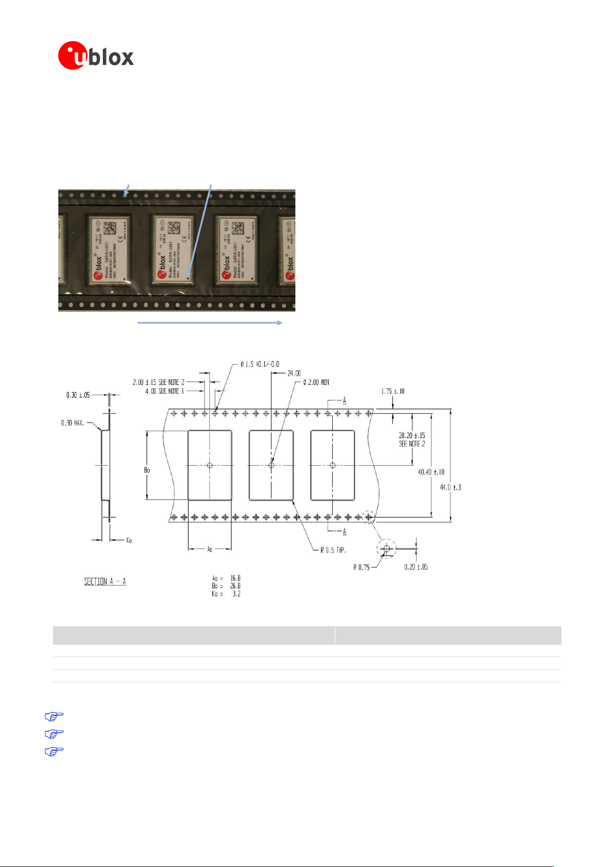
SARA-U2 series - Data Sheet
Pin 1Sprocket hole
Feed direction
Parameter
Typical value
Tolerance
Unit
A0
16.8
0.2
mm
B0
26.8
0.2
mm
K0
3.2
0.2
mm
7.1.2 Tapes
Figure 16 shows the position and the orientation of SARA-U2 series modules as they are delivered on the tape,
while Figure 17 and Table 30 specify the tape dimensions.
Figure 16: Orientation for SARA-U2 series modules on tape
Figure 17: SARA-U2 series tape dimensions (mm)
Table 30: SARA-U2 series tape dimensions (mm)
Note 1: 10 sprocket hole pitch cumulative tolerance ± 0.2 mm.
Note 2: pocket position relative to sprocket hole is measured as true position of pocket, not pocket hole.
Note 3: A
UBX-13005287 - R19 Product handling & soldering
Page 48 of 57
and B0 are calculated on a plane at a distance “R” above the bottom of the pocket.
0
Page 49
SARA-U2 series - Data Sheet
7.2 Moisture Sensitivity Levels
SARA-U2 modules are Moisture Sensitive Devices (MSD) in accordance to the IPC/JEDEC
specification.
The Moisture Sensitivity Level (MSL) relates to the packaging and handling precautions required. SARA-U2
modules are rated at MSL level 4. For more information regarding moisture sensitivity levels, labeling, storage
and drying, see the u-blox Package Information Guide [16].
For the MSL standard, see IPC/JEDEC J-STD-020 (can be downloaded from http://www.jedec.org/).
7.3 Reflow soldering
Reflow profiles are to be selected according to u-blox recommendations (see the SARA-G3 and SARA-U2 series
System Integration Manual [6]).
Failure to observe these recommendations can result in severe damage to the device!
7.4 ESD precautions
SARA-U2 modules contain highly sensitive electronic circuitry and are Electrostatic Sensitive
Devices (ESD). Handling SARA-U2 modules without proper ESD protection may destroy or
damage them permanently.
SARA-U2 modules are Electrostatic Sensitive Devices (ESD) and require special ESD precautions typically applied
to ESD sensitive components.
Table 8 details the maximum ESD ratings of the SARA-U2 module.
Proper ESD handling and packaging procedures must be applied throughout the processing, handling and
operation of any application that incorporates the SARA-U2 module.
ESD precautions should be implemented on the application board where the module is mounted, as described in
the SARA-G3 and SARA-U2 series System Integration Manual [6].
Failure to observe these precautions can result in severe damage to the device!
UBX-13005287 - R19 Product handling & soldering
Page 49 of 57
Page 50

Interface
AT settings
Comments
UART interface
Enabled
Multiplexing mode can be enabled by AT+CMUX command providing following channels:
Channel 0: control channel
Channel 1 – 5: AT commands / data connection
Channel 6: GNSS tunneling
Channel 7: SAP (SIM Access Profile)
AT+IPR=0
One-shot automatic baud rate detection enabled
AT+ICF=3,1
Frame format: 8 bits, no parity, 1 stop bit
Where AT+IPR=0 is the default value, the AT+ICF value in the profile is not
applied (AT+IPR=0 overrules the AT+ICF setting) and the one-shot automatic
frame detection is active.
AT&K3
HW flow control enabled
AT&S1
DSR line set ON in data mode and set OFF in command mode
AT&D1
Upon an ON-to-OFF transition of DTR, the module enters online command state and
issues an OK result code
AT&C1
Circuit 109 changes in accordance with the Carrier detect status; ON if the Carrier is
detected, OFF otherwise
AUX UART interface
Disabled
AT command interface is disabled by default on the AUX UART physical interface, and it
can be configured by AT+USIO command (see the u-blox AT Commands Manual [4])
USB interface
Enabled
7 USB CDCs (Communications Device Class) by default available:
USB1: AT and data
USB2: AT and data
USB3: AT and data
USB4: GNSS tunneling
USB5: Primary Log (diagnostic purpose)
USB6: Secondary Log (diagnostic purpose)
USB7: SAP (SIM Access Profile)
AT&K3
HW flow control enabled
AT&S1
DSR line set ON in data mode and set OFF in command mode
AT&D1
Upon an ON-to-OFF transition of DTR, the module enters online command state and
issues an OK result code
AT&C1
Circuit 109 changes in accordance with the Carrier detect status; ON if the Carrier is
detected, OFF otherwise
Power saving
AT+UPSV=0
Disabled
Network registration
AT+COPS=0
Self network registration
8 Default settings
SARA-U2 series - Data Sheet
Table 31: SARA-U2 series default settings
See the u-blox AT Commands Manual [4] and the SARA-G3 and SARA-U2 series System Integration Manual [6]
for information about further settings.
UBX-13005287 - R19 Default settings
Page 50 of 57
Page 51
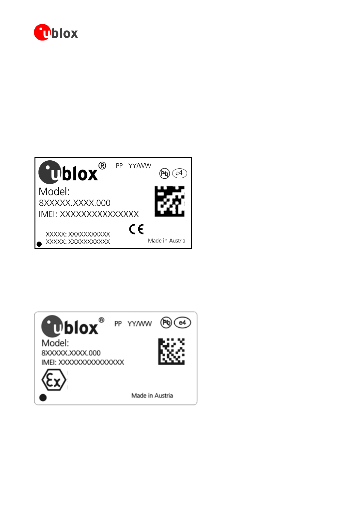
SARA-U2 series - Data Sheet
SARA-U2xx
xxx-xx
SARA-U201
03X-00
1304
SIQ 16 ATEX 298 U
IECEx SIQ 16.0006U
II 1G, Ex ia IIB
9 Labeling and ordering information
9.1 Product labeling
The labels of SARA-U2 series modules include important product information as described in this section.
Figure 18 illustrates the label of all the SARA-U2 series modules except for SARA-U201 ATEX and
SARA-U270 ATEX, and includes: u-blox logo, production lot, Pb-free marking, product Type Number, IMEI
number, and certification info and production country.
Figure 18: SARA-U2 series modules label
Figure 19 and Figure 20 illustrate the label of SARA-U201 ATEX and SARA-U270 ATEX modules respectively;
these include: u-blox logo, production lot, Pb-free marking, product Type Number, IMEI number, ATEX marking
with the IECEx and ATEX certificate numbers and category classification.
Figure 19: SARA-U201 ATEX modules label
UBX-13005287 - R19 Labeling and ordering information
Page 51 of 57
Page 52
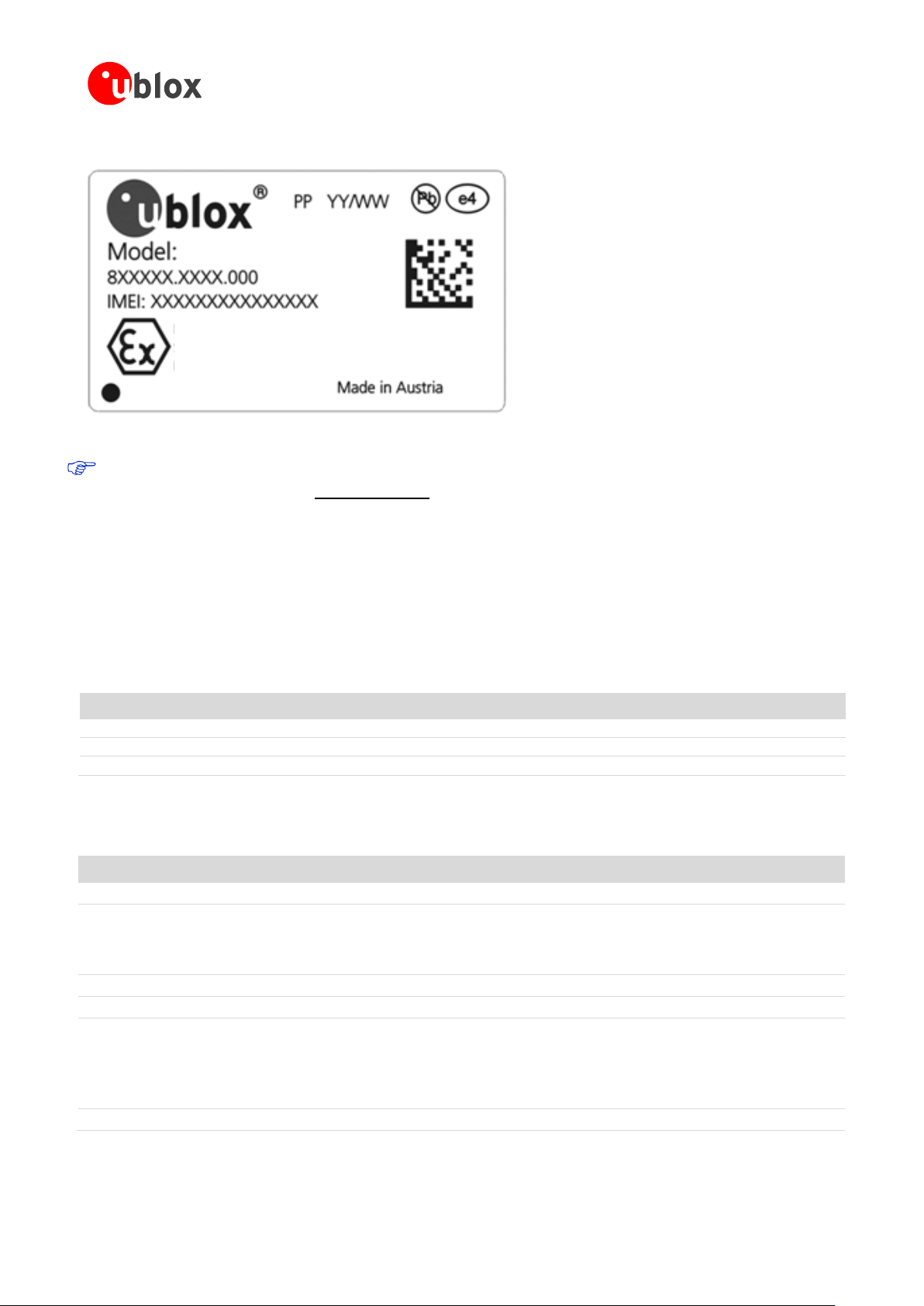
SARA-U2 series - Data Sheet
SIQ 15 ATEX 017 U
IECEx SIQ 15.0001U
II 1G Ex ia IIC/IIB
SARA-U270
00X-00
1304
Format
Structure
Product Name
SARA-TGVV
Ordering Code
SARA-TGVV-TTQ
Type Number
SARA-TGVV-TTQ-XX
Code
Meaning
Example
PPP(P)
Form factor (3 or 4 digit, typically 4 for cellular products)
SARA
TG
Platform (Technology and Generation)
Dominant technology: G: GSM/GPRS; U: UMTS/HSPA; C: CDMA 1xRTT; N: NB-IoT;
R: LTE low data rate (Cat 1 and below); L: LTE high data rate (Cat 3 and above)
Generation: 1…9
U2
VV
Variant function set based on the same platform [00…99]
00
TT
Major product version [00…99]
00
Q
Quality grade/production site
A = automotive
B = professional
S = professional
X = ATEX
S
XX
Minor product version (not relevant for certification)
Default value is 00
Figure 20: SARA-U270 ATEX modules label
For information about the approval codes and for all the certificates of compliancy of the SARA-U2 series
modules, see our website (www.u-blox.com) or contact the u-blox office or sales representative nearest
you.
9.2 Explanation of codes
Three different product code formats are used. The Product Name is used in documentation such as this data
sheet and identifies all the u-blox products, independent of packaging and quality grade. The Ordering Code
includes options and quality, while the Type Number includes the hardware and firmware versions. Table 32
details these 3 different formats:
Table 32: Product code formats
Table 33 explains the parts of the product code.
Table 33: Part identification code
UBX-13005287 - R19 Labeling and ordering information
Page 52 of 57
Page 53

Ordering No.
Product
SARA-U201-03B
UMTS/HSPA 800/850/900/1900/2100 MHz and GPRS/EDGE 850/900/1800/1900 MHz bands for worldwide use,
26.0 x 16.0 x 3.0 mm, 250 pcs/reel
SARA-U201-63B
UMTS/HSPA 800/850/900/1900/2100 MHz and GPRS/EDGE 850/900/1800/1900 MHz bands for worldwide use,
approved by NTT DoCoMo Japanese network operator
26.0 x 16.0 x 3.0 mm, 250 pcs/reel
SARA-U201-03X
UMTS/HSPA 800/850/900/1900/2100 MHz and GPRS/EDGE 850/900/1800/1900 MHz bands for worldwide use,
ATEX certified, 26.0 x 16.0 x 3.0 mm, 250 pcs/reel
SARA-U201-04B
UMTS/HSPA 800/850/900/1900/2100 MHz and GPRS/EDGE 850/900/1800/1900 MHz bands for worldwide use,
26.0 x 16.0 x 3.0 mm, 250 pcs/reel
SARA-U201-04X
UMTS/HSPA 800/850/900/1900/2100 MHz and GPRS/EDGE 850/900/1800/1900 MHz bands for worldwide use,
ATEX certified, 26.0 x 16.0 x 3.0 mm, 250 pcs/reel
SARA-U260-00S
UMTS/HSPA 850/1900 MHz and GSM/EGPRS 850/1900 MHz bands for America,
26.0 x 16.0 x 3.0 mm, 250 pcs/reel
SARA-U260-03S
UMTS/HSPA 850/1900 MHz and GSM/EGPRS 850/1900 MHz bands for America,
26.0 x 16.0 x 3.0 mm, 250 pcs/reel
SARA-U270-00S
UMTS/HSPA 900/2100 MHz and GSM/EGPRS 900/1800 MHz bands for Europe, Asia and other countries,
26.0 x 16.0 x 3.0 mm, 250 pcs/reel
SARA-U270-03S
UMTS/HSPA 900/2100 MHz and GSM/EGPRS 900/1800 MHz bands for Europe, Asia and other countries,
26.0 x 16.0 x 3.0 mm, 250 pcs/reel
SARA-U270-53S
UMTS/HSPA 900/2100 MHz bands, approved by KT Korean network operator,
26.0 x 16.0 x 3.0 mm, 250 pcs/reel
SARA-U270-73S
UMTS/HSPA 900/2100 MHz bands, approved by SKT Korean network operator,
26.0 x 16.0 x 3.0 mm, 250 pcs/reel
SARA-U270-00X
UMTS/HSPA 900/2100 MHz and GSM/EGPRS 900/1800 MHz bands for Europe, Asia and other countries,
ATEX certified, 26.0 x 16.0 x 3.0 mm, 250 pcs/reel
SARA-U280-00S
UMTS/HSPA 850/1900 MHz bands for America,
26.0 x 16.0 x 3.0 mm, 250 pcs/reel
SARA-U280-03S
UMTS/HSPA 850/1900 MHz bands for America,
26.0 x 16.0 x 3.0 mm, 250 pcs/reel
9.3 Ordering information
SARA-U2 series - Data Sheet
Table 34: Product ordering codes
UBX-13005287 - R19 Labeling and ordering information
Page 53 of 57
Page 54

Name
Definition
ACM
Abstract Control Model
ADC
Analog to Digital Converter
ATEX
Atmospheres Explosive
BER
Bit Error Rate
CDC
Communications Device Class
DDC
Display Data Channel (I2C compatible) Interface
DL
Down-link (Reception)
Driver Class
Output Driver Class: see Table 19 for definition
DRX
Discontinuous Reception
ECM
Ethernet networking Control Model
EDGE
Enhanced Data rates for GSM Evolution
ERS
External Reset Input Signal
GDI
Generic Digital Interfaces (V_INT supply power domain)
GND
Ground
GNSS
Global Navigation Satellite System
GPIO
General Purpose Input Output
GPRS
General Packet Radio Service
GSM
Global System for Mobile communications
H
High logic digital level
HSDPA
High Speed Downlink Packet Access
HSUPA
High Speed Uplink Packet Access
I2C
Inter-Integrated Circuit Interface
I2S
Inter-IC Sound Interface
L
Low logic digital level
LGA
Land Grid Array
N/A
Not Applicable
PCN / IN
Product Change Notification / Information Note
PD
Pull-Down
POS
Power-On Input Signal (power domain)
PU
Pull-Up
PU/PD Class
Pull-Up / Pull-Down Class: see Table 19 for definition
RMC
Reference Measurement Channel
SIM
SIM Interface (power domain)
SPI
Serial Peripheral Interface
T
Tristate (Output of the pin set to tri-state, i.e. high impedance state)
T/PD
Tristate with internal active Pull-Down enabled
T/PU
Tristate with internal active Pull-Up enabled
TBD
To Be Defined
UART
Universal Asynchronous Receiver-Transmitter serial interface
UL
Up-link (Transmission)
UMTS
Universal Mobile Telecommunications System
USB
Universal Serial Bus (power domain)
Appendix
A Glossary
SARA-U2 series - Data Sheet
Table 35: Explanation of abbreviations and terms used
UBX-13005287 - R19 Appendix
Page 54 of 57
Page 55

SARA-U2 series - Data Sheet
Related documents
[1] 3GPP TS 27.007 - AT command set for User Equipment (UE)
[2] 3GPP TS 27.005 - Use of Data Terminal Equipment - Data Circuit terminating Equipment (DTE - DCE)
interface for Short Message Service (SMS) and Cell Broadcast Service (CBS)
[3] 3GPP TS 27.010 - Terminal Equipment to User Equipment (TE-UE) multiplexer protocol
[4] u-blox AT Commands Manual, document number UBX-13002752
[5] u-blox Android RIL Production delivery Application note, document number UBX-13002041
[6] u-blox SARA-G3 and SARA-U2 series System Integration Manual, document number UBX-13000995
[7] u-blox GNSS Implementation Application Note, document number UBX-13001849
[8] 3GPP TS 26.267 eCall Data Transfer; In-band modem solution; General description
[9] 3GPP TS44.031 Location Services (LCS); Mobile Station (MS) - Serving Mobile Location Centre (SMLC)
Radio Resource LCS Protocol (RRLP)
[10] ITU-T Recommendation V24, 02-2000. List of definitions for interchange circuits between Data
Terminal Equipment (DTE) and Data Connection Equipment (DCE)
[11] u-blox Mux Implementation Application Note for wireless modules, document number UBX-13001887
[12] I
[13] 3GPP TS 34.121-1 - User Equipment conformance specification; Radio transmission and reception
[14] 3GPP TS 51.010-1 - Mobile Station conformance specification; Part 1: Conformance specification
[15] Universal Serial Bus Revision 2.0 specification, http://www.usb.org/developers/docs/usb20_docs/
[16] u-blox Package Information Guide, document number UBX-14001652
[17] 3GPP TS 25.331 Radio Resource Control (RRC); Protocol specification
[18] GSMA IoT Device Connection Efficiency Guidelines
For regular updates to u-blox documentation and to receive product change notifications, register on our
2
C-bus specification and user manual - Rev. 5 - 9 October 2012 - NXP Semiconductors,
http://www.nxp.com/documents/user_manual/UM10204.pdf
(FDD); Part 1: Conformance specification
homepage.
UBX-13005287 - R19 Related documents
Page 55 of 57
Page 56
Revision
Date
Name
Comments
R01
22-Jan-2014
sfal / sses
Initial release
R02
29-Apr-2014
sses
Updated: receiver sensitivity performance, normal operating temperature range,
maximum ESD ratings, USB audio device class support, GPIO configuration table.
R03
20-Jun-2014
sses
Advance Information document status.
Added VCC current consumption characteristics.
R04
18-Jul-2014
sses
Early Production Information document status.
Added VCC current consumption characteristics for 3G Tx/Rx connected modes.
R05
10-Apr-2015
sfal
Extended the document applicability to SARA-U270 ATEX; removed SARA-U290
and audio over USB feature; updated list of approvals and product labeling
R06
15-May-2015
sfal
Extended applicability to product version “03” and related features
R07
26-Jun-2015
lpah
Advance Information document status.
R08
10-Aug-2015
sfal
Early Production Information document status
Extended applicability to SARA-U270-53S
R09
02-Dec-2015
sses
Document status reverted to Objective Specification
Extended applicability to SARA-U201-03A and SARA-U201-03B
R10
25-May-2016
lpah / sfal
Added SARA-U260-00S-01, SARA-U270-00S-01
Removed SARA-U260-00S-00
Added SARA-U201 ATEX and updated SARA-U201 electrical specification values
R11
08-Jul-2016
lpah / sfal
Document status updated to Advance Information
R12
30-Aug-2016
lpah
Document status updated to Early Production
R13
07-Oct-2016
lpah
Document status reverted to Advance Information
Extended applicability to SARA-U270-73S
Removed the applicability to SARA-U201-03A
R14
14-Dec-2016
lpah
"Disclosure restriction" replaces "Document status" on page 2 and document
footer
R15
03-Aug-2017
lpah
Extended applicability to SARA-U270-53S-01
Updated label and approvals information
R16
20-Sep-2017
lpah / sses
Extended applicability to SARA-U201 modules "63" and "04" product versions
R17
31-Oct-2017
lpah / sses
Updated SARA-U201-04B / SARA-U201-04X product status
R18
02-Jan-2018
lpah
Extended document applicability to new SARA-U2 type numbers
R19
26-Feb-2018
lpah
Updated product status of new SARA-U2 type numbers
Extended document applicability to SARA-U201-63B-01.
Revision history
SARA-U2 series - Data Sheet
UBX-13005287 - R19 Revision history
Page 56 of 57
Page 57

u-blox Offices
North, Central and South America
u-blox America, Inc.
Phone: +1 703 483 3180
E-mail: info_us@u-blox.com
Regional Office West Coast:
Phone: +1 408 573 3640
E-mail: info_us@u-blox.com
Technical Support:
Phone: +1 703 483 3185
E-mail: support_us@u-blox.com
Headquarters
Europe, Middle East, Africa
u-blox AG
Phone: +41 44 722 74 44
E-mail: info@u-blox.com
Support: support@u-blox.com
Asia, Australia, Pacific
u-blox Singapore Pte. Ltd.
Phone: +65 6734 3811
E-mail: info_ap@u-blox.com
Support: support_ap@u-blox.com
Regional Office Australia:
Phone: +61 2 8448 2016
E-mail: info_anz@u-blox.com
Support: support_ap@u-blox.com
Regional Office China (Beijing):
Phone: +86 10 68 133 545
E-mail: info_cn@u-blox.com
Support: support_cn@u-blox.com
Regional Office China (Chongqing):
Phone: +86 23 6815 1588
E-mail: info_cn@u-blox.com
Support: support_cn@u-blox.com
Regional Office China (Shanghai):
Phone: +86 21 6090 4832
E-mail: info_cn@u-blox.com
Support: support_cn@u-blox.com
Regional Office China (Shenzhen):
Phone: +86 755 8627 1083
E-mail: info_cn@u-blox.com
Support: support_cn@u-blox.com
Regional Office India:
Phone: +91 80 4050 9200
E-mail: info_in@u-blox.com
Support: support_in@u-blox.com
Regional Office Japan (Osaka):
Phone: +81 6 6941 3660
E-mail: info_jp@u-blox.com
Support: support_jp@u-blox.com
Regional Office Japan (Tokyo):
Phone: +81 3 5775 3850
E-mail: info_jp@u-blox.com
Support: support_jp@u-blox.com
Regional Office Korea:
Phone: +82 2 542 0861
E-mail: info_kr@u-blox.com
Support: support_kr@u-blox.com
Regional Office Taiwan:
Phone: +886 2 2657 1090
E-mail: info_tw@u-blox.com
Support: support_tw@u-blox.com
Contact
For complete contact information, visit us at http://www.u-blox.com/
SARA-U2 series - Data Sheet
UBX-13005287 - R19 Contact
Page 57 of 57
 Loading...