

Page 1

UBX-16029218 - R20
C1-Public www.u-blox.com
SARA-R4 series
Multi-band LTE-M / NB-IoT / EGPRS modules
System integration manual
Abstract
This document describes the features and the integration of the size-optimized SARA-R4 series
cellular modules. These modules are a complete, cost efficient, performance optimized, multi-mode
and multi band LTE-M / NB-IoT / EGPRS solution in the compact SARA form factor.
SARA-R4
Page 2

SARA-R4 series - System integration manual
UBX-16029218 - R20 Document information Page 2 of 128
C1-Public
Document information
Title
SARA-R4 series
Subtitle
Multi-band LTE-M / NB-IoT / EGPRS modules
Document type
System integration manual
Document number
UBX-16029218
Revision and date
R20
02-Apr-2021
Disclosure restriction
C1-Public
Product status
Corresponding content status
Functional sample
Draft
For functional testing. Revised and supplementary data will be published later.
In development /
Prototype
Objective specification
Target values. Revised and supplementary data will be published later.
Engineering sample
Advance information
Data based on early testing. Revised and supplementary data will be published later.
Initial production
Early production information
Data from product verification. Revised and supplementary data may be published later.
Mass production /
End of life
Production information
Document contains the final product specification.
This document applies to the following products:
Product name
Type number
Modem version
Application version
PCN reference
Product status
SARA-R410M
SARA-R410M-01B-00
L0.0.00.00.02.03
UBX-18059854
Obsolete
SARA-R410M-02B-00
L0.0.00.00.05.06
A02.00
UBX-18010263
Obsolete
L0.0.00.00.05.06
A02.01
UBX-18070443
Obsolete
SARA-R410M-02B-01
L0.0.00.00.05.08
A02.04
UBX-19041392
Mass production
SARA-R410M-02B-02
L0.0.00.00.05.11
A.02.16
UBX-20033274
Mass production
SARA-R410M-02B-03
L0.0.00.00.05.12
A.02.19
UBX-20058104
Initial production
SARA-R410M-52B-00
L0.0.00.00.06.05
A02.06
UBX-18045915
Obsolete
SARA-R410M-52B-01
L0.0.00.00.06.08
A02.11
UBX-19024506
Mass production
SARA-R410M-52B-02
L0.0.00.00.06.11
A.02.16
UBX-20033274
Mass production
SARA-R410M-63B-00
L0.08.12
A.01.11
UBX-20006293
End of life
SARA-R410M-63B-01
L0.08.12
A.01.12
UBX-20053055
Initial production
SARA-R410M-73B-00
L0.08.12
A.01.11
UBX-20006294
End of life
SARA-R410M-73B-01
L0.08.12
A.01.12
UBX-20049254
Initial production
SARA-R410M-83B-00
L0.08.12
A01.11
UBX-20027231
End of life
SARA-R410M-83B-01
L0.08.12
A.01.12
UBX-20049255
Initial production
SARA-R412M
SARA-R412M-02B-00
M0.09.00
A.02.11
UBX-19004091
Obsolete
SARA-R412M-02B-01
M0.10.00
A.02.14
UBX-19016568
Mass production
SARA-R412M-02B-02
M0.11.01
A.02.17
UBX-20031249
Mass production
SARA-R412M-02B-03
M0.12.00
A.02.19
UBX-20058105
Initial production
SARA-R422
SARA-R422-00B-00
00.10
A00.00
UBX-21007232
Engineering sample 2
SARA-R422S
SARA-R422S-00B-00
00.10
A00.00
UBX-21007232
Engineering sample 2
SARA-R422M8S
SARA-R422M8S-00B-00
00.10
A00.00
UBX-21007232
Engineering sample 2
u-blox or third parties may hold intellectual property rights in the products, names, logos and designs included in this document.
Copying, reproduction, modification or disclosure to third parties of this document or any part thereof is only permitted with the
express written permission of u-blox.
The information contained herein is provided “as is” and u-blox assumes no liability for its use. No warranty, either express or
implied, is given, including but not limited to, with respect to the accuracy, correctness, reliability and fitness for a particular
purpose of the information. This document may be revised by u-blox at any time without notice. For the most recent documents,
visit www.u-blox.com.
Copyright © u-blox AG.
Page 3

SARA-R4 series - System integration manual
UBX-16029218 - R20 Contents Page 3 of 128
C1-Public
Contents
Document information ................................................................................................................................ 2
Contents .......................................................................................................................................................... 3
1 System description ............................................................................................................................... 6
1.1 Overview ........................................................................................................................................................ 6
1.2 Architecture ...............................................................................................................................................10
1.3 Pin-out .........................................................................................................................................................13
1.4 Operating modes .......................................................................................................................................18
1.5 Supply interfaces ......................................................................................................................................21
1.5.1 Module supply input (VCC) .............................................................................................................21
1.5.2 Generic digital interfaces supply output (V_INT) .......................................................................27
1.6 System function interfaces ....................................................................................................................28
1.6.1 Module power-on ..............................................................................................................................28
1.6.2 Module power-off ..............................................................................................................................29
1.6.3 Module reset ......................................................................................................................................31
1.7 Antenna interfaces ...................................................................................................................................32
1.7.1 Cellular antenna RF interface (ANT) .............................................................................................32
1.7.2 GNSS antenna RF interface (ANT_GNSS) ...................................................................................33
1.7.3 Antenna detection interface (ANT_DET).....................................................................................34
1.8 SIM interface ..............................................................................................................................................34
1.8.1 SIM interface .....................................................................................................................................34
1.8.2 SIM detection interface ...................................................................................................................34
1.9 Data communication interfaces ............................................................................................................35
1.9.1 UART interfaces ................................................................................................................................35
1.9.2 USB interface .....................................................................................................................................37
1.9.3 SPI interface ......................................................................................................................................38
1.9.4 SDIO interface ...................................................................................................................................38
1.9.5 DDC (I2C) interface ...........................................................................................................................38
1.10 Audio ............................................................................................................................................................39
1.11 General Purpose Input/Output ...............................................................................................................39
1.12 GNSS peripheral input output ................................................................................................................40
1.13 Reserved pins (RSVD) ..............................................................................................................................40
2 Design-in ................................................................................................................................................ 41
2.1 Overview ......................................................................................................................................................41
2.2 Supply interfaces ......................................................................................................................................42
2.2.1 Module supply (VCC) ........................................................................................................................42
2.2.2 Generic digital interfaces supply output (V_INT) .......................................................................58
2.3 System functions interfaces ..................................................................................................................59
2.3.1 Module PWR_ON / PWR_CTRL input ............................................................................................59
2.3.2 Module RESET_N input ...................................................................................................................60
2.4 Antenna interfaces ...................................................................................................................................61
Page 4

SARA-R4 series - System integration manual
UBX-16029218 - R20 Contents Page 4 of 128
C1-Public
2.4.1 General guidelines for antenna interfaces ..................................................................................61
2.4.2 Cellular antenna RF interface (ANT) .............................................................................................65
2.4.3 GNSS antenna RF interface (ANT_GNSS) ...................................................................................68
2.4.4 Cellular and GNSS RF coexistence ................................................................................................72
2.4.5 Antenna detection interface (ANT_DET).....................................................................................75
2.5 SIM interface ..............................................................................................................................................78
2.5.1 Guidelines for SIM circuit design ...................................................................................................78
2.5.2 Guidelines for SIM layout design ...................................................................................................82
2.6 Data communication interfaces ............................................................................................................83
2.6.1 UART interface ..................................................................................................................................83
2.6.2 USB interface .....................................................................................................................................88
2.6.3 SPI interface ......................................................................................................................................91
2.6.4 SDIO interface ...................................................................................................................................91
2.6.5 DDC (I2C) interface ...........................................................................................................................91
2.7 Audio ............................................................................................................................................................94
2.7.1 Guidelines for Audio circuit design ................................................................................................94
2.8 General Purpose Input/Output ...............................................................................................................94
2.8.1 Guidelines for GPIO circuit design .................................................................................................94
2.8.2 Guidelines for general purpose input/output layout design ....................................................95
2.9 GNSS peripheral input output ................................................................................................................95
2.9.1 Guidelines for GNSS peripheral input output circuit design ....................................................95
2.9.2 Guidelines for GNSS peripheral input output layout design ....................................................95
2.10 Reserved pins (RSVD) ..............................................................................................................................96
2.11 Module placement ....................................................................................................................................96
2.12 Module footprint and paste mask .........................................................................................................97
2.13 Thermal guidelines ...................................................................................................................................98
2.14 Schematic for SARA-R4 series module integration ..........................................................................99
2.14.1 Schematic for SARA-R4 series modules .....................................................................................99
2.15 Design-in checklist ................................................................................................................................. 100
2.15.1 Schematic checklist ...................................................................................................................... 100
2.15.2 Layout checklist ............................................................................................................................. 100
2.15.3 Antenna checklist .......................................................................................................................... 101
3 Handling and soldering ................................................................................................................... 102
3.1 Packaging, shipping, storage and moisture preconditioning ....................................................... 102
3.2 Handling ................................................................................................................................................... 102
3.3 Soldering .................................................................................................................................................. 103
3.3.1 Soldering paste .............................................................................................................................. 103
3.3.2 Reflow soldering ............................................................................................................................. 103
3.3.3 Optical inspection .......................................................................................................................... 104
3.3.4 Cleaning ........................................................................................................................................... 104
3.3.5 Repeated reflow soldering ........................................................................................................... 105
3.3.6 Wave soldering ............................................................................................................................... 105
3.3.7 Hand soldering ............................................................................................................................... 105
Page 5

SARA-R4 series - System integration manual
UBX-16029218 - R20 Contents Page 5 of 128
C1-Public
3.3.8 Rework ............................................................................................................................................. 105
3.3.9 Conformal coating ......................................................................................................................... 105
3.3.10 Casting ............................................................................................................................................. 105
3.3.11 Grounding metal covers ............................................................................................................... 106
3.3.12 Use of ultrasonic processes ........................................................................................................ 106
4 Approvals ............................................................................................................................................. 107
4.1 Product certification approval overview ............................................................................................ 107
4.2 US Federal Communications Commission notice ........................................................................... 111
4.2.1 Safety warnings review the structure ....................................................................................... 111
4.2.2 Declaration of Conformity ............................................................................................................ 112
4.2.3 Modifications .................................................................................................................................. 113
4.3 Innovation, Science, Economic Development Canada notice ....................................................... 114
4.3.1 Declaration of Conformity ............................................................................................................ 114
4.3.2 Modifications .................................................................................................................................. 115
4.4 European Conformance CE mark ....................................................................................................... 116
4.5 National Communication Commission Taiwan ............................................................................... 117
4.6 ANATEL Brazil ........................................................................................................................................ 118
4.7 Australian Conformance ...................................................................................................................... 118
4.8 GITEKI Japan .......................................................................................................................................... 118
4.9 KC South Korea ...................................................................................................................................... 118
5 Product testing ................................................................................................................................. 119
5.1 u-blox in-series production test .......................................................................................................... 119
5.2 Test parameters for OEM manufacturers ........................................................................................ 120
5.2.1 “Go/No go” tests for integrated devices ................................................................................... 120
5.2.2 RF functional tests ........................................................................................................................ 120
Appendix ..................................................................................................................................................... 122
A Migration between SARA modules ............................................................................................. 122
B Glossary ............................................................................................................................................... 122
Related documentation ......................................................................................................................... 125
Revision history ........................................................................................................................................ 126
Contact ........................................................................................................................................................ 128
Page 6

SARA-R4 series - System integration manual
UBX-16029218 - R20 System description Page 6 of 128
C1-Public
1 System description
1.1 Overview
The SARA-R4 series modules are a multi-band LTE-M / NB-IoT / EGPRS multi-mode solution in the
miniature SARA LGA form factor (26.0 x 16.0 mm, 96-pin). They allow an easy integration into
compact designs and a seamless drop-in migration from other u-blox cellular module families.
SARA-R4 series modules provide software-based multi-band configurability enabling international
multi-regional coverage in LTE-M / NB-IoT and (E)GPRS radio access technologies.
SARA-R4 series modules offer data communications over an extended operating temperature range
of –40 °C to +85 °C, with low power consumption, and with coverage enhancement for deeper range
into buildings and basements (and underground with NB-IoT).
SARA-R4 series modules are form-factor compatible with the u-blox LISA, LARA and TOBY cellular
module families and are pin-to-pin compatible with the u-blox SARA-N, SARA-G and SARA-U cellular
module families. This facilitates migration from other u-blox LPWA, GSM/GPRS, CDMA, UMTS/HSPA
and higher LTE categories modules, maximizing customer investments, simplifying logistics, and
enabling very short time-to-market.
With many interface options and an integrated IP stack, SARA-R4 series modules are the optimal
choice for LPWA applications with low to medium data throughput rates, as well as devices that
require long battery lifetimes, such as used in smart metering, smart lighting, telematics, asset
tracking, remote monitoring, alarm panels, and connected health.
Secure cloud product versions are available within the SARA-R4 series modules, including a unique
and immutable root-of-trust. This provides the foundation for a trusted set of advanced security
functionalities. The scalable, pre-shared key management system offers best-in-class data
encryption and decryption, both on-device as well as from device-to-cloud. Utilizing the latest (D)TLS
stack and cipher suites with hardware-based crypto acceleration provides robust, efficient, and
protected communication.
Furthermore, the SARA-R422 series modules support a comprehensive set of 3GPP Rel. 14 features
for LTE Cat M1 and Cat NB2 that are relevant for IoT applications.
The dedicated SARA-R422M8S module is pre-integrated with the u-blox M8 GNSS receiver chip and
a separate GNSS antenna interface which provides highly reliable, accurate positioning data
simultaneously with LTE communication. In addition, the module offers unique hybrid positioning, in
which the GNSS position is enhanced with u-blox CellLocate® data, providing location always and
everywhere.
Customers can future-proof their solutions by means of Over-The-Air firmware updates, thanks to
the uFOTA client/server solution that utilizes LWM2M, a light and compact protocol ideal for IoT.
SARA-R4 series modules will also support VoLTE over Cat M1 and CSFB over 2G RAT. The flexibility
extends further through dynamic mode selection as M1-only/preferred or NB-IoT-only/preferred.
Page 7

SARA-R4 series - System integration manual
UBX-16029218 - R20 System description Page 7 of 128
C1-Public
Product version
Region
RAT
Positioning
Interfaces
Features
Grade
3GPP release baseline 3GPP L
TE category
LTE FDD
bands
(E)GPRS 4
-band
Integrated GNSS receiver External GNSS control via modem AssistNow software CellLocate® UART
USB
SPI
SDIO
DDC (I2C) GPIOs
I2S audio interface Security services Root of trust: secure element Ultra-low power consum
ption in PSM
Embedded TCP/UDP stack Embedded HTTPS, FTPS, TLS DTLS
FW update via serial u-blox Firmware update
Over the Air
(uFOTA) LwM2M device management MQTT / MQTT
-SN
Last gasp Jamming detection Antenna and SIM detection Standard Professional Automoti
ve
SARA-R410M-01B
North
America
13
M1
2,4
5,12
● ●
●
● ● ● ● ● ● ● ●
SARA-R410M-02B
Multi region
13
M1
NB1
*
● ● ● ● ●
●
●
● ● ● ● ● ● ● ● ● ●
SARA-R410M-52B
North
America
13
M1
2,4,5
12,13
●
● ●
●
●
●
● ● ● ● ● ● ● ● ● ●
SARA-R410M-63B
Japan
13
M1
1,8,19
● ● ● ● ●
●
● ● ● ● ● ● ● ● ● ● ● ● ● ●
SARA-R410M-73B
Korea
13
M1
3,5
26
● ● ● ● ●
●
● ● ● ● ● ● ● ● ● ● ● ● ● ●
SARA-R410M-83B
APAC
Multi Region
13
M1
NB1
3,5,8
20,28
● ● ● ● ●
● ● ● ● ● ● ● ● ● ● ● ●
● ● ●
SARA-R412M-02B
Multi region
13
M1
NB1
** ●
● ● ● ● ●
● ● ● ● ● ● ● ● ●
● ● ●
SARA-R422-00B
Multi region
14
M1
NB2
*** ●
● ■
● ● ● ● ● ● ● ●
● ●
SARA-R422S-00B
Multi region
14
M1
NB2
*** ●
● ● ● ● ■
● ● ○ ● ● ● ● ● ● ● ● ● ● ● ●
● ●
SARA-R422M8S-00B
Multi region
14
M1
NB2
***
●
● ● ● ●
■
● ● ○ ● ● ● ● ● ● ● ● ● ● ● ●
● ●
● = supported by available FW version ■ = supported for FW update and diagnostic only ○ = supported by future FW versions
* = LTE bands may include 1, 2, 3, 4, 5, 8, 12, 13, 18, 19, 20, 25, 26, 28 ** = LTE bands may include 2, 3, 4, 5, 8, 12, 13, 20, 26, 28
*** = LTE bands include 1, 2, 3, 4, 5, 8, 12, 13, 20, 25, 26, 28, 66, 85 in M1 and NB2
Table 1: SARA-R4 series main features summary
☞ See Table 2 for the detailed list of Radio Access Technologies (RATs) and bands supported by each
product version of the SARA-R4 series modules.
☞ See Table 48 and Table 49 for the detailed list of RATs and bands included in each certification
approval of the SARA-R4 series modules product versions.
☞ See Table 50 for the model / marketing name of each product variant of the SARA-R4 series
modules, as identified by various certification bodies.
Page 8

SARA-R4 series - System integration manual
UBX-16029218 - R20 System description Page 8 of 128
C1-Public
SARA-R4 series modules include the following variants / product versions:
• SARA-R410M-01B LTE Cat M1 module,
mainly designed for operation in LTE bands 2, 4, 5, 12
• SARA-R410M-02B LTE Cat M1 / NB1 module,
mainly designed for operation in LTE bands 1, 2, 3, 4, 5, 8, 12, 13, 18, 19, 20, 25, 26, 28
• SARA-R410M-52B LTE Cat M1 module,
mainly designed for operation in LTE bands 2, 4, 5, 12, 13
• Secure Cloud SARA-R410M-63B LTE Cat M1 module,
mainly designed for operation in LTE bands 1, 8, 19
• Secure Cloud SARA-R410M-73B LTE Cat M1 module,
mainly designed for operation in LTE bands 3, 5, 26
• Secure Cloud SARA-R410M-83B LTE Cat M1 / NB1 module,
mainly designed for operation in LTE bands 3, 5, 8, 20, 28
• SARA-R412M-02B LTE Cat M1 / NB1 and 2G module,
mainly designed for operation in LTE bands 2, 3, 4, 5, 8, 12, 13, 20, 28 and 2G 4-band
• SARA-R422 LTE Cat M1 / NB2 and 2G module,
designed for operation in LTE bands 1, 2, 3, 4, 5, 8, 12, 13, 20, 25, 26, 28, 66, 85 and 2G 4-band
• Secure Cloud SARA-R422 LTE Cat M1 / NB2 and 2G module,
designed for operation in LTE bands 1, 2, 3, 4, 5, 8, 12, 13, 20, 25, 26, 28, 66, 85 and 2G 4-band
• Secure Cloud SARA-R422M8 LTE Cat M1 / NB2 and 2G module, integrating UBX-M8 GNSS,
designed for operation in LTE bands 1, 2, 3, 4, 5, 8, 12, 13, 20, 25, 26, 28, 66, 85 and 2G 4-band
Table 2 summarizes cellular radio access technologies characteristics and features of the modules.
☞ See Table 48 and Table 49 for the detailed list of RATs and bands included in each certification
approval of the SARA-R4 series modules product versions.
Page 9

SARA-R4 series - System integration manual
UBX-16029218 - R20 System description Page 9 of 128
C1-Public
Item
SARA-R410M
SARA-R412M
SARA-R422 /-R422S /-R422M8S
Protocol stack
3GPP Release 13
3GPP Release 13
3GPP Release 14
RAT
LTE Cat M1
LTE Cat NB1
1, 3, 4, 6
LTE Cat M1
LTE Cat NB1
2G GPRS / EGPRS
LTE Cat M1
LTE Cat NB1
2G GPRS / EGPRS
LTE FDD bands
Band 1 (2100 MHz)
1, 4, 7
Band 2 (1900 MHz)
6, 7
Band 3 (1800 MHz)
1, 4
Band 4 (1700 MHz)
6, 7
Band 5 (850 MHz)
Band 8 (900 MHz)
1, 4
Band 12 (700 MHz)
6, 7
Band 13 (750 MHz)
1, 6, 7
Band 18 (850 MHz)
1, 3, 4, 6, 7
Band 19 (850 MHz)
1, 3, 4, 7
Band 20 (800 MHz)
1, 4, 6
Band 25 (1900 MHz)
1, 2, 3, 4, 5, 6, 7
Band 26 (850 MHz)
1, 3, 4, 7
Band 28 (700 MHz)
1, 4, 6
Band 2 (1900 MHz)
Band 3 (1800 MHz)
Band 4 (1700 MHz)
Band 5 (850 MHz)
Band 8 (900 MHz)
Band 12 (700 MHz)
Band 13 (750 MHz)
Band 20 (800 MHz)
Band 26 (850 MHz) 8
Band 28 (700 MHz) 8
Band 1 (2100 MHz)
Band 2 (1900 MHz)
Band 3 (1800 MHz)
Band 4 (1700 MHz)
Band 5 (850 MHz)
Band 8 (900 MHz)
Band 12 (700 MHz)
Band 13 (750 MHz)
Band 20 (800 MHz)
Band 25 (1900 MHz)
Band 26 (850 MHz)
Band 28 (700 MHz)
Band 66 (1700 MHz)
Band 85 (700 MHz)
2G bands
GSM 850 MHz
E-GSM 900 MHz
DCS 1800 MHz
PCS 1900 MHz
GSM 850 MHz
E-GSM 900 MHz
DCS 1800 MHz
PCS 1900 MHz
Power class
LTE Cat M1 / NB19:
Class 3 (23 dBm)
LTE category M1 / NB1:
Class 3 (23 dBm)
2G GMSK:
Class 4 (33 dBm) in 850/900,
Class 1 (30 dBm) in 1800/1900
2G 8-PSK:
Class E2 (27 dBm) in 850/900,
Class E2 (26 dBm) in 1800/1900
LTE category M1 / NB2:
Class 3 (23 dBm)
2G GMSK:
Class 4 (33 dBm) in 850/900,
Class 1 (30 dBm) in 1800/1900
2G 8-PSK:
Class E2 (27 dBm) in 850/900,
Class E2 (26 dBm) in 1800/1900
Data rate
LTE category M1:
up to 375 kb/s UL, 300 kb/s DL
LTE category NB19:
up to 62.5 kb/s UL, 27.2 kb/s DL
LTE category M1:
up to 375 kb/s UL, 300 kb/s DL
LTE category NB1:
up to 62.5 kb/s UL, 27.2 kb/s DL
GPRS multi-slot class 3310:
up to 85.6 kb/s UL, 107 kb/s DL
EGPRS multi-slot class 3310:
up to 236.8 kb/s UL, 296 kb/s DL
LTE category M1:
up to 1119 kbit/s UL, 588 kbit/s DL
LTE category NB2:
up to 158.5 kbit/s UL, 127 kbit/s DL
GPRS multi-slot class 3310:
up to 85.6 kb/s UL, 107 kb/s DL
EGPRS multi-slot class 3310:
up to 236.8 kb/s UL, 296.0 kb/s DL
GNSS receiver
SARA-R422M8S only:
72-channel, u-blox M8 engine
GPS L1C/A, SBAS L1C/A,
QZSS L1C/A, QZSS L1-SAIF,
GLONASS L10F, BeiDou B1I,
Galileo E1B/C
Table 2: SARA-R4 series modules cellular and GNSS characteristics summary
1
Not supported by the SARA-R410M-01B product version.
2
Not supported by the SARA-R410M-02B-00 product version.
3
Not supported by the SARA-R410M-52B-00 product version.
4
Not supported by the SARA-R410M-52B-01 and SARA-R410M-52B-02 product version.
5
Not supported in LTE Cat NB1 by SARA-R410M-02B-01, SARA-R410M-02B-02, or SARA-R410M-02B-03 product versions.
6
Not supported by the SARA-R410M-63B or SARA-R410M-73B product versions.
7
Not supported by the SARA-R410M-83B product version.
8
Not supported by the SARA-R412M-02B-00 product version.
9
LTE Cat NB1 not supported by SARA-R410M-01B, SARA-R410M-52B, SARA-R410M-63B, or SARA-R410M-73B versions.
10
GPRS/EGPRS multi-slot class 33 implies a maximum of 5 slots in Down-Link and 4 slots in Up-Link with 6 slots in total.
Page 10

SARA-R4 series - System integration manual
UBX-16029218 - R20 System description Page 10 of 128
C1-Public
1.2 Architecture
Figure 1 summarizes the internal architecture of SARA-R410M and SARA-R412M modules.
Memory
V_INT
VCC (Supply)
USB
DDC (I2C)
SIM card detection
SIM
UART
Power-on
Reset
GPIOs
Antenna detection
19.2 MHz
Cellular
BaseBand
Processor
Power
Management
SDIO
SPI / Digital audio
ANT
Switch
PAs
RF
transceiver
Filters
Filters
Figure 1: SARA-R410M and SARA-R412M modules simplified block diagram
☞ The SARA-R410M-01B modules, i.e. the “01B” product version of the SARA-R410M modules, do
not support the following interfaces, which should be left unconnected and should not be driven
by external devices:
o DDC (I2C) interface
o SDIO interface
o SPI interface
o Digital audio interface
☞ The SARA-R410M-02B, the SARA-R410M-52B, the SARA-R410M-63B, the SARA-R410M-73B,
the SARA-R410M-83B, the SARA-R412M-02B modules, i.e. the “02B”, “52B”, “63B”, “73B” and
“83B” product versions of the SARA-R410M and SARA-R412M modules, do not support the
following interfaces, which should be left unconnected and should not be driven by external
devices:
o SDIO interface
o SPI interface
o Digital audio interface
Page 11

SARA-R4 series - System integration manual
UBX-16029218 - R20 System description Page 11 of 128
C1-Public
Figure 2 summarizes the internal architecture of SARA-R422 and SARA-R422S modules.
Memory
V_INT
ANT
VCC (Supply)
USB
DDC (I2C)
SIM card detection
SIM
UARTs
Power-control
GPIOs
Antenna detection
Switch
PAs
RF
transceiver
19.2 MHz
Cellular
BaseBand
Processor
Power
Management
Digital audio
Filters
Filters
Figure 2: SARA-R422 and SARA-R422S modules simplified block diagram
Figure 3 summarizes the internal architecture of SARA-R422M8S modules.
Memory
V_INT
ANT
VCC (Supply)
USB
DDC (I2C)
SIM card detection
SIM
UARTs
Power-control
GPIOs
Antenna detection
Switch
PAs
RF
transceiver
19.2 MHz
Cellular
BaseBand
Processor
Power
Management
Digital audio
ANT_GNSS
SAW
LNA
UBX-M8
GNSS chipset
TIMEPULSE
EXTINT
ANT_ON
Filters
Filters
TCXO
26 MHz
TXD_GNSS
Figure 3: SARA-R422M8S modules simplified block diagram
☞ SARA-R422-00B, SARA-R422S-00B and SARA-R422M8S-00B modules, i.e. the “00B” product
versions of SARA-R422, SARA-R422S and SARA-R422M8S modules, do not support the following
interfaces, which should be left unconnected and should not be driven by external devices:
o Digital audio interface
Page 12

SARA-R4 series - System integration manual
UBX-16029218 - R20 System description Page 12 of 128
C1-Public
SARA-R4 series modules internally consist of the following sections described herein with more
details than the simplified block diagrams of Figure 1, Figure 2 and Figure 3.
RF section
The RF section is composed of the following main elements:
• RF switch connecting the antenna port (ANT) to the suitable RF Tx / Rx paths for LTE Cat M1 /
NB-IoT Half-Duplex operations
• Power Amplifiers (PA) amplifying the Tx signal modulated and pre-amplified by the RF transceiver
• RF filters along the Tx and Rx signal paths providing RF filtering
• RF transceiver, performing modulation, up-conversion and pre-amplification of the baseband
signals for LTE transmission, and performing down-conversion and demodulation of the RF signal
for LTE reception
• 19.2 MHz Temperature-Controlled Crystal Oscillator (TCXO) generating the reference clock signal
for the RF transceiver and the baseband system, when the related system is in active mode or
connected mode.
Baseband and power management section
The baseband and power management section, is composed of the following main elements:
• On-chip modem processor, vector signal processor, with dedicated hardware assistance for signal
processing and system timing
• On-chip modem processor, with interfaces control functions
• On-chip voltage regulators to derive all the internal or external (V_SIM, V_INT) supply voltages
from the module supply input VCC
• Dedicated flash memory IC
• 32.768 kHz crystal oscillator to provide the clock reference in the low power idle mode, which can
be enabled using the +UPSV AT command, and in the PSM deep-sleep mode, which can be enabled
using the +CPSMS AT command
GNSS section (SARA-R422M8S modules only)
The GNSS section, is composed of the following main elements illustrated in Figure 4:
• u-blox UBX-M8030-CT concurrent GNSS chipset with SPG 3.01 firmware version
• Dedicated SAW filter
• Additional Low Noise Amplifier (LNA)
• 26 MHz Temperature-Controlled Crystal Oscillator (TCXO) generating the reference clock signal
for the GNSS system
ANT_GNSS
UART1
UART2
Base Band
Processor
Power
Management
Flash memory
SAW
LNA
UBX-M8030
GNSS chipset
LNA_EN (PIO16)
RF_IN
V_BCKPVCC 26 MHz
VCC
RTC
19.2 MHz
SQI
EXTINT
TIMEPULSE
TCXO
ANT_ON
Time-Pulse (PIO11)
Ext-Int (PIO13)
Tx-Ready (PIO15)
I2C (PIO8/PIO9)
Cellular chipset
TXD (PIO6)
TXD_GNSS
Power ClockCtrl
SARA-R422M8S
Figure 4: SARA-R422M8S modules GNSS section block diagram
Page 13

SARA-R4 series - System integration manual
UBX-16029218 - R20 System description Page 13 of 128
C1-Public
1.3 Pin-out
Table 3 lists the pin-out of the SARA-R4 series modules, with pins grouped by function.
Function
Pin Name
Pin No
I/O
Description
Remarks
Power
VCC
51,52,53
I
Module supply
input
VCC supply circuit affects the RF performance and
compliance of the device integrating the module with
applicable required certification schemes.
See section 1.5.1 for functional description / requirements.
See section 2.2.1 for external circuit design-in.
GND
1,3,5,14,
20-22,30,
32,43,50,
54,55,
57-61,
63-96
N/A
Ground
GND pins are internally connected each other.
External ground connection affects the RF and thermal
performance of the device.
See section 1.5.1 for functional description.
See section 2.2.1 for external circuit design-in.
V_INT
4
O
Generic digital
interfaces supply
output
V_INT = 1.8 V (typical) generated by internal regulator when
the module is switched on, outside the low power PSM deep
sleep mode.
Test-Point for diagnostic / FW update strongly recommended.
See section 1.5.2 for functional description.
See section 2.2.2 for external circuit design-in.
System
PWR_ON11
15
I
Power-on / -off
input
Internal 200 k pull-up resistor.
Test-Point for diagnostic / FW update strongly recommended.
See section 1.6.1 and 1.6.2 for functional description.
See section 2.3.1 for external circuit design-in.
PWR_CTRL12
15
I
Power-on / -off /
Reset input
Internal pull-up resistor.
Test-Point for diagnostic / FW update strongly recommended.
See section 1.6.1, 1.6.2 and 1.6.3 for functional description.
See section 2.3.1 for external circuit design-in.
RESET_N11
18 I Reset input
Internal 37 k pull-up resistor.
Test-Point for diagnostic access is recommended.
See section 1.6.3 for functional description.
See section 2.3.2 for external circuit design-in.
Antenna
ANT
56
I/O
Cellular antenna
RF input/output
RF input/output for external Cellular antenna.
50 nominal characteristic impedance.
Antenna circuit affects the RF performance and application
device compliance with required certification schemes.
See section 1.7.1 for functional description / requirements.
See section 2.4 for external circuit design-in.
ANT_GNSS13
31
I
GNSS antenna RF
input
RF input for external GNSS antenna.
50 nominal characteristic impedance.
See section 1.7.2 for functional description / requirements.
See section 2.4.3 for external circuit design-in.
ANT_DET
62 I Antenna detection
ADC for antenna presence detection function
See section 1.7.3 for functional description.
See section 2.4.5 for external circuit design-in.
11
SARA-R410M, SARA-R412M modules only
12
SARA-R422, SARA-R422S, SARA-R422M8S modules only
13
SARA-R422M8S modules only
Page 14

SARA-R4 series - System integration manual
UBX-16029218 - R20 System description Page 14 of 128
C1-Public
Function
Pin Name
Pin No
I/O
Description
Remarks
SIM
VSIM
41 O SIM supply output
Supply output for external SIM / UICC.
See section 1.8 for functional description.
See section 2.5 for external circuit design-in.
SIM_IO
39
I/O
SIM data
Data input/output for external SIM / UICC.
Internal 4.7 k pull-up to VSIM.
See section 1.8 for functional description.
See section 2.5 for external circuit design-in.
SIM_CLK
38 O SIM clock
Clock output for external SIM / UICC
See section 1.8 for functional description.
See section 2.5 for external circuit design-in.
SIM_RST
40 O SIM reset
Reset output for 1.8 V / 3 V SIM
See section 1.8 for functional description.
See section 2.5 for external circuit design-in.
UART
RXD
13 O UART data output
1.8 V output, Circuit 104 (RXD) in ITU-T V.24,
for AT commands, data communication, FOAT.
See section 1.9.1 for functional description.
See section 2.6.1 for external circuit design-in.
TXD
12 I UART data input
1.8 V input, Circuit 103 (TXD) in ITU-T V.24,
for AT commands, data communication, FOAT.
Internal pull-down to GND on the SARA-R410M-02B version
Internal pull-up to V_INT on other product versions
See section 1.9.1 for functional description.
See section 2.6.1 for external circuit design-in.
CTS
11
O
UART clear to
send output
1.8 V output, Circuit 106 (CTS) in ITU-T V.24.
Not supported by SARA-R410M-01B, SARA-R410M-02B-00.
See section 1.9.1 for functional description.
See section 2.6.1 for external circuit design-in.
RTS
10
I
UART ready to
send input
1.8 V input, Circuit 105 (RTS) in ITU-T V.24.
Internal active pull-up to V_INT.
Not supported by SARA-R410M-01B, SARA-R410M-02B-00.
See section 1.9.1 for functional description.
See section 2.6.1 for external circuit design-in.
DSR
6
O / I UART DSR /
AUX UART RTS
1.8 V, Circuit 107 (Data Set Ready output) in ITU-T V.24,
configurable as Second Auxiliary UART RTS input.14
See section 1.9.1 for functional description.
See section 2.6.1 for external circuit design-in.
RI
7
O / O UART RI /
AUX UART CTS
1.8 V, Circuit 125 (Ring Indicator output) in ITU-T V.24,
configurable as Second Auxiliary UART CTS output.14
See section 1.9.1 for functional description.
See section 2.6.1 for external circuit design-in.
DTR
9
I / I UART DTR /
AUX UART input
1.8 V, Circuit 108/2 (Data Terminal Ready input) in ITU-T V.24,
configurable as Second Auxiliary UART data input.14
Internal active pull-up to V_INT.
See section 1.9.1 for functional description.
See section 2.6.1 for external circuit design-in.
DCD
8
O / O UART DCD /
AUX UART output
1.8 V, Circuit 109 (Data carrier detect output) in ITU-T V.24,
configurable as Second Auxiliary UART data output.14
See section 1.9.1 for functional description.
See section 2.6.1 for external circuit design-in.
14
The Second Auxiliary UART interface is not supported by SARA-R410M and SARA-R412M modules
Page 15

SARA-R4 series - System integration manual
UBX-16029218 - R20 System description Page 15 of 128
C1-Public
Function
Pin Name
Pin No
I/O
Description
Remarks
USB
VUSB_DET15
17 I USB detect input
VBUS (5 V typ.) sense input pin to enable the USB interface.
Test-Point for diagnostic / FW update strongly recommended.
See section 1.9.2 for functional description.
See section 2.6.2 for external circuit design-in.
USB_5V016
17 I USB detect input
VBUS (5 V typ.) sense input pin to enable the USB interface.
Test-Point for diagnostic / FW update strongly recommended.
See section 1.9.2 for functional description.
See section 2.6.2 for external circuit design-in.
USB_3V316
2 I USB 3V3 input
3.3 V (typical) supply input pin to supply the USB interface.
Test-Point for diagnostic / FW update strongly recommended.
See section 1.9.2 for functional description.
See section 2.6.2 for external circuit design-in.
USB_D-
28
I/O
USB Data Line D-
USB interface for AT commands, data communication, FOAT,
FW update by u-blox tool, diagnostics.
90 nominal differential impedance (Z0)
30 nominal common mode impedance (ZCM)
Pull-up or pull-down resistors and external series resistors as
required by the USB 2.0 specifications [6] are part of the USB
pin driver and need not be provided externally.
Test-Point for diagnostic / FW update strongly recommended.
See section 1.9.2 for functional description.
See section 2.6.2 for external circuit design-in.
USB_D+
29
I/O
USB Data Line D+
USB interface for AT commands, data communication, FOAT,
FW update by u-blox tool, diagnostics.
90 nominal differential impedance (Z0)
30 nominal common mode impedance (ZCM)
Pull-up or pull-down resistors and external series resistors as
required by the USB 2.0 specifications [6] are part of the USB
pin driver and need not be provided externally.
Test-Point for diagnostic / FW update strongly recommended.
See section 1.9.2 for functional description.
See section 2.6.2 for external circuit design-in.
RSVD
33
N/A
RESERVED pin
This pin can be connected to GND by 0 series jumper.
Test-Point for diagnostic strongly recommended.
SPI
I2S_WA /
SPI_MOSI15
34 O SPI MOSI
SPI data output,
alternatively configurable as 2S word alignment
SPI and I2S are not supported by current product versions.
See section 1.9.3 for functional description.
See section 2.6.3 for external circuit design-in.
I2S_RXD /
SPI_MISO15
37 I SPI MISO
SPI data input,
alternatively configurable as 2S receive data
SPI and I2S are not supported by current product versions.
See section 1.9.3 for functional description.
See section 2.6.3 for external circuit design-in.
I2S_CLK /
SPI_CLK15
36 O SPI clock
SPI clock, alternatively configurable as I2S clock
SPI and I2S are not supported by current product versions.
See section 1.9.3 for functional description.
See section 2.6.3 for external circuit design-in.
I2S_TXD /
SPI_CS15
35 O SPI Chip Select
SPI Chip Select, alternatively settable as I2S transmit data
SPI and I2S are not supported by current product versions.
See section 1.9.3 for functional description.
See section 2.6.3 for external circuit design-in.
15
SARA-R410M, SARA-R412M modules only
16
SARA-R422, SARA-R422S, SARA-R422M8S modules only
Page 16

SARA-R4 series - System integration manual
UBX-16029218 - R20 System description Page 16 of 128
C1-Public
Function
Pin Name
Pin No
I/O
Description
Remarks
SDIO
SDIO_D017
47
I/O
SDIO serial data
[0]
SDIO interface is not supported by current product versions.
See section 1.9.4 for functional description.
See section 2.6.4 for external circuit design-in.
SDIO_D117
49
I/O
SDIO serial data
[1]
SDIO interface is not supported by current product versions.
See section 1.9.4 for functional description.
See section 2.6.4 for external circuit design-in.
SDIO_D217
44
I/O
SDIO serial data
[2]
SDIO interface is not supported by current product versions.
See section 1.9.4 for functional description.
See section 2.6.4 for external circuit design-in.
SDIO_D317
48
I/O
SDIO serial data
[3]
SDIO interface is not supported by current product versions.
See section 1.9.4 for functional description.
See section 2.6.4 for external circuit design-in.
SDIO_CLK17
45 O SDIO serial clock
SDIO interface is not supported by current product versions.
See section 1.9.4 for functional description.
See section 2.6.4 for external circuit design-in.
SDIO_CMD17
46
I/O
SDIO command
SDIO interface is not supported by current product versions.
See section 1.9.4 for functional description.
See section 2.6.4 for external circuit design-in.
DDC
SCL
27 O I2C bus clock line
1.8 V open drain, for communication with I2C devices.
Internal pull-up to V_INT: external pull-up is not required.
Not supported by SARA-R410M-01B product version.
See section 1.9.5 for functional description.
See section 2.6.5 for external circuit design-in.
SDA
26
I/O
I2C bus data line
1.8 V open drain, for communication with I2C devices.
Internal pull-up to V_INT: external pull-up is not required.
Not supported by SARA-R410M-01B product version.
See section 1.9.5 for functional description.
See section 2.6.5 for external circuit design-in.
Audio
I2S_TXD18
35 O I2S transmit data
I2S digital audio interface transmit data output
I2S interface not supported by current product versions.
See section 1.9.5 for functional description.
See section 2.7 for external circuit design-in.
I2S_RXD18
37
I
I2S receive data
I2S digital audio interface receive data input
I2S interface not supported by current product versions.
See section 1.9.5 for functional description.
See section 2.7 for external circuit design-in.
I2S_CLK18
36
I/O
I2S clock
I2S digital audio interface clock
I2S interface not supported by current product versions.
See section 1.9.5 for functional description.
See section 2.7 for external circuit design-in.
I2S_WA18
34
I/O
I2S word
alignment
I2S digital audio interface word alignment
I2S interface not supported by current product versions.
See section 1.9.5 for functional description.
See section 2.7 for external circuit design-in.
17
SARA-R410M, SARA-R412M modules only
18
SARA-R422S, SARA-R422M8S modules only
Page 17

SARA-R4 series - System integration manual
UBX-16029218 - R20 System description Page 17 of 128
C1-Public
Function
Pin Name
Pin No
I/O
Description
Remarks
GPIO
GPIO1
16
I/O
GPIO
1.8 V GPIO with alternatively configurable functions.
See section 1.11 for functional description.
See section 2.8 for external circuit design-in.
GPIO2
23
I/O
GPIO
1.8 V GPIO with alternatively configurable functions.
See section 1.11 for functional description.
See section 2.8 for external circuit design-in.
GPIO3
24
I/O
GPIO
1.8 V GPIO with alternatively configurable functions.
See section 1.11 for functional description.
See section 2.8 for external circuit design-in.
GPIO4
25
I/O
GPIO
1.8 V GPIO with alternatively configurable functions.
See section 1.11 for functional description.
See section 2.8 for external circuit design-in.
GPIO5
42
I/O
GPIO
1.8 V GPIO with alternatively configurable functions.
See section 1.11 for functional description.
See section 2.8 for external circuit design-in.
GPIO6
19
I/O
GPIO
1.8 V GPIO with alternatively configurable functions.
See section 1.11 for functional description.
See section 2.8 for external circuit design-in.
GNSS
PIOs
TXD_GNSS19
47 O GNSS data output
GNSS UART data output from internal u-blox M8 chipset.
Test-Point for diagnostic access is recommended.
See section 1.12 for functional description.
EXTINT19
46
I
GNSS external
interrupt
GNSS external interrupt connected to u-blox M8 chipset.
See section 1.12 for functional description.
TIMEPULSE19
45 O GNSS Time Pulse
GNSS time pulse output driven by u-blox M8 chipset.
See section 1.12 for functional description.
ANT_ON19
44
O
Antenna / LNA
enable
External GNSS active antenna and/or LNA on/off signal driven
by u-blox M8 chipset, connected to internal LNA.
See section 1.12 for functional description.
Reserved
RSVD20
2
N/A
Reserved pin
Internally not connected.
See sections 1.13 and 2.10
RSVD21
31
N/A
Reserved pin
Internally not connected.
See sections 1.13 and 2.10
RSVD22
18,
48,49
N/A
Reserved pin
Internally not connected.
See sections 1.13 and 2.10
RSVD23
34,35,
36,37
N/A
Reserved pin
Leave unconnected.
See sections 1.13 and 2.10
RSVD24
44,45,
46,47
N/A
Reserved pin
Internally not connected.
See sections 1.13 and 2.10
Table 3: SARA-R4 series modules pin definition, grouped by function
19
SARA-R422M8S modules only
20
SARA-R410M, SARA-R412M modules only
21
SARA-R410M, SARA-R412M, SARA-R422, SARA-R422S modules only
22
SARA-R422, SARA-R422S, SARA-R422M8S modules only
23
SARA-R422 modules only
24
SARA-R422, SARA-R422S modules only
Page 18

SARA-R4 series - System integration manual
UBX-16029218 - R20 System description Page 18 of 128
C1-Public
1.4 Operating modes
SARA-R4 series modules have several operating modes. The operating modes are defined in Table 4
and described in detail in Table 5, providing general guidelines for operation.
General status
Operating mode
Definition
Power-down
Not-powered mode
VCC supply not present or below operating range: module is switched off.
Power-off mode
VCC supply within operating range and module is switched off.
Normal Operation
Deep-sleep mode
Only the RTC runs, with 32 kHz reference internally generated.
Idle mode
Module processor runs with 32 kHz reference generated by the internal oscillator.
Active mode
Module processor runs with 19.2 MHz reference generated by the internal oscillator.
Connected mode
RF Tx/Rx data connection enabled and processor core runs with 19.2 MHz reference.
Table 4: SARA-R4 series modules operating modes definition
Mode
Description
Transition between operating modes
Not-Powered
Module is switched off.
Application interfaces are not accessible.
When VCC supply is removed, the modules enter not-powered
mode.
When in not-powered mode, the module can enter power-off
mode applying VCC supply (see 1.6.1).
Power-Off
Module is switched off: normal shutdown by
an appropriate power-off event (see 1.6.2).
Application interfaces are not accessible.
The modules enter power-off mode from active mode when the
host processor implements a clean switch-off procedure, by
sending the +CPWROFF AT command or by using the PWR_ON /
PWR_CTRL pin (see 1.6.2).
When in power-off mode, the modules can be switched on by the
host processor using the PWR_ON / PWR_CTRL input pin (see
1.6.1).
When in power-off mode, the modules enter not-powered mode
by removing VCC supply.
Deep-Sleep
Module is in RTC-only mode: only the
internal 32 kHz Real Time Clock is active.
The RF section and the application
interfaces are temporarily disabled and
switched off: the module is temporarily not
ready to communicate with an external
device by means of the application
interfaces as configured to reduce the
current consumption to the minimum
possible (see section 1.5.1.4).
The modules automatically switch from the active mode to the
ultra low power deep sleep mode whenever possible,
upon expiration of the T3324 active timer set by the network
(entering the Power Saving Mode defined in 3GPP Rel.13,
depending on the configuration set by +CPSMS AT command),
upon expiration of the 6 s AT inactivity timer (depending on the
configuration set by the +UPSV AT command),
in-between eDRX cycles when not listening to paging (depending
on the configuration set by the +UPSMVER AT command),
if no concurrent GNSS activities are executed (considering the
SARA-R422M8S and SARA-R422S modules).
When the module is in the ultra low power deep sleep mode,
it automatically switches on to the active mode upon expiration
of the T3412 periodic TAU timer set by the network according to
the Power Saving Mode defined in 3GPP Rel.13,
it automatically switches on in-between eDRX cycles when
listening to paging according to the timing set by the network,
or it can be switched on to the active mode by the host
processor using the PWR_ON / PWR_CTRL input pin (see 1.6.1).
For further details, see u-blox application development guide [4]
and the u-blox AT commands manual [2].
Page 19

SARA-R4 series - System integration manual
UBX-16029218 - R20 System description Page 19 of 128
C1-Public
Mode
Description
Transition between operating modes
Idle
Module is switched on with application
interfaces temporarily disabled: the module
is temporarily not ready to communicate
with an external device by means of the
application interfaces as configured to
reduce the current consumption (see
section 1.5.1.5).
The modules automatically switch from the active mode to low
power idle mode whenever possible, depending on concurrent
activities executed by the module, upon expiration of the
6 seconds AT inactivity timer (with AT+UPSV=4 setting), or
upon DTR set to OFF (with AT+UPSV=3 setting), if low power
configuration is enabled (see the SARA-R4 series AT commands
manual [2], +UPSV AT command).
When in low power idle mode, the module switches to the active
mode upon data reception over UART serial interface (with
AT+UPSV=4 setting, and in this case the first character
received in low power idle mode wakes up the system, it is not
recognized as valid communication character, and the
recognition of the subsequent characters is guaranteed only
after the complete system wake-up), or upon DTR set to ON
(with AT+UPSV=3 setting).
Active
Module is switched on with application
interfaces enabled or not suspended: the
module is ready to communicate with an
external device by means of the application
interfaces, with related necessary current
consumption (see section 1.5.1.6).
The modules enter active mode from power-off mode when the
host processor implements a clean switch-on procedure by
using the PWR_ON / PWR_CTRL pin (see 1.6.1).
The modules enter active mode from the ultra low power deep
sleep mode upon expiration of the T3412 periodic TAU timer set
by the network, to receive the paging in-between eDRX cycles
according to the timing set by the network, or if the host
processor wakes up the module using the PWR_ON / PWR_CTRL
input pin (see 1.6.1).
The modules enter power-off mode from active mode when the
host processor implements a switch-off procedure (see 1.6.2).
The modules automatically switch from active to ultra low power
deep sleep mode whenever possible, upon expiration of the
T3324 active timer set by the network (depending on +CPSMS
AT command setting), upon expiration of the 6 s AT inactivity
timer (depending on the +UPSV AT command setting), inbetween eDRX cycles when not listening to paging (depending
on the +UPSMVER AT command setting), if no concurrent GNSS
activities are executed (for SARA-R422M8S and SARA-R422S).
The module switches from active to connected mode when a RF
Tx/Rx data connection is initiated or when RF Tx/Rx activity is
required due to a connection previously initiated.
The module switches from connected to active mode when a RF
Tx/Rx data connection is terminated or suspended.
Connected
RF Tx/Rx data connection is in progress,
with related necessary current consumption
(see sections 1.5.1.2 and 1.5.1.3).
The module is prepared to accept data
signals from an external device.
When a data connection is initiated, the module enters
connected mode from active mode.
Connected mode is suspended if Tx/Rx data is not in progress.
In such cases the module automatically switches from
connected to active mode and then, depending on the +UPSV,
+CPSMS and +UPSMVER AT commands settings, the module
automatically switches to the low power idle mode and/or to the
ultra low power deep sleep mode whenever possible.
Vice-versa, the module wakes up from low power idle mode
and/or from ultra low power deep sleep mode to active mode and
then connected mode if RF Tx/Rx activity is necessary.
When a data connection is terminated, the module returns to
the active mode.
Table 5: SARA-R4 series modules operating modes description
Page 20

SARA-R4 series - System integration manual
UBX-16029218 - R20 System description Page 20 of 128
C1-Public
The initial operating mode of SARA-R4 series modules is the one with VCC supply not present or below
the operating range: the modules are switched off in not-powered mode.
Once a valid VCC supply is applied to the SARA-R4 series modules, they remain switched off in the
power-off mode. Then the proper toggling of the PWR_ON / PWR_CTRL input line is necessary to
trigger the switch-on routine of the modules that subsequently enter the active mode.
SARA-R4 series modules are fully ready to operate when in active mode: the available communication
interfaces are completely functional and the module can accept and respond to AT commands,
entering connected mode upon cellular RF signal reception / transmission.
The internal GNSS functionality can be concurrently enabled on the SARA-R422M8S modules by the
dedicated +UGPS AT command, as well as the external GNSS functionality can be concurrently
enabled using SARA-R410M, SARA-R412M or SARA-R422S modules by the same AT command.
SARA-R4 series modules switch from active mode to the low power idle mode whenever possible, if
the low power configuration is enabled by the dedicated +UPSV AT command. The low power idle
mode can last for different time periods according to the specific +UPSV AT command setting,
according to the DRX / eDRX setting, and according to the concurrent activities executed by the
module, as in particular according to the concurrent GNSS activities.
SARA-R4 series modules enter the User Equipment Power Saving Mode defined in 3GPP Rel.13
whenever possible, if the use of the PSM is enabled by the +CPSMS / +UCPSMS AT commands, and
according to the +UMNOPROF AT command settings. The PSM can last for different time periods
according to the T3412 periodic TAU timer set by the network. Then, the modules enter the ultra-low
power deep-sleep mode whenever possible, if no other concurrent activities are executed by the
module, in particular if no concurrent GNSS activities are executed by the SARA-R422M8S modules.
SARA-R422, SARA-R422S and SARA-R422M8S modules may automatically enter the ultra low power
deep sleep mode in-between eDRX cycles, whenever possible, if the functionality is enabled using the
+UPSMVER AT command.
Once the modules enter the ultra-low power deep-sleep mode, the available communication interfaces
are not functional: a wake-up event, consisting in proper toggling of the PWR_ON / PWR_CTRL input
input line or the expiration of the timer set by the network, is necessary to trigger the wake-up routine
of the modules that subsequently enter back into the active mode.
SARA-R4 series modules can be gracefully switched off by the dedicated +CPWROFF AT command,
or by proper toggling of the PWR_ON / PWR_CTRL input.
Figure 5 describes the transition between the different operating modes.
Remove VCC
Switch ON:
• PWR_ON
• PWR_CTRL
Not powered
Power off
Switch OFF:
• AT+CPWROFF
• PWR_ON
• PWR_CTRL
Apply VCC
If PSM mode is enabled (AT+CPSMS=1),
if AT Inactivity Timer and Active Timer are expired,
if no other concurrent activity is executed
• Up on expiration of the Periodic Update Timer
• Us ing PWR_ON pin
Incoming/outgoing data, or
other dedicated network communication
No RF Tx/Rx in progress,
Communication dropped
ActiveConnected Deep Sleep
If low power idle mode is enabled (AT+UPSV≠0),
if AT Inactivity Timer is expired,
if there is none concurrent activity
Idle
Data received over UART (if AT+UPSV=4),
DTR assert to ON (if AT+UPSV=3),
Other concurrent activity
Figure 5: SARA-R4 series modules operating modes transitions
Page 21

SARA-R4 series - System integration manual
UBX-16029218 - R20 System description Page 21 of 128
C1-Public
1.5 Supply interfaces
1.5.1 Module supply input (VCC)
The modules must be supplied via the three VCC pins that represent the module power supply input.
Voltage must be stable, because during operation, the current drawn by the SARA-R4 series modules
through the VCC pins can vary by several orders of magnitude, depending on the operating mode and
state (as described in sections 1.5.1.2, 1.5.1.3, 1.5.1.4 and 1.5.1.6).
It is important that the supply source is able to withstand both the maximum pulse current occurring
during a transmit burst at maximum power level and the average current consumption occurring
during Tx / Rx call at maximum RF power level (see the SARA-R4 series data sheet [1]).
SARA-R412M, SARA-R422, SARA-R422S, SARA-R422M8S modules, supporting 2G radio access
technology, provide separate supply inputs over the three VCC pins:
• VCC pins #52 and #53 represent the supply input for the internal RF power amplifier, demanding
most of the total current drawn of the module when RF transmission is enabled during a call
• VCC pin #51 represents the supply input for the internal baseband power management unit,
demanding minor part of the total current drawn of the module when RF transmission is enabled
during a call
The 3 VCC pins of SARA-R410M modules are internally connected each other to both the internal RF
Power Amplifier and the internal baseband power management unit.
Figure 6 provides a simplified block diagram of SARA-R4 series modules’ internal VCC supply routing.
53
VCC
52
VCC
51
VCC
SARA-R410M
Power
Management
Unit
Memory
Baseband
Processor
Transceiver
Power
Amplifier
53
VCC
52
VCC
51
VCC
SARA-R412M
SARA-R422 / SARA-R422S / SARA-R422M8S
Power
Management
Unit
Memory
Baseband
Processor
Transceiver
Power
Amplifier
Figure 6: Block diagram of SARA-R4 series modules’ internal VCC supply routing
Page 22

SARA-R4 series - System integration manual
UBX-16029218 - R20 System description Page 22 of 128
C1-Public
1.5.1.1 VCC supply requirements
Table 6 summarizes the requirements for the VCC modules supply. See section 2.2.1 for suggestions
to correctly design a VCC supply circuit compliant with the requirements listed in Table 6.
⚠ The supply circuit affects the RF compliance of the device integrating SARA-R4 series modules
with applicable required certification schemes as well as antenna circuit design. Compliance is
guaranteed if the requirements summarized in the Table 6 are fulfilled.
Item
Requirement
Remark
VCC nominal voltage
Within VCC normal operating range:
SARA-R410M:
3.2 V / 4.2 V
SARA-R412M / -R422 / -R422S / -R422M8S:
3.2 V / 4.5 V
RF performance is guaranteed when VCC voltage is
inside the normal operating range limits.
RF performance may be affected when VCC voltage
is outside the normal operating range limits, though
the module is still fully functional until the VCC
voltage is inside the extended operating range limits.
VCC voltage during
normal operation
Within VCC extended operating range:
SARA-R410M:
3.0 V / 4.2 V
SARA-R412M/ -R422 / -R422S / -R422M8S:
3.0 V / 4.5 V
VCC voltage must be above the extended operating
range minimum limit to switch-on the module.
The module may switch-off when the VCC voltage
drops below the extended operating range minimum
limit.
Operation above VCC extended operating range is not
recommended and may affect device reliability.
VCC average current
Support with adequate margin the highest
averaged VCC current consumption value in
connected mode conditions specified in the
SARA-R4 series data sheet [1]
The maximum average current consumption can be
greater than the specified value according to the
actual antenna mismatching, temperature and
supply voltage.
Section 1.5.1.2 describes current consumption
profiles in connected mode.
VCC peak current
Support with adequate margin the highest peak
VCC current consumption value in Tx connected
mode conditions specified in the SARA-R4
series data sheet [1]
The maximum peak Tx current consumption can be
greater than the specified value according to the
actual antenna mismatching, temperature and
supply voltage.
Section 1.5.1.2 describes current consumption
profiles in connected mode.
VCC voltage drop
during Tx slots
Lower than 400 mV
VCC voltage drop directly affects the RF compliance
with applicable certification schemes.
Figure 9 describes VCC voltage drop during 2G Tx
slots.
VCC voltage ripple
during Tx
Noise in the supply pins must be minimized
High supply voltage ripple values during RF
transmissions in connected mode directly affect the
RF compliance with the applicable certification
schemes.
VCC under/overshoot at start/end of
Tx slots
Absent or at least minimized
VCC under/over-shoot directly affects the RF
compliance with applicable certification schemes.
Figure 9 describes VCC voltage under/over-shoot.
Table 6: Summary of VCC modules supply requirements
Page 23

SARA-R4 series - System integration manual
UBX-16029218 - R20 System description Page 23 of 128
C1-Public
1.5.1.2 VCC current consumption in LTE connected mode
During an LTE connection, the SARA-R4 series modules transmit and receive in half duplex mode.
The current consumption depends on output RF power, which is always regulated by the network (the
current base station) sending power control commands to the module. These power control
commands are logically divided into a slot of 0.5 ms (time length of one Resource Block), thus the rate
of power change can reach a maximum rate of 2 kHz.
Figure 7 shows an example of SARA-R4 series modules’ current consumption profile versus time in
connected mode: transmission is enabled for one sub-frame (1 ms) according to LTE Category M1
half-duplex connected mode.
Detailed current consumption values can be found in the SARA-R4 series data sheet [1].
Time
[ms]
Current [mA]
0
300
200
100
500
400
Current consumption value
depends on TX power and
actual antenna load
1 Slot
1 Resource Block
(0.5 ms)
1 LTE Radio Frame
(10 ms)
1 Slot
1 Resource Block
(0.5 ms)
1 LTE Radio Frame
(10 ms)
Figure 7: VCC current consumption profile versus time during LTE Cat M1 half-duplex connection
1.5.1.3 VCC current consumption in 2G connected mode
When a 2G call is established, the VCC consumption is determined by the current consumption profile
typical of the 2G transmitting and receiving bursts.
The current consumption peak during a transmission slot is strictly dependent on the transmitted
power, which is regulated by the network. The transmitted power in the transmit slot is also the more
relevant factor for determining the average current consumption.
If the module is transmitting in 2G single-slot mode in the 850 or 900 MHz bands at the maximum RF
power control level (approximately 2 W or 33 dBm in the Tx slot/burst), then the current consumption
can reach a high peak / pulse (see the SARA-R4 series data sheet [1]) for 576.9 µs (width of the
transmit slot/burst) with a periodicity of 4.615 ms (width of 1 frame = 8 slots/burst), that is, with a
1/8 duty cycle according to GSM TDMA (Time Division Multiple Access).
If the module is transmitting in 2G single-slot mode in the 1800 or 1900 MHz bands, the current
consumption figures are much lower than during transmission in the low bands, due to the 3GPP
transmitter output power specifications.
During a 2G call, current consumption is not significantly high while receiving or in monitor bursts, and
it is low in the bursts unused to transmit / receive.
Page 24

SARA-R4 series - System integration manual
UBX-16029218 - R20 System description Page 24 of 128
C1-Public
Figure 8 shows an example of the module current consumption profile versus time in 2G single-slot.
Time
[ms]
RX
slot
unused
slot
unused
slot
TX
slot
unused
slot
unused
slot
MON
slot
unused
slot
RX
slot
unused
slot
unused
slot
TX
slot
unused
slot
unused
slot
MON
slot
unused
slot
GSM frame
4.615 ms
(1 frame = 8 slots)
Current [A]
200 mA
60-120 mA
1900 mA
Peak current depends
on TX power and
actual antenna load
GSM frame
4.615 ms
(1 frame = 8 slots)
1.5
1.0
0.5
0.0
2.0
60-120 mA
10 -40 mA
Figure 8: VCC current consumption profile versus time during a GSM call (1 TX slot, 1 RX slot)
Figure 9 illustrates the VCC voltage profile versus time during a 2G single-slot call, according to the
related VCC current consumption profile described in Figure 8.
Time
undershoot
overshoot
ripple
drop
Voltage
3.8 V
(typ)
RX
slot
unused
slot
unused
slot
TX
slot
unused
slot
unused
slot
MON
slot
unused
slot
RX
slot
unused
slot
unused
slot
TX
slot
unused
slot
unused
slot
MON
slot
unused
slot
GSM frame
4.615 ms
(1 frame = 8 slots)
GSM frame
4.615 ms
(1 frame = 8 slots)
Figure 9: Description of the VCC voltage profile versus time during a 2G single-slot call (1 TX slot, 1 RX slot)
When a GPRS connection is established, more than one slot can be used to transmit and/or more than
one slot can be used to receive. The transmitted power depends on network conditions, which set the
peak current consumption. But according to GPRS specifications, the maximum transmitted RF
power is reduced if more than one slot is used to transmit, so the maximum peak of current is not as
high as it can be in the case of a GSM call.
If the module transmits in GPRS multi-slot class 12, in 850 or 900 MHz bands, at maximum RF power
level, the consumption can reach a quite a high peak but lower than the one achievable in 2G singleslot mode. This happens for 2.308 ms (width of the 4 Tx slots/bursts) in the case of multi-slot class
12, with a periodicity of 4.615 ms (width of 1 frame = 8 slots/bursts), so with a 1/2 duty cycle,
according to GSM TDMA.
If the module is in GPRS connected mode in the 1800 or 1900 MHz bands, consumption figures are
lower than in the 850 or 900 MHz band because of the 3GPP Tx power specifications.
Page 25

SARA-R4 series - System integration manual
UBX-16029218 - R20 System description Page 25 of 128
C1-Public
Figure 10 illustrates the current consumption profiles in GPRS connected mode, in 850 or 900 MHz
bands, with 4 slots used to transmit and 1 slot used to receive, as for the GPRS multi-slot class 12.
Time
[ms]
RX
slot
unused
slot
TX
slot
TX
slot
TX
slot
TX
slot
MON
slot
unused
slot
RX
slot
unused
slot
TX
slot
TX
slot
TX
slot
TX
slot
MON
slot
unused
slot
GSM frame
4.615 ms
(1 frame = 8 slots)
Current [A]
60-120mA
GSM frame
4.615 ms
(1 frame = 8 slots)
1.5
1.0
0.5
0.0
60-120mA
10 -40mA
200mA
Peak current depends
on TX power and
actual antenna load
1600 mA
Figure 10: VCC current consumption profile versus time during a GPRS multi-slot class 12 connection (4 TX slots, 1 RX slot)
In case of EGPRS (i.e. EDGE) connections, the VCC current consumption profile is very similar to the
one during GPRS connections: the current consumption profile in GPRS multi-slot class 12 connected
mode illustrated in the Figure 10 is representative for the EDGE multi-slot class 12 connected mode
as well.
1.5.1.4 VCC current consumption in ultra low power deep sleep mode
The use of the User Equipment Power Saving Mode defined in 3GPP Rel.13 is by default disabled, but
it can be enabled using the +CPSMS AT command (see the SARA-R4 series AT commands manual [2]
the application development guide [4]). When the use of the PSM is enabled, the module automatically
enters the PSM and the ultra low power deep sleep mode whenever possible.
SARA-R422, SARA-R422S and SARA-R422M8S modules may automatically enter the ultra low power
deep sleep mode in-between eDRX cycles, whenever possible, if the functionality is enabled using the
+UPSMVER AT command (see the AT commands manual [2] and application development guide [4]).
When in ultra low power deep sleep mode, the current consumption is reduced down to a steady value
in the µA range: only the RTC runs with internal 32 kHz reference clock frequency.
Detailed current consumption values can be found in the SARA-R4 series data sheet [1].
☞ Due to RTC running during PSM mode, the Cal-RC turns on the crystal every ~10 s to calibrate the
RC oscillator, as a consequence, a very low spike in current consumption will be observed.
DEEP SLEEP MODE
Time [h]
Current [mA]
0
100
Figure 11: Example of VCC current consumption profile in ultra low power deep sleep mode with the use of the PSM enabled
enabled (AT+CPSMS≠0), module registered with the network: the module is in ultra low power deep sleep mode, with no
concurrent activities executed, and it does not periodically wake up for paging block reception, but it wakes up upon the
expiration of the periodic update timer set by the network or due to proper toggling of the PWR_ON / PWR_CTRL input line
Page 26

SARA-R4 series - System integration manual
UBX-16029218 - R20 System description Page 26 of 128
C1-Public
1.5.1.5 VCC current consumption in low power idle mode
The low power idle mode configuration is by default disabled, but it can be enabled using the +UPSV
AT command (see the SARA-R4 series AT commands manual [2]).
When low power idle mode is enabled, the module automatically enters the low power mode whenever
possible, but it must periodically monitor the paging channel of the current base station (paging block
reception), in accordance to the 2G / LTE system requirements, even if connected mode is not enabled
by the application. When the module monitors the paging channel, it wakes up to the active mode to
enable the reception of the paging block. In between, the module switches to low power mode. This is
known as discontinuous reception (DRX) or extended discontinuous reception (eDRX).
Figure 12 illustrates an example of the module current consumption profile when low power mode
configuration is enabled: the module is registered with the network, automatically enters the low
power idle mode, and periodically wakes up to active mode to monitor the paging channel for the
paging block reception in discontinuous reception (DRX) mode.
Detailed current consumption values can be found in the SARA-R4 series data sheet [1].
IDLE MODE ACTIVE MODE IDLE MODE
Active Mode
Enabled
Idle Mode
Enabled
Time [s]
Current [mA]
Time [ms]
Current [mA]
RX
Enabled
0
100
0
100
Paging period
Figure 12: Example of VCC current consumption profile with low power mode enabled (AT+UPSV≠0), module registered with
the network: the module is in low-power idle mode, with no concurrent activities executed, and it periodically wakes up to
active mode for paging block reception
1.5.1.6 VCC current consumption in active mode (PSM / low power disabled)
The active mode is the state where the module is switched on and ready to communicate with an
external device by means of the application interfaces (as the USB or the UART serial interface). The
module processor core is active, and the 19.2 MHz reference clock frequency is used.
If power saving mode and/or low power mode configurations are disabled, as it is by default (see the
SARA-R4 series AT commands manual [2], +CPSMS, +UCPSMS, +UPSMVER, +UPSV AT commands
for details), the module remains in active mode. Otherwise, if PSM mode and/or low power mode
configurations are enabled, the module enters PSM mode and/or low power mode whenever possible.
Page 27

SARA-R4 series - System integration manual
UBX-16029218 - R20 System description Page 27 of 128
C1-Public
Figure 13 illustrates a typical example of the module current consumption profile when the module is
in active mode. In such case, the module is registered with the network and, while active mode is
maintained, the receiver is periodically activated to monitor the paging channel for paging block
reception.
Detailed current consumption values can be found in the SARA-R4 series data sheet [1].
ACTIVE MODE
Paging period
Time [s]
Current [mA]
Time [ms]
Current [mA]
RX
Enabled
0
100
0
100
Figure 13: Example of VCC current consumption profile with low power mode disabled (AT+UPSV=0), module registered with
the network: active mode is held, the receiver is periodically temporarily activated for paging block reception
1.5.2 Generic digital interfaces supply output (V_INT)
The V_INT output pin of the SARA-R4 series modules is generated by the module internal power
management circuitry when the module is switched on and it is not in the deep sleep power saving
mode.
The typical operating voltage is 1.8 V, whereas the current capability is specified in the SARA-R4
series data sheet [1]. The V_INT voltage domain can be used in place of an external discrete regulator
as a reference voltage rail for external components.
Page 28

SARA-R4 series - System integration manual
UBX-16029218 - R20 System description Page 28 of 128
C1-Public
1.6 System function interfaces
1.6.1 Module power-on
When the SARA-R4 series modules are in the not-powered mode (i.e. the VCC module supply is not
applied), they can be switched on as follows:
• Rising edge on the VCC input pins to a valid voltage level, and then a low logic level needs to be set
at the PWR_ON / PWR_CTRL input pin for a valid time.
When the SARA-R4 series modules are in the power-off mode (i.e. switched off) or in the Power Saving
Mode (PSM), with a valid VCC supply applied, they can be switched on as follows:
• Low pulse on the PWR_ON / PWR_CTRL pin for a valid time period
The PWR_ON / PWR_CTRL input pin is equipped with an internal active pull-up resistor. Detailed
characteristics with voltages and timings are described in the SARA-R4 series data sheet [1].
Figure 14 shows the module switch-on sequence from the not-powered mode, with following phases:
• The external power supply is applied to the VCC module pins
• The PWR_ON / PWR_CTRL pin is held low for a valid time
• All the generic digital pins are tri-stated until the switch-on of their supply source (V_INT).
• The internal reset signal is held low: the baseband core and all digital pins are held in reset state.
When the internal reset signal is released, any digital pin is set in the correct sequence from the
reset state to the default operational configured state. The duration of this phase differs within
generic digital interfaces and USB interface due to host / device enumeration timings.
• The module is fully ready to operate after all interfaces are configured.
VCC
PWR_ON / PW R_CTRL
RESET_N
V_INT
Internal Reset
GPIO
System State
BB Pads State Operational
OFF
ON
Internal Reset → Operational
Tristate / Floating
Internal Reset
Start o f interface
configuration
Module interfaces
are configured
Start-up
event
Figure 14: SARA-R4 series switch-on sequence description
☞ The Internal Reset signal is not available on a module pin, but it is highly recommended to monitor:
o the V_INT pin, to sense the start of the SARA-R4 series module switch-on sequence
o the GPIO pin configured to provide the module operating status indication (see SARA-R4 series
commands manual [2], +UGPIOC AT command), to sense when the module is ready to operate
☞ Before the switch-on of the generic digital interface supply (V_INT) of the module, no voltage
driven by an external application should be applied to any generic digital interface of the module.
☞ Before the SARA-R4 series module is fully ready to operate, the host application processor should
not send any AT command over AT communication interfaces (USB, UART) of the module.
☞ The duration of the SARA-R4 series modules’ switch-on routine can largely vary depending on the
application / network settings and the concurrent module activities.
⚠ An abrupt removal of the VCC supply, or forcing an abrupt emergency reset / switch off by
asserting the RESET_N / PWR_CTRL input, once the boot of SARA-R4 series modules has been
triggered may lead to an unrecoverable faulty state!
Page 29

SARA-R4 series - System integration manual
UBX-16029218 - R20 System description Page 29 of 128
C1-Public
1.6.2 Module power-off
SARA-R4 series modules can be gracefully switched off by:
• AT+CPWROFF command (see SARA-R4 series AT commands manual [2]).
• Low pulse on the PWR_ON / PWR_CTRL pin for a valid time period (for detailed characteristics see
the SARA-R4 series data sheet [1]).
These events listed above trigger the storage of the current parameter settings in the non-volatile
memory of the module, and a clean network detach procedure.
An emergency faster and safe power-off procedure of SARA-R422, SARA-R422S, SARA-R422M8S
modules, without proper network detach, can be triggered by:
• AT+CFUN=10 command (see SARA-R4 series AT commands manual [2])
• Toggling the GPIO input pin configured with the fast and safe power-off function (see section 1.11)
☞ The graceful switched off procedure triggered by the +CPWROFF AT command or by proper low
pulse at the PWR_ON / PWR_CTRL input pin must be preferred rather than the faster and safe
power-off procedure triggered by the AT+CFUN=10 command or by toggling the configured GPIO
pin, as the faster and safe power-off procedure is intended to be used in case of emergency only.
An abrupt under-voltage shutdown occurs on SARA-R4 series modules when the VCC module supply
is removed. If this occurs, it is not possible to perform the storing of the current parameter settings
in the module’s non-volatile memory or to perform the clean network detach.
☞ It is highly recommended to avoid an abrupt removal of the VCC supply during SARA-R4 series
modules normal operations.
⚠ An abrupt removal of the VCC supply during SARA-R4 series modules normal operations may lead
to an unrecoverable faulty state!
An abrupt hardware shutdown occurs on SARA-R410M and SARA-R412M modules when a low level
is applied on RESET_N pin. In this case, the current parameter settings are not saved in the module’s
non-volatile memory and a clean network detach is not performed.
☞ It is highly recommended to avoid an abrupt hardware shutdown of the module by forcing a low
level on the RESET_N input pin during module normal operation: the RESET_N line should be set
low only if reset or shutdown via AT commands fails or if the module does not reply to a specific
AT command after a time period longer than the one defined in SARA-R4 series AT commands
manual [2].
⚠ Forcing a low level on the RESET_N input during SARA-R4 series modules normal operations may
lead to an unrecoverable faulty state!
Page 30

SARA-R4 series - System integration manual
UBX-16029218 - R20 System description Page 30 of 128
C1-Public
Figure 15 and Figure 16 describe the SARA-R4 series modules switch-off sequence started by means
of the AT+CPWROFF command and by means of the PWR_ON / PWR_CTRL input pin respectively,
allowing storage of current parameter settings in the module’s non-volatile memory and a clean
network detach, with the following phases:
• When the +CPWROFF AT command is sent, or when a low pulse with appropriate time duration
(see the SARA-R4 series data sheet [1]) is applied at the PWR_ON / PWR_CTRL input pin, the
module starts the switch-off routine.
• Then, if the +CPWROFF AT command has been sent, the module replies OK on the AT interface:
the switch-off routine is in progress.
• At the end of the switch-off routine, all the digital pins are tri-stated and all the internal voltage
regulators are turned off, including the generic digital interfaces supply (V_INT).
• Then, the module remains in switch-off mode as long as a switch on event does not occur (e.g.
applying a low level to PWR_ON / PWR_CTRL input pin), and it enters not-powered mode if the
VCC supply is removed.
VCC
PWR_ON / PWR_CTRL
RESET_N
V_INT
Internal Reset
System State
BB Pads State Operational
OFF
Tristate / Floating
ON
Operational → Tristate
AT+CPWROFF
sent to the module
OK
replied by the module
VCC can be
removed
Figure 15: SARA-R4 series modules switch-off sequence by means of AT+CPWROFF command
VCC
PWR_ON / PWR_CTRL
RESET_N
V_INT
Internal Reset
System State
BB Pads State
OFF
Tristate / Floating
ON
Operational -> Tristate
Operational
The module starts the
switch-off routine
VCC can be
removed
Figure 16: SARA-R4 series modules switch-off sequence by means of PWR_ON / PWR_CTRL pin
☞ The Internal Reset signal is not available on a module pin, but it is highly recommended to monitor
the V_INT pin to sense the end of the switch-off sequence.
⚠ VCC supply can be removed only after V_INT goes low: an abrupt removal of the VCC supply during
SARA-R4 series modules normal operations may lead to an unrecoverable faulty state!
☞ The duration of each phase in the SARA-R4 series modules’ switch-off routines can largely vary
depending on the application / network settings and the concurrent module activities.
Page 31

SARA-R4 series - System integration manual
UBX-16029218 - R20 System description Page 31 of 128
C1-Public
1.6.3 Module reset
SARA-R4 series modules can be cleanly reset (rebooted) by:
• +CFUN AT command (see the SARA-R4 series AT commands manual [2]).
In the case above an “internal” or “software” reset of the module is executed: the current parameter
settings are saved in the module’s non-volatile memory and a clean network detach is performed.
An abrupt hardware reset (reboot) occurs on SARA-R422, SARA-R422S, SARA-R422M8S modules
when a low level is applied on PWR_CTRL input pin for a long time period (see the SARA-R4 series data
sheet [1]). In this case, the current parameter settings are not saved in the module’s non-volatile
memory and a clean network detach is not performed.
☞ It is highly recommended to avoid an abrupt hardware reset (reboot) of the module by forcing a low
level for a long time period on the PWR_CTRL input pin during modules normal operation: the
abrupt hardware reset (reboot) should be performed only if reset or shutdown via AT commands
fails or if the module does not provide a reply to a specific AT command after a time period longer
than the one defined in the SARA-R4 series AT commands manual [2].
⚠ Forcing an abrupt hardware reset (reboot) during SARA-R4 series modules normal operations may
lead to an unrecoverable faulty state!
An abrupt hardware shutdown occurs on SARA-R410M and SARA-R412M modules when a low level
is applied on RESET_N input pin for a valid time period. In this case, the current parameter settings
are not saved in the module’s non-volatile memory and a clean network detach is not performed. Then,
the module remains in power-off mode as long as a switch on event does not occur applying an
appropriate low level to the PWR_ON input.
☞ It is highly recommended to avoid an abrupt hardware shutdown of the module by forcing a low
level on the RESET_N input during modules normal operation: the RESET_N line should be set low
only if reset or shutdown via AT commands fails or if the module does not provide a reply to a
specific AT command after a time period longer than the one defined in the SARA-R4 series AT
commands manual [2].
⚠ Forcing a low level on the RESET_N input during SARA-R4 series modules normal operations may
lead to an unrecoverable faulty state!
The RESET_N and PWR_CTRL input pins are directly connected to the power management unit IC,
with an integrated pull-up to an internal supply domain, in order to perform an abrupt hardware
shutdown / reset when asserted for a specific time period. Detailed electrical characteristics with
voltages and timings are described in the SARA-R4 series data sheet [1].
18
RESET_N
SARA-R410M / SARA-R412M
Power Management Unit
Reset
Shutdown
1.8V
15
PWR_CTRL
SARA-R422 / SARA-R422S
SARA-R422M8S
Power Management Unit
Switch-on
Reset
Shutdown
1.5V
Figure 17: RESET_N and PWR_CTRL input pins description
Page 32

SARA-R4 series - System integration manual
UBX-16029218 - R20 System description Page 32 of 128
C1-Public
1.7 Antenna interfaces
1.7.1 Cellular antenna RF interface (ANT)
SARA-R4 series modules provide an RF interface for connecting the external cellular antenna. The
ANT pin represents the primary RF input/output for transmission and reception of cellular RF signals.
The ANT pin has a nominal characteristic impedance of 50 and must be connected to the cellular
Tx / Rx antenna system through a 50 transmission line to allow clear RF transmission and reception.
1.7.1.1 Cellular antenna RF interface requirements
Table 7 summarizes the requirements for the antenna RF interface. See section 2.4.2 for suggestions
to correctly design antennas circuits compliant with these requirements.
⚠ The antenna circuits affect the RF compliance of the device integrating SARA-R4 series modules
with applicable required certification schemes (for more details see section 4). Compliance is
guaranteed if the antenna RF interface requirements summarized in Table 7 are fulfilled.
Item
Requirements
Remarks
Impedance
50 nominal characteristic
impedance
The impedance of the antenna RF connection must match the 50
impedance of the ANT port.
Frequency
Range
See the SARA-R4 series data
sheet [1]
The required frequency range of the antenna connected to ANT port
depends on the operating bands of the used cellular module and the
used mobile network.
Return Loss
S11 < -10 dB (VSWR < 2:1)
recommended
S11 < -6 dB (VSWR < 3:1)
acceptable
The Return loss or the S11, as the VSWR, refers to the amount of
reflected power, measuring how well the antenna RF connection
matches the 50 characteristic impedance of the ANT port.
The impedance of the antenna termination must match as much as
possible the 50 nominal impedance of the ANT port over the
operating frequency range, reducing as much as possible the amount
of reflected power.
Efficiency
> -1.5 dB ( > 70% ) recommended
> -3.0 dB ( > 50% ) acceptable
The radiation efficiency is the ratio of the radiated power to the
power delivered to antenna input: the efficiency is a measure of how
well an antenna receives or transmits.
The radiation efficiency of the antenna connected to the ANT port
needs to be enough high over the operating frequency range to
comply with the Over-The-Air (OTA) radiated performance
requirements, as Total Radiated Power (TRP) and the Total Isotropic
Sensitivity (TIS), specified by applicable related certification
schemes.
Maximum Gain
According to radiation exposure
limits
The power gain of an antenna is the radiation efficiency multiplied by
the directivity: the gain describes how much power is transmitted in
the direction of peak radiation to that of an isotropic source.
The maximum gain of the antenna connected to ANT port must not
exceed the herein stated value to comply with regulatory agencies
radiation exposure limits. For additional info see sections 4.2.2.
Input Power
> 24 dBm ( > 0.25 W ) for R410M
> 33 dBm ( > 2.0 W ) for R412M /
R422 / R422S / R422M8S
The antenna connected to the ANT port must support with adequate
margin the maximum power transmitted by the modules.
Table 7: Summary of Tx/Rx antenna RF interface requirements
Page 33

SARA-R4 series - System integration manual
UBX-16029218 - R20 System description Page 33 of 128
C1-Public
1.7.2 GNSS antenna RF interface (ANT_GNSS)
☞ The GNSS antenna RF interface is supported by SARA-R422M8S modules only.
☞ For additional information and guidelines regarding the GNSS system, see the u-blox SARA-R4 /
SARA-R5 positioning implementation application note [21].
SARA-R422M8S modules provide an RF interface for connecting the external GNSS antenna. The
ANT_GNSS pin represents the RF input reception of GNSS RF signals.
The ANT_GNSS pin has a nominal characteristic impedance of 50 and must be connected to the Rx
GNSS antenna through a 50 transmission line to allow proper RF reception. As shown in Figure 4,
the GNSS RF interface is designed with an internal DC block, and is suitable for both active and/or
passive GNSS antennas due to the built-in SAW filter followed by an additional LNA in front of the
integrated high performing u-blox M8 concurrent position engine.
1.7.2.1 GNSS antenna RF interface requirements
Table 8 summarizes the requirements for the GNSS antenna RF interface. See section 2.4.3 for
suggestions to correctly design antennas circuits compliant with these requirements.
Item
Requirements
Remarks
Impedance
50 nominal characteristic impedance
The impedance of the antenna RF connection must match the
50 impedance of the ANT_GNSS port.
Frequency
range
BeiDou 1561 MHz
GPS / SBAS / QZSS / Galileo 1575 MHz
GLONASS 1602 MHz
The required frequency range of the antenna connected to
ANT_GNSS port depends on the selected GNSS constellations.
Return
loss
S11 < -10 dB (VSWR < 2:1) recommended
S11 < -6 dB (VSWR < 3:1) acceptable
The return loss or the S11, as the VSWR, refers to the amount of
reflected power, measuring how well the antenna RF connection
matches the 50 characteristic impedance of the ANT_GNSS
port.
The impedance of the antenna termination must match as much
as possible the 50 nominal impedance of the ANT_GNSS port
over the operating frequency range, reducing as much as possible
the amount of reflected power.
Gain
(passive
antenna)
> 4 dBic
The antenna gain defines how efficient the antenna is at receiving
the signal. It is important providing good antenna visibility to the
sky, using antennas with good radiation pattern in the sky
direction, according to related antenna placement.
Gain
(active
antenna)
17 dB minimum, 30 dB maximum
The antenna gain defines how efficient the antenna is at receiving
the signal. It is directly related to the overall C/No.
Noise
figure
(active
antenna)
< 2 dB
Since GNSS signals are very weak, any amount of noise degrades
all the sensitivity figures of the receiver: active antennas with LNA
with a low noise figure are recommended.
Axial ratio
< 3 dB recommended
GNSS signals are circularly-polarized. The purity of the antenna
circular polarization is stated in terms of axial ratio (AR), defined
as the ratio of the vertical electric field to the horizontal electric
field on polarization ellipse at zenith.
Table 8: Summary of GNSS antenna RF interface requirements
Page 34

SARA-R4 series - System integration manual
UBX-16029218 - R20 System description Page 34 of 128
C1-Public
1.7.3 Antenna detection interface (ANT_DET)
The antenna detection is based on ADC measurement. The ANT_DET pin is an Analog to Digital
Converter (ADC) provided to sense the antenna presence.
The antenna detection function provided by ANT_DET pin is an optional feature that can be
implemented if the application requires it. The antenna detection is forced by the +UANTR AT
command. See the SARA-R4 series AT commands manual [2] for more details on this feature.
The ANT_DET pin generates a DC current (for detailed characteristics see the SARA-R4 series data
sheet [1]) and measures the resulting DC voltage, thus determining the resistance from the antenna
connector provided on the application board to GND. So, the requirements to achieve antenna
detection functionality are the following:
• an RF antenna assembly with a built-in resistor (diagnostic circuit) must be used
• an antenna detection circuit must be implemented on the application board
See section 2.4.5 for antenna detection circuit on application board and diagnostic circuit on antenna
assembly design-in guidelines.
1.8 SIM interface
1.8.1 SIM interface
SARA-R4 series modules provide a SIM interface on the VSIM, SIM_IO, SIM_CLK, SIM_RST pins to
connect an external SIM card or UICC chip.
SARA-R410M and SARA-R412M modules support both 1.8 V and 3.0 V types of SIM / UICC, with
automatic voltage switch implemented according to related specifications.
SARA-R422, SARA-R422S and SARA-R422M8S modules support only the 1.8 V type of SIM / UICC.
1.8.2 SIM detection interface
The GPIO5 pin is configured as an external interrupt to detect the SIM card mechanical / physical
presence. The pin is configured as input with an internal active pull-down enabled, and it can sense
SIM card presence only if cleanly connected to the mechanical switch of a SIM card holder as
described in section 2.5:
• Low logic level at GPIO5 input pin is recognized as SIM card not present
• High logic level at GPIO5 input pin is recognized as SIM card present
For more details, see the SARA-R4 series AT commands manual [2], +UGPIOC, +CIND and +CMER AT
commands.
Page 35

SARA-R4 series - System integration manual
UBX-16029218 - R20 System description Page 35 of 128
C1-Public
1.9 Data communication interfaces
SARA-R4 series modules provide the following serial communication interfaces:
• UART interfaces: asynchronous serial interface supporting AT commands, data communication,
GNSS tunneling, FW update by means of FOAT. See section 1.9.1.
• USB interface: High-Speed USB 2.0 compliant serial interface supporting AT commands
25
, data
communication25, FW update by means of the FOAT feature25, FW update by means of the u-blox
EasyFlash tool and diagnostic trace logging. See section 1.9.2.
• SPI interface
26
: Serial Peripheral Interface for compatible devices. See section 1.9.3.
• SDIO interface
26
: Secure Digital Input Output interface for compatible device. See section 1.9.4.
• DDC interface: I2C bus compatible interface supporting communication with external u-blox GNSS
positioning chips or modules27 and with external I2C devices. See section 1.9.5.
1.9.1 UART interfaces
1.9.1.1 UART features
SARA-R4 series modules include a primary main UART interface (UART) for communication with an
application host processor, supporting AT commands, data communication, multiplexer protocol
functionality (see 1.9.1.3), FW update by means of FOAT, with settings configurable by dedicated AT
commands (for more details, see the SARA-R4 series AT commands manual [2]):
• 8-wire serial port with RS-232 functionality conforming to ITU-T V.24 recommendation [7], with
CMOS compatible signal levels (0 V for low data bit / ON state, 1.8 V for high data bit / OFF state)
o Data lines (RXD as data output, TXD as data input)
o HW flow control lines (CTS as flow control output, RTS as flow control input)
o Modem status and control lines (DTR input, DSR output, DCD output, RI output)
28
• The default baud rate is 115’200 b/s
• The default frame format is 8N1 (8 data bits, no parity, 1 stop bit)
☞ The UART is available only if the USB is not enabled as AT command / data communication
interface: UART and USB cannot be concurrently used for this purpose.
☞ UART signal names of the cellular modules conform to the ITU-T V.24 recommendation [7]: e.g.
TXD line represents data transmitted by the DTE (host processor output) and received by the DCE
(module input).
☞ Hardware flow control is not supported by the SARA-R410M-01B or the SARA-R410M-02B-00
product versions. The RTS input line needs to be set low (= ON state) to communicate over the
UART on the SARA-R410M-01B product versions.
☞ DTR input of the module must be set low (= ON state) to have URCs presented over UART interface
on the SARA-R410M-01B, SARA-R410M-02B, SARA-R410M-52B and SARA-R412M-02B product
versions of SARA-R4 series modules.
25
Not supported by SARA-R422-00B, SARA-R422S-00B or SARA-R422M8S-00B modules
26
Not supported by the current product versions of the SARA-R410M or SARA-R412M modules. Not available on the SARA-R422,
SARA-R422S or SARA-R422M8S modules.
27
Dedicated AT commands to communicate with external u-blox GNSS receiver are not supported by SARA-R410M-01B, SARA-R422,
or SARA-R422M8S product versions
28
DTR, DSR, DCD and RI pins can be alternatively configured, in mutually exclusive way, as secondary auxiliary UART interface (UART
AUX) on SARA-R422, SARA-R422S and SARA-R422M8S modules.
Page 36

SARA-R4 series - System integration manual
UBX-16029218 - R20 System description Page 36 of 128
C1-Public
SARA-R422, SARA-R422S, SARA-R422M8S modules include a secondary auxiliary UART interface
(UART AUX) for communication with an application host processor, supporting AT commands, data
communication, GNSS tunneling29, FW update by means of FOAT, with settings configurable by
dedicated AT commands (for more details, see the SARA-R4 series AT commands manual [2]):
• 4-wire serial port with RS-232 functionality conforming to ITU-T V.24 recommendation [7], with
CMOS compatible signal levels (0 V for low data bit / ON state, 1.8 V for high data bit / OFF state)
o Data lines (DCD as data output, DTR as data input)
o HW flow control lines (RI as flow control output, DSR as flow control input)
• The default baud rate is 115’200 b/s
• The default frame format is 8N1 (8 data bits, no parity, 1 stop bit)
SARA-R4 series modules’ UART interface is by default configured in AT command mode, if the USB
interface is not enabled as AT command / data communication interface (UART and USB cannot be
concurrently used for this purpose): the module waits for AT command instructions and interprets all
the characters received as commands to execute. All the functionalities supported by SARA-R4 series
modules can be in general set and configured by AT commands:
• AT commands according to 3GPP TS 27.007 [8], 3GPP TS 27.005 [9], 3GPP TS 27.010 [10]
• u-blox AT commands (see the SARA-R4 series AT commands manual [2])
The default baud rate is 115200 b/s, while the default frame format is 8N1 (8 data bits, No parity, 1
stop bit: see Figure 18). Baud rates can be configured by AT command (see the SARA-R4 series AT
commands manual [2]).
☞ Automatic baud rate detection and automatic frame format recognition are not supported.
D0 D1 D2 D3 D4 D5 D6 D7
Start of 1-Byte
transfer
Start Bit
(Always 0)
Possible Start of
next transfer
Stop Bit
(Always 1)
t
bit
= 1/(Baudrate)
Normal Transfer, 8N1
Figure 18: Description of UART 8N1 frame format (8 data bits, no parity, 1 stop bit)
1.9.1.2 UART signals behavior
At the end of the module boot sequence (see Figure 14), the module is by default in active mode, and
the UART interface is initialized and enabled as AT commands interface only if the USB interface is
not enabled as AT command / data communication interface: UART and USB cannot be concurrently
used for this purpose.
The configuration and behavior of the UART signals after the boot sequence are described below:
• The module data output line (RXD) is set by default to the OFF state (high level) at UART
initialization. The module holds RXD in the OFF state until the module transmits some data.
• The module data input line (TXD) is assumed to be controlled by the external host once UART is
initialized and if UART is used in the application. The TXD data input line has an internal active
pull-down enabled on the SARA-R410M-02B product version, and an internal active pull-up
enabled on the other product version of SARA-R4 series modules.
29
Not supported by SARA-R422-00B modules
Page 37

SARA-R4 series - System integration manual
UBX-16029218 - R20 System description Page 37 of 128
C1-Public
1.9.1.3 UART multiplexer protocol
SARA-R4 series modules include multiplexer functionality as per 3GPP TS 27.010 [10], on the primary
main UART physical link. This is a data link protocol which uses HDLC-like framing and operates
between the module (DCE) and the application processor (DTE) and allows a number of simultaneous
sessions over the primary main UART physical link. The following virtual channels are defined:
• Channel 0:
for Multiplexer control
• Channel 1:
for all AT commands, and non-Dial Up Network (non-DUN) data connections. UDP,
TCP data socket / data call connections via relevant AT commands.
• Channel 2:
for Dial Up Network (DUN) data connection. It requires the host to have and use its
own TCP/IP stack. The DUN can be initiated on modem side or terminal/host side.
• Channel 3:
for u-blox GNSS data tunneling (not supported by SARA-R410M-01B product version
and SARA-R422 product versions).
1.9.2 USB interface
1.9.2.1 USB features
SARA-R4 series modules include a high-speed USB 2.0 compliant interface with a maximum 480 Mb/s
data rate according to the USB 2.0 specification [6]. The module itself acts as a USB device and can
be connected to any USB host equipped with compatible drivers.
The USB is the most suitable interface for transferring high speed data between the SARA-R410M
and SARA-R412M modules and an external host processor, available for AT / data communication,
FW upgrade by means of the FOAT feature.
The USB is the interface of SARA-R4 series modules available for FW upgrade by means of the u-blox
dedicated tool and for diagnostic purposes.
SARA-R410M and SARA-R412M modules provide the following USB lines:
• the USB_D+ / USB_D- lines, carrying the USB data and signaling
• the VUSB_DET input pin to enable the USB interface by applying an external voltage (5.0 V typical)
SARA-R422, SARA-R422S and SARA-R422M8S modules provide the following USB lines:
• the USB_D+ / USB_D- lines, carrying the USB data and signaling
• the USB_5V0 input pin to enable the USB interface by applying an external 5.0 V typical voltage
• the USB_3V3 input pin to supply the USB interface by applying an external 3.3 V typical voltage
• the RSVD #33 pin to be externally accessible to enable FW upgrade over the USB interface
☞ The USB interface is available as an AT / data communication interface on the SARA-R410M and
SARA-R412M modules only if an external valid USB VBUS voltage (5.0 V typical) is applied at the
VUSB_DET input of the module since the switch-on of the module, and then held during normal
operations. In this case, the UART will not be available.
☞ AT command / data communication are not supported over USB on SARA-R422, SARA-R422S and
SARA-R422M8S modules: the USB interface is available on these modules product versions for
FW upgrade by means of the u-blox dedicated tool and for diagnostic purposes only.
☞ If the USB interface is enabled, the module does not enter the low power deep sleep mode: the
external voltage needs to be removed from the VUSB_DET / USB_5V0 and USB_3V3 input pins of
the module to let it enter the Power Saving Mode defined in 3GPP Rel.13.
☞ It is highly recommended to provide accessible test points directly connected to the V_INT,
PWR_ON / PWR_CTRL, VUSB_DET / USB_5V0, USB_3V3, USB_D+, USB_D-, RSVD #33 pins for
FW upgrade and/or for diagnostic purpose.
Page 38

SARA-R4 series - System integration manual
UBX-16029218 - R20 System description Page 38 of 128
C1-Public
The SARA-R4 series module itself acts as a USB device and can be connected to a USB host such as
a Personal Computer or an embedded application microprocessor equipped with compatible drivers.
The USB_D+/USB_D- lines carry USB serial bus data and signaling according to the Universal Serial
Bus revision 2.0 specification [6], while the VUSB_DET input pin senses the VBUS USB supply
presence (nominally 5 V at the source) to detect the host connection and enable the interface. Neither
the USB interface, nor the whole module is supplied by the VUSB_DET input, which senses the USB
supply voltage and absorbs few microamperes.
The USB interface of SARA-R410M and SARA-R412M modules is controlled and operated with:
• AT commands according to 3GPP TS 27.007 [8], 3GPP TS 27.005 [9]
• u-blox AT commands (see the SARA-R4 series AT commands manual [2])
SARA-R410M and SARA-R412M modules provide two USB functions:
• AT commands and data communication
• Diagnostic log
SARA-R422, SARA-R422S and SARA-R422M8S modules provide the following USB function:
• Diagnostic log
The USB profile of SARA-R4 series modules identifies itself by dedicated VID (Vendor ID) and PID
(Product ID) combination, included in the USB device descriptor following USB 2.0 specifications [6]:
• VID = 0x05C6
• PID = 0x90B2
1.9.3 SPI interface
☞ The SPI interface is not supported by current product versions: the SPI interface pins should not
be driven by any external device.
SARA-R410M and SARA-R412M modules include a Serial Peripheral Interface (I2S_WA / SPI_MOSI,
I2S_RXD / SPI_MISO, I2S_CLK / SPI_CLK, and I2S_TXD / SPI_CS) designed to communicate with
compatible external SPI devices.
1.9.4 SDIO interface
☞ The SDIO interface is not supported by current product versions: the SDIO interface pins should
not be driven by any external device.
The SARA-R410M and SARA-R412M modules include a 4-bit Secure Digital Input Output interface
(SDIO_D0, SDIO_D1, SDIO_D2, SDIO_D3, SDIO_CLK, and SDIO_CMD) designed to communicate with
compatible external SDIO devices.
1.9.5 DDC (I2C) interface
☞ The I2C interface is not supported by SARA-R410M-01B product version: the I2C interface pins
should not be driven by any external device.
SARA-R4 series modules include an I2C-bus compatible DDC interface (SDA, SCL lines) available to
communicate with an external u-blox GNSS receiver30 and with external I2C devices as an audio codec:
30
Dedicated AT commands for external u-blox GNSS receiver communication and control are not supported by SARA-R410M-01B,
SARA-R422, and SARA-R422M8S product versions
Page 39

SARA-R4 series - System integration manual
UBX-16029218 - R20 System description Page 39 of 128
C1-Public
the SARA-R4 series module acts as an I2C host which can communicate with I2C devices in
accordance with the I2C bus specifications [11].
The SDA and SCL pins have internal pull-up to V_INT, so there is no need of additional pull-up resistors
on the external application board.
1.10 Audio
☞ Audio is not supported by current product versions: I2S pins should not be driven from external.
SARA-R422S and SARA-R422M8S modules are designed to support Voice over LTE Cat M1 radio
bearer (VoLTE) and Circuit-Switched Fall-Back over 2G radio bearer (CSFB) audio services. The
modules accordingly include an I2S digital audio interface (I2S_WA, I2S_RXD, I2S_CLK, and I2S_TXD)
to transfer digital audio data to/from an external compatible audio device.
1.11 General Purpose Input/Output
SARA-R4 series modules include pins which can be configured as General Purpose Input/Output or to
provide custom functions via u-blox AT commands (for more details see the SARA-R4 series AT
commands manual [2], +UGPIOC, +UGPIOR, +UGPIOW AT commands), as summarized in Table 9.
Function
Description
Default GPIO
Configurable GPIOs
Network status
indication
Network status: registered / data transmission, no service
--
GPIO1
GNSS supply enable 31
Enable/disable the supply of a u-blox GNSS receiver
connected to the cellular module by the I2C
--
GPIO2
GNSS data ready 31
Sense when a u-blox GNSS receiver connected to the
module is ready for sending data by the I2C
--
GPIO3
SIM card detection
SIM card physical presence detection
--
GPIO5
Ring Indicator 32
Events indicator
--
RI
Module status indication
Module switched off or in PSM low power deep sleep mode,
versus active or connected mode
--
GPIO1, GPIO2, GPIO3,
GPIO4, GPIO5, GPIO6
Last gasp 32
Input to trigger last gasp notification
--
GPIO3, GPIO4, GPIO633
Faster and safe
power-off 34
Input to trigger emergency faster and safe shutdown of the
module (as triggered by AT+CFUN=10)
--
GPIO3, GPIO4
LwM2M pulse 35
Output to notify a settable LwM2M event with a
configurable pulse
--
GPIO1, GPIO2, GPIO3,
GPIO4, GPIO5, GPIO6
General purpose input
Input to sense high or low digital level
--
GPIO1, GPIO2, GPIO3,
GPIO4, GPIO5, GPIO6
General purpose output
Output to set the high or the low digital level
--
GPIO1, GPIO2, GPIO3,
GPIO4, GPIO6
Pin disabled
Tri-state with an internal active pull-down enabled
All
All
Table 9: SARA-R4 series modules GPIO custom functions configuration
31
Not supported by SARA-R410M-01B, SARA-R422, or SARA-R422M8S product versions
32
Not supported by SARA-R410M-01B, SARA-R410M-02B-00, or SARA-R422 product versions
33
Not supported by SARA-R422S, or SARA-R422M8S product versions
34
Not supported by SARA-R410M, or SARA-R412M product versions
35
Not supported by SARA-R410M-01B, SARA-R410M-02B-00, SARA-R410M-02B-01, SARA-R410M-02B-02, SARA-R410M-52B,
SARA-R412M-02B-00, SARA-R412M-02B-01, or SARA-R412M-02B-02 product versions
Page 40

SARA-R4 series - System integration manual
UBX-16029218 - R20 System description Page 40 of 128
C1-Public
1.12 GNSS peripheral input output
☞ The GNSS peripheral input output pins are not supported by the SARA-R410M, SARA-R412M,
SARA-R422 and SARA-R422S modules.
SARA-R422M8S modules provides the following 1.8 V peripheral input output pins directly connected
to the internal u-blox M8 GNSS chipset, as illustrated in Figure 3:
• The TXD_GNSS pin consisting in the UART data output of the internal u-blox M8 GNSS chipset.
• The EXTINT external interrupt pin that can be used for control of the GNSS receiver or for aiding.
• The TIMEPULSE output pin that can generate pulse trains synchronized with GPS or UTC time
grid with intervals configurable over a wide frequency range. Thus, it may be used as a low
frequency time synchronization pulse or as a high frequency reference signal.
• The ANT_ON output pin that can provide optional control for switching off power to an external
active GNSS antenna or an external separate LNA. This facility is provided to help minimize power
consumption in power save mode operation.
1.13 Reserved pins (RSVD)
SARA-R4 series modules have pins reserved for future use, marked as RSVD.
All the RSVD pins are to be left unconnected on the application board, except for the RSVD pin number
33 that can be externally connected to ground by 0 series jumper.
☞ It is highly recommended to provide accessible test point directly connected to the RSVD #33 pin
for diagnostic purpose.
Page 41

SARA-R4 series - System integration manual
UBX-16029218 - R20 Design-in Page 41 of 128
C1-Public
2 Design-in
2.1 Overview
For an optimal integration of the SARA-R4 series modules in the final application board, follow the
design guidelines stated in this section.
Every application circuit must be suitably designed to guarantee the correct functionality of the
relative interface, but a number of points require particular attention during the design of the
application device.
The following list provides a rank of importance in the application design, starting from the highest
relevance:
1. Module antenna(s) connection: ANT, ANT_GNSS, and ANT_DET pins.
Cellular antenna circuit directly affects the RF compliance of the device integrating a SARA-R4
series module with applicable certification schemes. Follow the suggestions provided in the
relative section 2.4 for the schematic and layout design.
2. Module supply: VCC and GND pins.
The supply circuit affects the RF compliance of the device integrating a SARA-R4 series module
with the applicable required certification schemes as well as the antenna circuit design. Very
carefully follow the suggestions provided in the relative section 2.2.1 for the schematic and layout
design.
3. SIM interface: VSIM, SIM_CLK, SIM_IO, SIM_RST pins.
Accurate design is required to guarantee SIM card functionality reducing the risk of RF coupling.
Carefully follow the suggestions provided in relative section 2.5 for schematic and layout design.
4. System functions: RESET_N and PWR_ON / PWR_CTRL pins.
Accurate design is required to guarantee that the voltage level is well defined during operation.
Carefully follow the suggestions provided in relative section 2.3 for schematic and layout design.
5. USB interface: USB_D+, USB_D- and VUSB_DET / USB_5V0, USB_3V3 pins.
Accurate design is required to guarantee USB 2.0 high-speed interface functionality. Carefully
follow the suggestions provided in the relative section 2.6.2 for the schematic and layout design.
6. Other digital interfaces: UART, SPI, SDIO, I2C, I2S, GPIOs, GNSS PIOs and reserved pins.
Accurate design is required to guarantee correct functionality and reduce the risk of digital data
frequency harmonics coupling. Follow the suggestions provided in sections 2.6.1, 2.6.2, 2.6.3,
2.6.4, 2.6.5, 2.7, 2.8 and 2.10 for the schematic and layout design.
7. Other supplies: V_INT generic digital interfaces supply.
Accurate design is required to guarantee correct functionality. Follow the suggestions provided in
the corresponding section 2.2.2 for the schematic and layout design.
☞ It is recommended to follow the specific design guidelines provided by each manufacturer of any
external part selected for the application board integrating the u-blox cellular modules.
Page 42

SARA-R4 series - System integration manual
UBX-16029218 - R20 Design-in Page 42 of 128
C1-Public
2.2 Supply interfaces
2.2.1 Module supply (VCC)
2.2.1.1 General guidelines for VCC supply circuit selection and design
All the available VCC pins have to be connected to the external supply minimizing the power loss due
to series resistance.
GND pins are internally connected. Application design shall connect all the available pads to solid
ground on the application board, since a good (low impedance) connection to external ground can
minimize power loss and improve RF and thermal performance.
SARA-R4 series modules must be sourced through the VCC pins with a suitable DC power supply that
should meet the following prerequisites to comply with the modules’ VCC requirements summarized
in Table 6.
The appropriate DC power supply can be selected according to the application requirements (see
Figure 19) between the different possible supply sources types, which most common ones are the
following:
• Switching regulator
• Low Drop-Out (LDO) linear regulator
• Rechargeable Lithium-ion (Li-Ion) or Lithium-ion polymer (Li-Pol) battery
• Primary (disposable) battery
Main supply
available?
Battery
Li-Ion 3.7 V
Linear LDO
regulator
Main supply
voltage > 5V?
Switching step-down
regulator
No, portable device
No, less than 5 V
Yes, greater than 5 V
Yes, always available
Figure 19: VCC supply concept selection
The switching step-down regulator is the typical choice when primary supply source has a nominal
voltage much higher (e.g. greater than 5 V) than the operating supply voltage of SARA-R4 series. The
use of switching step-down provides the best power efficiency for the overall application and
minimizes current drawn from the main supply source. See section 2.2.1.2 for design-in.
The use of an LDO linear regulator becomes convenient for a primary supply with a relatively low
voltage (e.g. less or equal than 5 V). In this case, the typical 90% efficiency of the switching regulator
diminishes the benefit of voltage step-down and no true advantage is gained in input current savings.
On the opposite side, linear regulators are not recommended for high voltage step-down as they
dissipate a considerable amount of energy in thermal power. See section 2.2.1.3 for design-in.
If SARA-R4 series modules are deployed in a mobile unit where no permanent primary supply source
is available, then a battery will be required to provide VCC. A standard 3-cell Li-Ion or Li-Pol battery
pack directly connected to VCC is the usual choice for battery-powered devices. During charging,
batteries with Ni-MH chemistry typically reach a maximum voltage that is above the maximum rating
for VCC, and should therefore be avoided. See sections 2.2.1.4, 2.2.1.5, 2.2.1.6 and 2.2.1.7 for specific
design-in.
Keep in mind that the use of rechargeable batteries requires the implementation of a suitable charger
circuit, which is not included in the modules. The charger circuit needs to be designed to prevent over-
Page 43

SARA-R4 series - System integration manual
UBX-16029218 - R20 Design-in Page 43 of 128
C1-Public
voltage on VCC pins, and it should be selected according to the application requirements. A DC/DC
switching charger is the typical choice when the charging source has a high nominal voltage (e.g.
~12 V), whereas a linear charger is the typical choice when the charging source has a relatively low
nominal voltage (~5 V). If both a permanent primary supply / charging source (e.g. ~12 V) and a
rechargeable back-up battery (e.g. 3.7 V Li-Pol) are available at the same time as possible supply
source, then a suitable charger / regulator with integrated power path management function can be
selected to supply the module while simultaneously and independently charging the battery. See
sections 2.2.1.6 and 2.2.1.7 for specific design-in.
An appropriate primary (not rechargeable) battery can be selected taking into account the maximum
current specified in the SARA-R4 series data sheet [1] during connected mode, considering that
primary cells might have weak power capability. See section 2.2.1.5 for specific design-in.
The usage of more than one DC supply at the same time should be carefully evaluated: depending on
the supply source characteristics, different DC supply systems can result as mutually exclusive.
The selected regulator or battery must be able to support with adequate margin the highest averaged
current consumption value specified in the SARA-R4 series data sheet [1].
The following sections highlight some design aspects for each of the supplies listed above providing
application circuit design-in compliant with the module VCC requirements summarized in Table 6.
2.2.1.2 Guidelines for VCC supply circuit design using a switching regulator
The use of a switching regulator is suggested when the difference from the available supply rail source
to the VCC value is high, since switching regulators provide good efficiency transforming a 12 V or
greater voltage supply to the typical 3.8 V value of the VCC supply.
The characteristics of the switching regulator connected to VCC pins should meet the following
prerequisites to comply with the module VCC requirements summarized in Table 6:
• Power capability: the switching regulator with its output circuit must be capable of providing a
voltage value to the VCC pins within the specified operating range and must be capable of
delivering to VCC pins the maximum current consumption occurring during transmissions at the
maximum power, as specified in the SARA-R4 series data sheet [1].
• Low output ripple: the switching regulator together with its output circuit must be capable of
providing a clean (low noise) VCC voltage profile.
• High switching frequency: for best performance and for smaller applications it is recommended
to select a switching frequency ≥ 600 kHz (since L-C output filter is typically smaller for high
switching frequency). The use of a switching regulator with a variable switching frequency or with
a switching frequency lower than 600 kHz must be carefully evaluated since this can produce
noise in the VCC profile and therefore negatively impact modulation spectrum performance.
• PWM mode operation: it is preferable to select regulators with Pulse Width Modulation (PWM)
mode. While in connected mode, the Pulse Frequency Modulation (PFM) mode and PFM/PWM
modes transitions must be avoided to reduce noise on VCC voltage profile. Switching regulators
can be used that are able to switch between low ripple PWM mode and high ripple PFM mode,
provided that the mode transition occurs when the module changes status from the active mode
to connected mode. It is permissible to use a regulator that switches from the PWM mode to the
burst or PFM mode at an appropriate current threshold.
Page 44

SARA-R4 series - System integration manual
UBX-16029218 - R20 Design-in Page 44 of 128
C1-Public
Figure 20 and the components listed in Table 10 show an example of a high reliability power supply
circuit for the SARA-R4 series modules that support 2G radio access technology. This circuit is also
suitable for the other SARA-R4 series modules, where the module VCC input is supplied by a stepdown switching regulator capable of delivering the highest peak / pulse current specified for the 2G
use-case, with low output ripple and with fixed switching frequency in PWM mode operation greater
than 1 MHz.
SARA-R4 series
12V
C5
R3
C4
R2
C2C1
R1
VIN
RUN
VC
RT
PG
SYNC
BD
BOOST
SW
FB
GND
6
7
10
9
5
C6
1
2
3
8
11
4
C7
C8
D1
R4
R5
L1
C3
U1
52
VCC
53
VCC
51
VCC
GND
C9 C10 C11
Figure 20: Example of high reliability VCC supply circuit for SARA-R4 series modules, using a step-down regulator
Reference
Description
Part Number - Manufacturer
C1
10 µF Capacitor Ceramic X7R 5750 15% 50 V
Generic manufacturer
C2
10 nF Capacitor Ceramic X7R 0402 10% 16 V
Generic manufacturer
C3
680 pF Capacitor Ceramic X7R 0402 10% 16 V
Generic manufacturer
C4
22 pF Capacitor Ceramic C0G 0402 5% 25 V
Generic manufacturer
C5
10 nF Capacitor Ceramic X7R 0402 10% 16 V
Generic manufacturer
C6
470 nF Capacitor Ceramic X7R 0603 10% 25 V
Generic manufacturer
C7
100 µF Capacitor Tantalum B_SIZE 20% 6.3V 15m
T520B107M006ATE015 – Kemet
C8
100 nF Capacitor Ceramic X7R 16 V
GRM155R71C104KA01 - Murata
C9
10 nF Capacitor Ceramic X7R 16 V
GRM155R71C103KA01 - Murata
C10
68 pF Capacitor Ceramic C0G 0402 5% 50 V
GRM1555C1E680JA01 - Murata
C11
15 pF Capacitor Ceramic C0G 0402 5% 50 V
GRM1555C1E150JA01 - Murata
D1
Schottky Diode 40 V 3 A
MBRA340T3G - ON Semiconductor
L1
10 µH Inductor 744066100 30% 3.6 A
744066100 - Wurth Electronics
R1
470 k Resistor 0402 5% 0.1 W
Generic manufacturer
R2
15 k Resistor 0402 5% 0.1 W
Generic manufacturer
R3
22 k Resistor 0402 5% 0.1 W
Generic manufacturer
R4
390 k Resistor 0402 1% 0.063 W
Generic manufacturer
R5
100 k Resistor 0402 5% 0.1 W
Generic manufacturer
U1
Step-Down Regulator MSOP10 3.5 A 2.4 MHz
LT3972IMSE#PBF - Linear Technology
Table 10: Components for high reliability VCC supply circuit for SARA-R4 series modules, using a step-down regulator
☞ See the section 2.2.1.10, and in particular Figure 31 / Table 20, for the parts recommended to be
provided if the application device integrates an internal antenna.
Page 45

SARA-R4 series - System integration manual
UBX-16029218 - R20 Design-in Page 45 of 128
C1-Public
Figure 21 and the components listed in Table 11 show an example of a high reliability power supply
circuit for SARA-R410M modules, which do not support the 2G radio access technology. In this
example, the module VCC is supplied by a step-down switching regulator capable of delivering the
maximum peak / pulse current specified for the LTE use-case, with low output ripple and with fixed
switching frequency in PWM mode operation greater than 1 MHz.
SARA-R410M
12V
C2C1
VCC
EN
PG
VSW
GND
8
9
1
4
2
D1
L1
U1
BST
FB
5
R1
R2
52 VCC
53
VCC
51
VCC
GND
3V8
C6 C7 C8
PGND
C4
C3
C5
11
10
C9
Figure 21: Example of high reliability VCC supply circuit for SARA-R410M, using a step-down regulator
Reference
Description
Part Number - Manufacturer
C1
10 µF Capacitor Ceramic X7R 50 V
Generic manufacturer
C2
10 nF Capacitor Ceramic X7R 16 V
Generic manufacturer
C3
22 nF Capacitor Ceramic X7R 16 V
Generic manufacturer
C4
22 µF Capacitor Ceramic X5R 25 V
Generic manufacturer
C5
22 µF Capacitor Ceramic X5R 25 V
Generic manufacturer
C6
100 nF Capacitor Ceramic X7R 16 V
GRM155R71C104KA01 - Murata
C7
10 nF Capacitor Ceramic X7R 16 V
GRM155R71C103KA01 - Murata
C8
68 pF Capacitor Ceramic C0G 0402 5% 50 V
GRM1555C1E680JA01 - Murata
C9
15 pF Capacitor Ceramic C0G 0402 5% 50 V
GRM1555C1E150JA01 - Murata
D1
Schottky Diode 30 V 2 A
MBR230LSFT1G - ON Semiconductor
L1
4.7 µH Inductor 20% 2 A
SLF7045T-4R7M2R0-PF - TDK
R1
470 k Resistor 0.1 W
Generic manufacturer
R2
150 k Resistor 0.1 W
Generic manufacturer
U1
Step-Down Regulator 1 A 1 MHz
TS30041 - Semtech
Table 11: High reliability VCC supply circuit components for SARA-R410M, using a step-down regulator
☞ See the section 2.2.1.10, and in particular Figure 31 / Table 20, for the parts recommended to be
provided if the application device integrates an internal antenna.
Page 46

SARA-R4 series - System integration manual
UBX-16029218 - R20 Design-in Page 46 of 128
C1-Public
Figure 22 and the components listed in Table 12 show an example of a low cost power supply circuit
suitable for all the SARA-R4 series modules, where the module VCC is supplied by a step-down
switching regulator capable of delivering the highest peak / pulse current specified for the 2G
use-case, transforming a 12 V supply input.
SARA-R4 series
12V
R5
C2C1
VCC
INH
FSW
SYNC
OUT
GND
2
6
3
1
7
8
C3
D1
R1
R2
L1
U1
GND
FB
COMP
5
4
R3
C4
R4
C5
52
VCC
53
VCC
51
VCC
C6
C7 C8 C9 C10
Figure 22: Example of low cost VCC supply circuit for SARA-R4 series modules, using a step-down regulator
Reference
Description
Part Number - Manufacturer
C1
22 µF Capacitor Ceramic X5R 1210 10% 25 V
Generic manufacturer
C2
220 nF Capacitor Ceramic X7R 0603 10% 25 V
Generic manufacturer
C3
5.6 nF Capacitor Ceramic X7R 0402 10% 50 V
Generic manufacturer
C4
6.8 nF Capacitor Ceramic X7R 0402 10% 50 V
Generic manufacturer
C5
56 pF Capacitor Ceramic C0G 0402 5% 50 V
Generic manufacturer
C6
100 µF Capacitor Tantalum B_SIZE 20% 6.3V 15m
T520B107M006ATE015 – Kemet
C7
100 nF Capacitor Ceramic X7R 16 V
GRM155R71C104KA01 - Murata
C8
10 nF Capacitor Ceramic X7R 16 V
GRM155R71C103KA01 - Murata
C9
68 pF Capacitor Ceramic C0G 0402 5% 50 V
GRM1555C1E680JA01 - Murata
C10
15 pF Capacitor Ceramic C0G 0402 5% 50 V
GRM1555C1E150JA01 - Murata
D1
Schottky Diode 25V 2 A
STPS2L25 – STMicroelectronics
L1
5.2 µH Inductor 30% 5.28A 22 m
MSS1038-522NL – Coilcraft
R1
4.7 k Resistor 0402 1% 0.063 W
Generic manufacturer
R2
910 Resistor 0402 1% 0.063 W
Generic manufacturer
R3
82 Resistor 0402 5% 0.063 W
Generic manufacturer
R4
8.2 k Resistor 0402 5% 0.063 W
Generic manufacturer
R5
39 k Resistor 0402 5% 0.063 W
Generic manufacturer
U1
Step-Down Regulator 8-VFQFPN 3 A 1 MHz
L5987TR – ST Microelectronics
Table 12: Suggested components for low cost VCC circuit for SARA-R4 series modules, using a step-down regulator
☞ See the section 2.2.1.10, and in particular Figure 31 / Table 20, for the parts recommended to be
provided if the application device integrates an internal antenna.
Page 47

SARA-R4 series - System integration manual
UBX-16029218 - R20 Design-in Page 47 of 128
C1-Public
2.2.1.3 Guidelines for VCC supply circuit design using LDO linear regulator
The use of a linear regulator is suggested when the difference from the available supply rail source
and the VCC value is low. The linear regulators provide high efficiency when transforming a 5 VDC
supply to a voltage value within the module VCC normal operating range.
The characteristics of the Low Drop-Out (LDO) linear regulator connected to VCC pins should meet
the following prerequisites to comply with the module VCC requirements summarized in Table 6:
• Power capabilities: the LDO linear regulator with its output circuit must be capable of providing a
voltage value to the VCC pins within the specified operating range and must be capable of
delivering to VCC pins the maximum current consumption occurring during a transmission at the
maximum Tx power, as specified in the SARA-R4 series data sheet [1].
• Power dissipation: the power handling capability of the LDO linear regulator must be checked to
limit its junction temperature to the rated range (i.e. check the voltage drop from the maximum
input voltage to the minimum output voltage to evaluate the power dissipation of the regulator).
Figure 23 and the components listed in Table 13 show an example of a high reliability power supply
circuit for SARA-R4 series modules supporting the 2G radio access technology. This example is also
suitable for the other SARA-R4 series modules, where the VCC module supply is provided by an LDO
linear regulator capable of delivering the highest peak / pulse current specified for the 2G use-case,
with an appropriate power handling capability. The regulator described in this example supports a
wide input voltage range, and it includes internal circuitry for reverse battery protection, current
limiting, thermal limiting and reverse current protection.
It is recommended to configure the LDO linear regulator to generate a voltage supply value slightly
below the maximum limit of the module VCC normal operating range (e.g. ~4.1 V as in the circuit
described in Figure 24 and Table 14). This reduces the power on the linear regulator and improves the
whole thermal design of the supply circuit.
5V
C1
IN
OUT
ADJ
GND
1
2
4
5
3
R1
R2
U1
SHDN
SARA-R4 series
52
VCC
53
VCC
51
VCC
GND
C2
C3 C4 C5 C6
Figure 23: Example of high reliability VCC supply circuit for SARA-R4 series modules, using an LDO linear regulator
Reference
Description
Part Number - Manufacturer
C1
10 µF Capacitor Ceramic X5R 0603 20% 6.3 V
Generic manufacturer
C2
100 µF Capacitor Tantalum B_SIZE 20% 6.3V 15m
T520B107M006ATE015 – Kemet
C3
100 nF Capacitor Ceramic X7R 16 V
GRM155R71C104KA01 - Murata
C4
10 nF Capacitor Ceramic X7R 16 V
GRM155R71C103KA01 - Murata
C5
68 pF Capacitor Ceramic C0G 0402 5% 50 V
GRM1555C1E680JA01 - Murata
C6
15 pF Capacitor Ceramic C0G 0402 5% 50 V
GRM1555C1E150JA01 - Murata
R1
9.1 k Resistor 0402 5% 0.1 W
Generic manufacturer
R2
3.9 k Resistor 0402 5% 0.1 W
Generic manufacturer
U1
LDO Linear Regulator ADJ 3.0 A
LT1764AEQ#PBF - Linear Technology
Table 13: Suggested components for high reliability VCC circuit for SARA-R4 series modules, using an LDO regulator
☞ See the section 2.2.1.10, and in particular Figure 31 / Table 20, for the parts recommended to be
provided if the application device integrates an internal antenna.
Page 48

SARA-R4 series - System integration manual
UBX-16029218 - R20 Design-in Page 48 of 128
C1-Public
Figure 24 and the components listed in Table 14 show an example of a high reliability power supply
circuit for SARA-R410M modules, which do not support the 2G radio access technology, where the
module VCC is supplied by an LDO linear regulator capable of delivering maximum peak / pulse current
specified for LTE use-case, with suitable power handling capability.
It is recommended to configure the LDO linear regulator to generate a voltage supply value slightly
below the maximum limit of the module VCC normal operating range (e.g. ~4.1 V for the VCC, as in
the circuits described in Figure 24 and Table 14). This reduces the power on the linear regulator and
improves the thermal design of the circuit.
5V
C1
R1
IN OUT
ADJ
GND
5
8
1
3
4
C2
R2
R3
U1
EN
SARA-R410M
52
VCC
53
VCC
51
VCC
GND
C4
C3 C5 C6
Figure 24: Example of high reliability VCC supply circuit for SARA-R410M, using an LDO linear regulator
Reference
Description
Part Number - Manufacturer
C1
1 µF Capacitor Ceramic X5R 6.3 V
Generic manufacturer
C2
22 µF Capacitor Ceramic X5R 25 V
Generic manufacturer
C3
100 nF Capacitor Ceramic X7R 16 V
GRM155R71C104KA01 - Murata
C4
10 nF Capacitor Ceramic X7R 16 V
GRM155R71C103KA01 - Murata
C5
68 pF Capacitor Ceramic C0G 0402 5% 50 V
GRM1555C1E680JA01 - Murata
C6
15 pF Capacitor Ceramic C0G 0402 5% 50 V
GRM1555C1E150JA01 - Murata
R1
47 k Resistor 0.1 W
Generic manufacturer
R2
41 k Resistor 0.1 W
Generic manufacturer
R3
10 k Resistor 0.1 W
Generic manufacturer
U1
LDO Linear Regulator 1.0 A
AP7361 – Diodes Incorporated
Table 14: Components for high reliability VCC supply circuit for SARA-R410M, using an LDO linear regulator
☞ See the section 2.2.1.10, and in particular Figure 31 / Table 20, for the parts recommended to be
provided if the application device integrates an internal antenna.
Page 49

SARA-R4 series - System integration manual
UBX-16029218 - R20 Design-in Page 49 of 128
C1-Public
Figure 25 and the components listed in Table 15 show an example of a low cost power supply circuit,
where the VCC module supply is provided by an LDO linear regulator capable of delivering the specified
highest peak / pulse current, with an appropriate power handling capability. The regulator described
in this example supports a limited input voltage range and it includes internal circuitry for current and
thermal protection.
It is recommended to configure the LDO linear regulator to generate a voltage supply value slightly
below the maximum limit of the module VCC normal operating range (e.g. ~4.1 V as in the circuit
described in Figure 25 and Table 15). This reduces the power on the linear regulator and improves the
whole thermal design of the supply circuit.
5V
C1
IN
OUT
ADJ
GND
1
2
4
5
3
R1
R2
U1
EN
SARA-R4 series
52
VCC
53
VCC
51
VCC
GND
C2
C3 C4 C5 C6
Figure 25: Example of low cost VCC supply circuit for SARA-R4 series modules, using an LDO linear regulator
Reference
Description
Part Number - Manufacturer
C1
10 µF Capacitor Ceramic X5R 0603 20% 6.3 V
Generic manufacturer
C2
100 µF Capacitor Tantalum B_SIZE 20% 6.3V 15m
T520B107M006ATE015 – Kemet
C3
100 nF Capacitor Ceramic X7R 16 V
GRM155R71C104KA01 - Murata
C4
10 nF Capacitor Ceramic X7R 16 V
GRM155R71C103KA01 - Murata
C5
68 pF Capacitor Ceramic C0G 0402 5% 50 V
GRM1555C1E680JA01 - Murata
C6
15 pF Capacitor Ceramic C0G 0402 5% 50 V
GRM1555C1E150JA01 - Murata
R1
27 k Resistor 0402 5% 0.1 W
Generic manufacturer
R2
4.7 k Resistor 0402 5% 0.1 W
Generic manufacturer
U1
LDO Linear Regulator ADJ 3.0 A
LP38501ATJ-ADJ/NOPB - Texas Instrument
Table 15: Suggested components for low cost VCC supply circuit for SARA-R4 modules, using an LDO linear regulator
☞ See the section 2.2.1.10, and in particular Figure 31 / Table 20, for the parts recommended to be
provided if the application device integrates an internal antenna.
Page 50

SARA-R4 series - System integration manual
UBX-16029218 - R20 Design-in Page 50 of 128
C1-Public
2.2.1.4 Guidelines for VCC supply circuit design using a rechargeable battery
Rechargeable Li-Ion or Li-Pol batteries connected to the VCC pins should meet the following
prerequisites to comply with the module VCC requirements summarized in Table 6:
• Maximum pulse and DC discharge current: the rechargeable Li-Ion battery with its related output
circuit connected to the VCC pins must be capable of delivering the maximum current occurring
during a transmission at maximum Tx power, as specified in the SARA-R4 series data sheet [1].
The maximum discharge current is not always reported in the data sheets of batteries, but the
maximum DC discharge current is typically almost equal to the battery capacity in Amp-hours
divided by 1 hour.
• DC series resistance: the rechargeable Li-Ion battery with its output circuit must be capable of
avoiding a VCC voltage drop below the operating range summarized in Table 6 during transmit
bursts.
2.2.1.5 Guidelines for VCC supply circuit design using a primary battery
The characteristics of a primary (non-rechargeable) battery connected to VCC pins should meet the
following prerequisites to comply with the module VCC requirements summarized in Table 6:
• Maximum pulse and DC discharge current: the non-rechargeable battery with its related output
circuit connected to the VCC pins must be capable of delivering the maximum current
consumption occurring during a transmission at maximum Tx power, as specified in SARA-R4
series data sheet [1]. The maximum discharge current is not always reported in the data sheets
of batteries, but the maximum DC discharge current is typically almost equal to the battery
capacity in Amp-hours divided by 1 hour.
• DC series resistance: the non-rechargeable battery with its output circuit must be capable of
avoiding a VCC voltage drop below the operating range summarized in Table 6 during transmit
bursts.
2.2.1.6 Guidelines for external battery charging circuit
SARA-R4 series modules do not have an on-board charging circuit. Figure 26 provides an example of
a battery charger design, suitable for applications that are battery powered with a Li-Ion (or LiPolymer) cell.
In the application circuit, a rechargeable Li-Ion (or Li-Polymer) battery cell, that features the correct
pulse and DC discharge current capabilities and the appropriate DC series resistance, is directly
connected to the VCC supply input of the module. Battery charging is completely managed by the
Battery Charger IC, which from a USB power source (5.0 V typ.), linearly charges the battery in three
phases:
• Pre-charge constant current (active when the battery is deeply discharged): the battery is
charged with a low current.
• Fast-charge constant current: the battery is charged with the maximum current, configured by
the value of an external resistor.
• Constant voltage: when the battery voltage reaches the regulated output voltage, the Battery
Charger IC starts to reduce the current until the charge termination is done. The charging process
ends when the charging current reaches the value configured by an external resistor or when the
charging timer reaches the factory set value.
Using a battery pack with an internal NTC resistor, the Battery Charger IC can monitor the battery
temperature to protect the battery from operating under unsafe thermal conditions.
Page 51

SARA-R4 series - System integration manual
UBX-16029218 - R20 Design-in Page 51 of 128
C1-Public
The Battery Charger IC, as linear charger, is more suitable for applications where the charging source
has a relatively low nominal voltage (~5 V), so that a switching charger is suggested for applications
where the charging source has a relatively high nominal voltage (e.g. ~12 V, see section 2.2.1.7 for the
specific design-in).
C5C3 C6
GND
SARA-R4 series
52
VCC
53
VCC
51
VCC
USB
supply
θ
U1
PG
STAT2
STA1
VDD
C1
5V0
THERM
Vss
Vbat
Li-Ion/Li-Pol
battery pack
D1
B1
C2
Li-Ion/Li-Polymer
battery charger IC
D2
PROG
R1
C4
Figure 26: Li-Ion (or Li-Polymer) battery charging application circuit
Reference
Description
Part Number - Manufacturer
B1
Li-Ion (or Li-Polymer) battery pack with 470 NTC
Generic manufacturer
C1
1 µF Capacitor Ceramic X7R 16 V
Generic manufacturer
C2
100 µF Capacitor Tantalum B_SIZE 20% 6.3V 15m
T520B107M006ATE015 – Kemet
C3
15 pF Capacitor Ceramic C0G 0402 5% 50 V
GRM1555C1H150JA01 - Murata
C4
68 pF Capacitor Ceramic C0G 0402 5% 50 V
GRM1555C1H680JA01 - Murata
C5
10 nF Capacitor Ceramic X7R 0402 10% 16 V
GRM155R71C103KA01 - Murata
C6
100 nF Capacitor Ceramic X7R 0402 10% 16 V
GRM155R71C104KA01 - Murata
D1, D2
Low Capacitance ESD Protection
CG0402MLE-18G - Bourns
R1
10 k Resistor 0.1 W
Generic manufacturer
U1
Single Cell Li-Ion (or Li-Polymer) Battery Charger IC
MCP73833 - Microchip
Table 16: Suggested components for the Li-Ion (or Li-Polymer) battery charging application circuit
☞ See the section 2.2.1.10, and in particular Figure 31 / Table 20, for the parts recommended to be
provided if the application device integrates an internal antenna.
2.2.1.7 Guidelines for external charging and power path management circuit
Application devices where both a permanent primary supply / charging source (e.g. ~12 V) and a
rechargeable back-up battery (e.g. 3.7 V Li-Pol) are available at the same time as a possible supply
source, should implement a suitable charger / regulator with integrated power path management
function to supply the module and the whole device while simultaneously and independently charging
the battery.
Figure 27 reports a simplified block diagram circuit showing the working principle of a charger /
regulator with integrated power path management function. This component allows the system to be
powered by a permanent primary supply source (e.g. ~12 V) using the integrated regulator, which
simultaneously and independently recharges the battery (e.g. 3.7 V Li-Pol) that represents the backup supply source of the system. The power path management feature permits the battery to
supplement the system current requirements when the primary supply source is not available or
cannot deliver the peak system currents.
Page 52

SARA-R4 series - System integration manual
UBX-16029218 - R20 Design-in Page 52 of 128
C1-Public
A power management IC should meet the following prerequisites to comply with the module VCC
requirements summarized in Table 6:
• High efficiency internal step down converter, with characteristics as indicated in section 2.2.1.2
• Low internal resistance in the active path Vout – Vbat, typically lower than 50 m
• High efficiency switch mode charger with separate power path control
GND
Power path management IC
VoutVin
θ
Li-Ion/Li-Pol
battery pack
GND
System
12 V
Primary
Source
Charge
controller
DC/DC converter
and battery FET
control logic
Vbat
Figure 27: Charger / regulator with integrated power path management circuit block diagram
Figure 28 and the parts listed in Table 17 provide an application circuit example where the MPS
MP2617H switching charger / regulator with integrated power path management function provides
the supply to the cellular module. At the same time it also concurrently and autonomously charges a
suitable Li-Ion (or Li-Polymer) battery with the correct pulse and DC discharge current capabilities and
the appropriate DC series resistance according to the rechargeable battery recommendations
described in section 2.2.1.4.
The MP2617H IC constantly monitors the battery voltage and selects whether to use the external
main primary supply / charging source or the battery as supply source for the module, and starts a
charging phase accordingly.
The MP2617H IC normally provides a supply voltage to the module regulated from the external main
primary source allowing immediate system operation even under missing or deeply discharged
battery: the integrated switching step-down regulator is capable to provide up to 3 A output current
with low output ripple and fixed 1.6 MHz switching frequency in PWM mode operation. The module
load is satisfied in priority, then the integrated switching charger will take the remaining current to
charge the battery.
Additionally, the power path control allows an internal connection from battery to the module with a
low series internal ON resistance (40 m typical), in order to supplement additional power to the
module when the current demand increases over the external main primary source or when this
external source is removed.
Battery charging is managed in three phases:
• Pre-charge constant current (active when the battery is deeply discharged): the battery is
charged with a low current, set to 10% of the fast-charge current
• Fast-charge constant current: the battery is charged with the maximum current, configured by
the value of an external resistor to a value suitable for the application
• Constant voltage: when the battery voltage reaches the regulated output voltage (4.2 V), the
current is progressively reduced until the charge termination is done. The charging process ends
when the charging current reaches the 10% of the fast-charge current or when the charging timer
reaches the value configured by an external capacitor
Page 53

SARA-R4 series - System integration manual
UBX-16029218 - R20 Design-in Page 53 of 128
C1-Public
Using a battery pack with an internal NTC resistor, the MP2617H can monitor the battery
temperature to protect the battery from operating under unsafe thermal conditions.
Several parameters as the charging current, the charging timings, the input current limit, the input
voltage limit, the system output voltage can be easily set according to the specific application
requirements, as the actual electrical characteristics of the battery and the external supply / charging
source: suitable resistors or capacitors must be accordingly connected to the related pins of the IC.
C10 C13
GND
C12C11
SARA-R4 series
52
VCC
53
VCC
51
VCC
+
Primary
Source
R3
U1
ENn
ILIM
ISET
TMR
AGND
VIN
C2C1
12V
NTC
PGND
SW
SYS
BAT
C4
R1
R2
D1
θ
Li-Ion/Li-Pol
battery pack
B1
C5
Li-Ion/Li-Polymer Battery
Charger / Regulator with
Power Path Managment
VCC
C3 C6
L1
BST
D2
VLIM
R4
R5
C7 C8
D3
R6
SYSFB
R7
Figure 28: Li-Ion (or Li-Polymer) battery charging and power path management application circuit
Reference
Description
Part Number - Manufacturer
B1
Li-Ion (or Li-Polymer) battery pack with 10 k NTC
Various manufacturer
C1, C6
22 µF Capacitor Ceramic X5R 1210 10% 25 V
GRM32ER61E226KE15 - Murata
C2, C4, C10
100 nF Capacitor Ceramic X7R 0402 10% 16 V
GRM155R61A104KA01 - Murata
C3
1 µF Capacitor Ceramic X7R 0603 10% 25 V
GRM188R71E105KA12 - Murata
C5
330 µF Capacitor Tantalum D_SIZE 6.3 V 45 m
T520D337M006ATE045 - KEMET
C7, C12
68 pF Capacitor Ceramic C0G 0402 5% 50 V
GRM1555C1H680JA01 - Murata
C8, C13
15 pF Capacitor Ceramic C0G 0402 5% 25 V
GRM1555C1E150JA01 - Murata
C11
10 nF Capacitor Ceramic X7R 0402 10% 16 V
GRM155R71C103KA01 - Murata
D1, D2
Low Capacitance ESD Protection
CG0402MLE-18G - Bourns
D3
Schottky Diode 40 V 3 A
MBRA340T3G - ON Semiconductor
R1, R3, R5, R7
10 k Resistor 0402 1% 1/16 W
Generic manufacturer
R2
1.05 k Resistor 0402 1% 0.1 W
Generic manufacturer
R4
22 k Resistor 0402 1% 1/16 W
Generic manufacturer
R6
26.5 k Resistor 0402 1% 1/16 W
Generic manufacturer
L1
2.2 µH Inductor 7.4 A 13 m 20%
SRN8040-2R2Y - Bourns
U1
Li-Ion/Li-Polymer Battery DC/DC Charger / Regulator
with integrated Power Path Management function
MP2617H - Monolithic Power Systems (MPS)
Table 17: Suggested components for battery charging and power path management application circuit
☞ See the section 2.2.1.10, and in particular Figure 31 / Table 20, for the parts recommended to be
provided if the application device integrates an internal antenna.
Page 54

SARA-R4 series - System integration manual
UBX-16029218 - R20 Design-in Page 54 of 128
C1-Public
2.2.1.8 Guidelines for particular VCC supply circuit design for SARA-R4x2
The SARA-R412M, SARA-R422, SARA-R422S and SARA-R422M8S modules, supporting 2G radio
access technology, have separate supply inputs over the VCC pins (see Figure 6):
• VCC pins #52 and #53: supply input for the internal RF Power Amplifier, demanding most of the
total current drawn of the module when RF transmission is enabled during a call
• VCC pin #51: supply input for the internal power management unit, baseband and transceiver
parts, demanding minor current
Generally, all the VCC pins are intended to be connected to the same external power supply circuit,
but separate supply sources can be implemented for specific (e.g. battery-powered) applications. The
voltage at the VCC pins #52 and #53 can drop to a value lower than the one at the VCC pin #51,
keeping the module still switched-on and functional. Figure 29 illustrates a possible application
circuit.
C1 C4
GND
C3C2 C5
SARA-R412M
SARA-R422 /-R422S /-R422M8S
52
VCC
53
VCC
51
VCC
+
Li-Ion/Li-Pol
Battery
C6
SWVIN
SHDNn
GND
FB
C7
R1
R2
L1
U1
Step-up
regulator
D1
C8
Figure 29: VCC circuit example with separate supply for SARA-R412M, SARA-R422, SARA-R422S, SARA-R422M8S modules
Reference
Description
Part Number - Manufacturer
C1
100 µF Capacitor Tantalum B_SIZE 20% 6.3V 15m
T520B107M006ATE015 – Kemet
C2
100 nF Capacitor Ceramic X7R 0402 10% 16 V
GRM155R61A104KA01 - Murata
C3
10 nF Capacitor Ceramic X7R 0402 10% 16 V
GRM155R71C103KA01 - Murata
C4
56 pF Capacitor Ceramic C0G 0402 5% 25 V
GRM1555C1E560JA01 - Murata
C5
15 pF Capacitor Ceramic C0G 0402 5% 25 V
GRM1555C1E150JA01 - Murata
C6
10 µF Capacitor Ceramic X5R 0603 20% 6.3 V
GRM188R60J106ME47 - Murata
C7
22 µF Capacitor Ceramic X5R 1210 10% 25 V
GRM32ER61E226KE15 - Murata
C8
10 pF Capacitor Ceramic C0G 0402 5% 25 V
GRM1555C1E100JA01 - Murata
D1
Schottky Diode 40 V 1 A
SS14 - Vishay General Semiconductor
L1
10 µH Inductor 20% 1 A 276 m
SRN3015-100M - Bourns Inc.
R1
1 M Resistor 0402 5% 0.063 W
Generic manufacturer
R2
412 k Resistor 0402 5% 0.063 W
Generic manufacturer
U1
Step-up Regulator 350 mA
AP3015 - Diodes Incorporated
Table 18: Examples of parts for the VCC circuit with separate supply for SARA-R412M /-R422 /-R422S /-R422M8S modules
☞ See the section 2.2.1.10, and in particular Figure 31 / Table 20, for the parts recommended to be
provided if the application device integrates an internal antenna.
Page 55

SARA-R4 series - System integration manual
UBX-16029218 - R20 Design-in Page 55 of 128
C1-Public
2.2.1.9 Guidelines for removing VCC supply
Removing the VCC power can be useful to minimize the current consumption when the SARA-R4
series modules are switched off or when the modules are in deep sleep Power Saving Mode.
In applications in which the module is paired to a host application processor equipped with a RTC, the
module can execute standard PSM procedures, store NAS protocol context in non-volatile memory,
and rely on the host application processor to run its RTC and to trigger wake-up upon need. The
application processor can disconnect the VCC supply source from the module and zero out the
module’s PSM current.
The VCC supply source can be removed using an appropriate low-leakage load switch or p-channel
MOSFET controlled by the application processor as shown in Figure 30, given that the external switch
has provide:
• Ultra low leakage current (for example, less than 1 µA), to minimize the current consumption
• Very low R
DS(ON)
series resistance (for example, less than 50 m), to minimize voltage drops
• Adequate maximum drain current (see the SARA-R4 series data sheet [1] for module current
consumption figures)
C3
GND
C2C1 C4
SARA-R4 series
52
VCC
53
VCC
51
VCC
VCC supply source
GND
C5
U1
VOUTVIN
VBIAS
ON
CT
GND
4
V_INT
15
PWR_ON
R1
R2
T1
GPIO
Application
processor
GPIO
GPIO
+
Figure 30: Example of application circuit for VCC supply removal
Reference
Description
Part Number - Manufacturer
C1
100 µF Capacitor Tantalum B_SIZE 20% 6.3V 15m
T520B107M006ATE015 – Kemet
C2
10 nF Capacitor Ceramic X7R 0402 10% 16 V
GRM155R71C103KA01 - Murata
C3
100 nF Capacitor Ceramic X7R 0402 10% 16 V
GRM155R61A104KA01 - Murata
C4
68 pF Capacitor Ceramic C0G 0402 5% 50 V
GRM1555C1H680JA01 - Murata
C5
15 pF Capacitor Ceramic C0G 0402 5% 25 V
GRM1555C1E150JA01 - Murata
R1, R3
47 k Resistor 0402 5% 0.1 W
RC0402JR-0747KL - Yageo Phycomp
R2
10 k Resistor 0402 5% 0.1 W
RC0402JR-0710KL - Yageo Phycomp
T1
NPN BJT Transistor
BC847 - Infineon
U1
Ultra-Low Resistance Load Switch
TPS22967 - Texas Instruments
Table 19: Components for VCC supply removal application circuit
☞ It is highly recommended to avoid an abrupt removal of the VCC supply during SARA-R4 series
normal operations: the VCC supply can be removed only after V_INT goes low, indicating that the
module has entered Deep-Sleep Power Saving Mode or Power-Off Mode.
☞ See the section 2.2.1.10, and in particular Figure 31 / Table 20, for the parts recommended to be
provided if the application device integrates an internal antenna.
Page 56

SARA-R4 series - System integration manual
UBX-16029218 - R20 Design-in Page 56 of 128
C1-Public
2.2.1.10 Additional guidelines for VCC supply circuit design
To reduce voltage drops, use a low impedance power source. The series resistance of the supply lines
(connected to the modules’ VCC and GND pins) on the application board and battery pack should also
be considered and minimized: cabling and routing must be as short as possible to minimize losses.
Three pins are allocated to VCC supply connection. Several pins are designated for GND connection.
It is recommended to correctly connect all of them to supply the module minimizing series resistance.
To reduce voltage ripple and noise, improving RF performance especially if the application device
integrates an internal antenna, place the following bypass capacitors near the VCC pins:
• 68 pF capacitor with Self-Resonant Frequency in the 800/900 MHz range (e.g. Murata
GRM1555C1H680J), to filter EMI in the low cellular frequency bands
• 15 pF capacitor with Self-Resonant Frequency in the 1800/1900 MHz range (as Murata
GRM1555C1H150J), to filter EMI in the high cellular frequency bands
• 10 nF capacitor (e.g. Murata GRM155R71C103K), to filter digital logic noise from clocks and data
• 100 nF capacitor (e.g. Murata GRM155R61C104K), to filter digital logic noise from clocks and data
An additional capacitor is recommended to avoid undershoot and overshoot at the start and at the
end of RF transmission:
• 100 µF low ESR capacitor (e.g Kemet T520B107M006ATE015), for SARA-R412M supporting 2G
• 10 µF capacitor (or greater), for the other SARA-R4 series modules that do not support 2G
An additional series ferrite bead is recommended for additional RF noise filtering, in particular if the
application device integrates an internal antenna:
• Ferrite bead specifically designed for EMI suppression in GHz band (e.g. Murata
BLM18EG221SN1), placed as close as possible to the VCC pins of the module, implementing the
circuit described in Figure 31, to filter out EMI in all the cellular bands
C5
GND plane
VCC line
Capacitor with
SRF ~900 MHz
C1 C3 C4
FB1
Ferrite Bead
for GHz noise
C2
C1
GND
C2 C4
SARA-R4 series
52
VCC
53
VCC
51
VCC
3V8
C5
+
FB1
C3
Capacitor with
SRF ~1900 MHz
SARA
Figure 31: Suggested design to reduce ripple / noise on VCC, highly recommended when using an integrated antenna
Reference
Description
Part Number - Manufacturer
C1
68 pF Capacitor Ceramic C0G 0402 5% 50 V
GRM1555C1H680JA01 - Murata
C2
15 pF Capacitor Ceramic C0G 0402 5% 50 V
GRM1555C1H150JA01 - Murata
C3
10 nF Capacitor Ceramic X7R 0402 10% 16 V
GRM155R71C103KA01 - Murata
C4
100 nF Capacitor Ceramic X7R 0402 10% 16 V
GRM155R71C104KA01 - Murata
C5
100 µF Capacitor Tantalum B_SIZE 20% 6.3V 15m
T520B107M006ATE015 – Kemet
10 µF Capacitor Ceramic X5R 0603 20% 6.3 V
GRM188R60J106ME47 - Murata
FB1
Chip Ferrite Bead EMI Filter for GHz Band Noise
220 at 100 MHz, 260 at 1 GHz, 2000 mA
BLM18EG221SN1 - Murata
Table 20: Suggested components to reduce ripple / noise on VCC
☞ The necessity of each part depends on the specific design, but it is recommended to provide all
the parts described in Figure 31 / Table 20 if the application device integrates an internal antenna.
Page 57

SARA-R4 series - System integration manual
UBX-16029218 - R20 Design-in Page 57 of 128
C1-Public
☞ ESD sensitivity rating of the VCC supply pins is 1 kV (HBM according to JESD22-A114). Higher
protection level can be required if the line is externally accessible on the application board, e.g. if
accessible battery connector is directly connected to the supply pins. Higher protection level can
be achieved by mounting an ESD protection (e.g. EPCOS CA05P4S14THSG varistor) close to
accessible point.
2.2.1.11 Guidelines for VCC supply layout design
Good connection of the module VCC pins with DC supply source is required for correct RF
performance. Guidelines are summarized in the following list:
• All the available VCC pins must be connected to the DC source
• VCC connection must be as wide as possible and as short as possible
• Any series component with Equivalent Series Resistance (ESR) greater than few milliohms must
be avoided
• VCC connection must be routed through a PCB area separated from RF lines / parts, sensitive
analog signals and sensitive functional units: it is good practice to interpose at least one layer of
PCB ground between the VCC track and other signal routing
• VCC connection must be routed as far as possible from the antenna, in particular if embedded in
the application device: see Figure 32
• Coupling between VCC and digital lines, especially USB, must be avoided.
• The tank bypass capacitor with low ESR for current spikes smoothing described in section
2.2.1.10 should be placed close to the VCC pins. If the main DC source is a switching DC-DC
converter, place the large capacitor close to the DC-DC output and minimize VCC track length.
Otherwise consider using separate capacitors for DC-DC converter and module tank capacitor
• The bypass capacitors in the pF range described in Figure 31 and Table 20 should be placed as
close as possible to the VCC pins, where the VCC line narrows close to the module input pins,
improving the RF noise rejection in the band centered on the Self-Resonant Frequency of the pF
capacitors. This is highly recommended if the application device integrates an internal antenna
• Since VCC input provide the supply to RF Power Amplifiers, voltage ripple at high frequency may
result in unwanted spurious modulation of transmitter RF signal. This is more likely to happen with
switching DC-DC converters, in which case it is better to select the highest operating frequency
for the switcher and add a large L-C filter before connecting to the SARA-R4 series modules in the
worst case
• Shielding of switching DC-DC converter circuit, or at least the use of shielded inductors for the
switching DC-DC converter, may be considered since all switching power supplies may potentially
generate interfering signals as a result of high-frequency high-power switching.
• If VCC is protected by transient voltage suppressor to ensure that the voltage maximum ratings
are not exceeded, place the protecting device along the path from the DC source toward the
module, preferably closer to the DC source (otherwise protection function may be compromised)
SARA
VCC
ANT
Antenna
NOT OK
Antenna
SARA
VCC
ANT
OK
Antenna
SARA
VCC
ANT
NOT OK
Figure 32: VCC line routing guideline for designs integrating an embedded antenna
Page 58

SARA-R4 series - System integration manual
UBX-16029218 - R20 Design-in Page 58 of 128
C1-Public
2.2.1.12 Guidelines for grounding layout design
Good connection of the module GND pins with application board solid ground layer is required for
correct RF performance. It significantly reduces EMC issues and provides a thermal heat sink for the
module.
• Connect each GND pin with application board solid GND layer. It is strongly recommended that
each GND pad surrounding VCC pins have one or more dedicated via down to the application board
solid ground layer
• The VCC supply current flows back to main DC source through GND as ground current: provide
adequate return path with suitable uninterrupted ground plane to main DC source
• It is recommended to implement one layer of the application board as ground plane as wide as
possible
• If the application board is a multilayer PCB, then all the board layers should be filled with GND plane
as much as possible and each GND area should be connected together with complete via stack
down to the main ground layer of the board. Use as many vias as possible to connect the ground
planes
• Provide a dense line of vias at the edges of each ground area, in particular along RF and high speed
lines
• If the whole application device is composed by more than one PCB, then it is required to provide a
good and solid ground connection between the GND areas of all the different PCBs
• Good grounding of GND pads also ensures thermal heat sink. This is critical during connection,
when the real network commands the module to transmit at maximum power: correct grounding
helps prevent module overheating.
2.2.2 Generic digital interfaces supply output (V_INT)
2.2.2.1 Guidelines for V_INT circuit design
SARA-R4 series modules provide the V_INT generic digital interfaces 1.8 V supply output, which can
be mainly used to:
• Indicate when the module is switched on and it is not in the deep sleep power saving mode (as
described in sections 1.6.1, 1.6.2)
• Pull-up SIM detection signal (see section 2.5 for more details)
• Supply voltage translators to connect 1.8 V module generic digital interfaces to 3.0 V devices (e.g.
see 2.6.1)
• Enable external voltage regulators providing supply for external devices
☞ Do not apply loads which might exceed the maximum available current from V_INT supply (see
SARA-R4 series data sheet [1]) as this can cause malfunctions in internal circuitry.
☞ V_INT can only be used as an output: do not connect any external supply source on V_INT.
☞ ESD sensitivity rating of the V_INT supply pin is 1 kV (HBM according to JESD22-A114). Higher
protection level could be required if the line is externally accessible and it can be achieved by
mounting an ESD protection (e.g. EPCOS CA05P4S14THSG) close to accessible point.
☞ It is recommended to monitor the V_INT pin to sense the end of the internal switch-off sequence
of SARA-R4 series modules: VCC supply can be removed only after V_INT goes low.
☞ It is highly recommended to provide direct access to the V_INT pin on the application board by
means of an accessible test point directly connected to the V_INT pin, for firmware upgrade and/or
for diagnostic purposes.
Page 59

SARA-R4 series - System integration manual
UBX-16029218 - R20 Design-in Page 59 of 128
C1-Public
2.3 System functions interfaces
2.3.1 Module PWR_ON / PWR_CTRL input
2.3.1.1 Guidelines for PWR_ON / PWR_CTRL circuit design
SARA-R4 series PWR_ON / PWR_CTRL input is equipped with an internal active pull-up resistor; an
external pull-up resistor is not required and should not be provided.
If connecting the PWR_ON / PWR_CTRL input to a push button, the pin will be externally accessible
on the application device. According to EMC/ESD requirements of the application, an additional ESD
protection should be provided close to the accessible point, as described in Figure 33 and Table 21.
☞ ESD sensitivity rating of the PWR_ON / PWR_CTRL pin is 1 kV (HBM according to JESD22-A114).
Higher protection level can be required if the line is externally accessible on the application board,
e.g. if an accessible push button is directly connected to the pin, and it can be achieved by
mounting an ESD protection (e.g. EPCOS CA05P4S14THSG varistor) close to the accessible point.
An open drain or open collector output is suitable to drive the PWR_ON / PWR_CTRL input from an
application processor, as described in Figure 33.
☞ PWR_ON / PWR_CTRL input line should not be driven high, as it may cause start up issues.
SARA-R4 series
15
PWR_ON
PWR_CTRL
Push button
ESD
Open
Drain
Output
Application
processor
SARA-R4 series
15
PWR_ON
PWR_CTRL
TP
TP
Figure 33: PWR_ON application circuits using a push button and an open drain output of an application processor
Reference
Description
Remarks
ESD
CT0402S14AHSG - EPCOS
Varistor array for ESD protection
Table 21: Example ESD protection component for the PWR_ON / PWR_CTRL application circuit
☞ It is highly recommended to provide direct access to the PWR_ON / PWR_CTRL pin on the
application board by means of an accessible test point directly connected to the PWR_ON /
PWR_CTRL pin, for firmware upgrade and/or for diagnostic purposes
2.3.1.2 Guidelines for PWR_ON / PWR_CTRL layout design
The PWR_ON / PWR_CTRL circuit requires careful layout since it is the sensitive input available to
switch on and switch off the SARA-R4 series modules. It is required to ensure that the voltage level is
well defined during operation and no transient noise is coupled on this line, otherwise the module
might detect a spurious power-on request.
Page 60

SARA-R4 series - System integration manual
UBX-16029218 - R20 Design-in Page 60 of 128
C1-Public
2.3.2 Module RESET_N input
2.3.2.1 Guidelines for RESET_N circuit design
The RESET_N input line of the SARA-R410M and SARA-R412M modules is equipped with an internal
pull-up; an external pull-up resistor is not required.
If connecting the RESET_N input to a push button, the pin will be externally accessible on the
application device. According to EMC/ESD requirements of the application, an additional ESD
protection device (e.g. the EPCOS CA05P4S14THSG varistor) should be provided close to accessible
point on the line connected to this pin, as described in Figure 34 and Table 22.
☞ ESD sensitivity rating of the RESET_N pin is 1 kV (HBM according to JESD22-A114). Higher
protection level can be required if the line is externally accessible on the application board, e.g. if
an accessible push button is directly connected to the RESET_N pin, and it can be achieved by
mounting an ESD protection (e.g. EPCOS CA05P4S14THSG varistor) close to accessible point.
An open drain output or open collector output is suitable to drive the RESET_N input from an
application processor, as described in Figure 34.
☞ RESET_N input pin should not be driven high by an external device, as it may cause start up issues.
SARA-R410M
SARA-R412M
18
RESET_N
Power-on
push button
ESD
Open
Drain
Output
Application
processor
SARA-R410M
SARA-R412M
18
RESET_N
TP
TP
Figure 34: RESET_N application circuits using a push button and an open drain output of an application processor
Reference
Description
Remarks
ESD
CT0402S14AHSG - EPCOS
Varistor array for ESD protection
Table 22: Example of ESD protection component for the RESET_N application circuits
☞ If the external reset function is not required by the customer application, the RESET_N input pin
can be left unconnected to external components, but it is recommended providing direct access
on the application board by means of an accessible test point directly connected to the RESET_N
pin for diagnostic purpose.
2.3.2.2 Guidelines for RESET_N layout design
The RESET_N circuit require careful layout due to the pin function: ensure that the voltage level is well
defined during operation and no transient noise is coupled on this line, otherwise the module might
detect a spurious reset request. It is recommended to keep the connection line to RESET_N pin as
short as possible.
Page 61
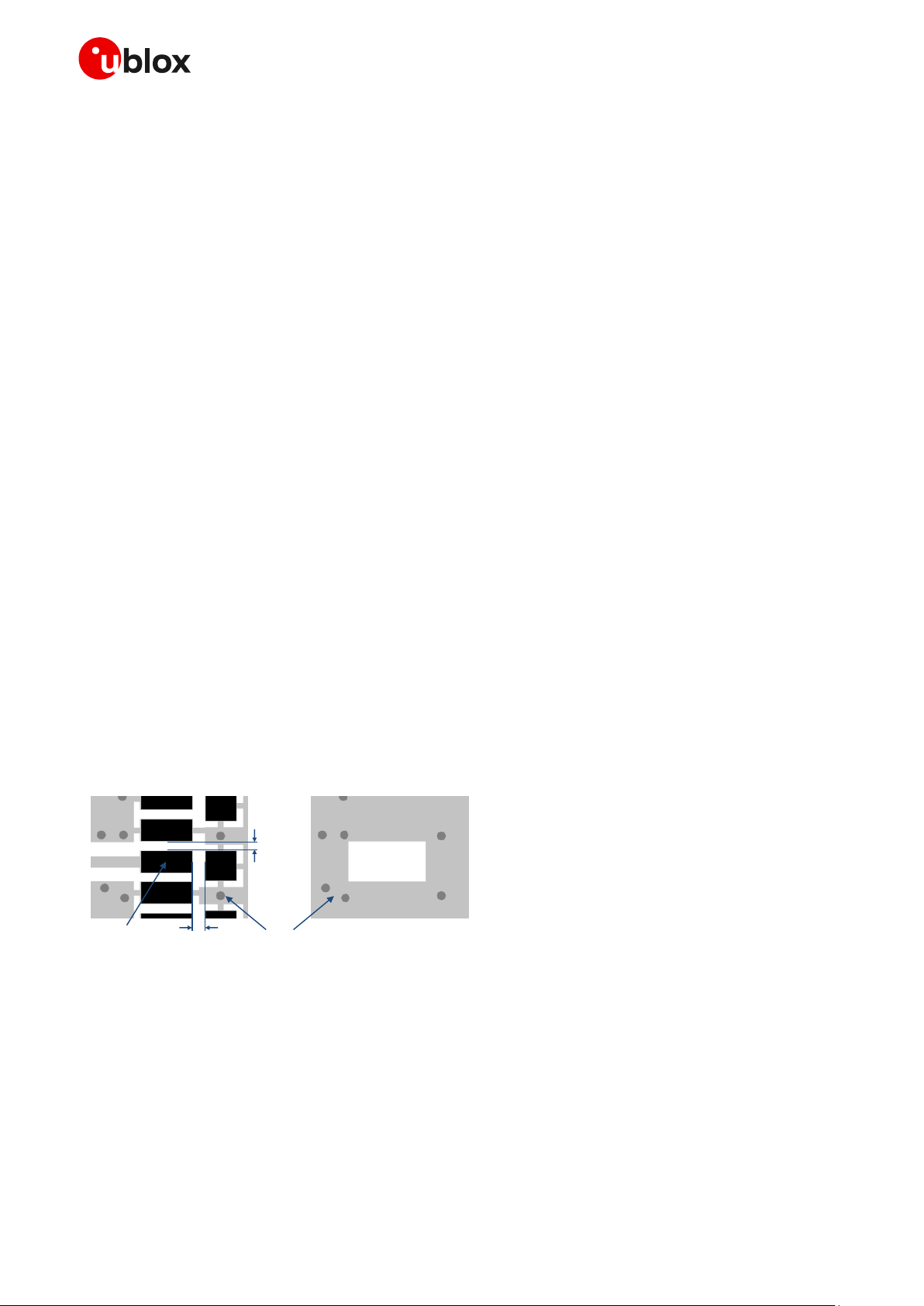
SARA-R4 series - System integration manual
UBX-16029218 - R20 Design-in Page 61 of 128
C1-Public
2.4 Antenna interfaces
SARA-R4 series modules provide an RF interface for connecting the external antenna: the ANT pin
represents the RF input/output for RF signals transmission and reception.
SARA-R422M8S modules provide also a GNSS RF interface for connecting the external GNSS
antenna: the ANT_GNSS pin represents the GNSS RF input for GNSS signals reception.
The ANT and ANT_GNSS pins have a nominal characteristic impedance of 50 and must be
connected to the related external antenna system through a 50 transmission line to allow clean
transmission / reception of RF signals.
2.4.1 General guidelines for antenna interfaces
2.4.1.1 Guidelines for ANT and ANT_GNSS pins RF connection design
☞ The GNSS antenna RF interface is supported by SARA-R422M8S modules only.
A clean transition between the ANT and ANT_GNSS pads and the application board PCB must be
provided, implementing the following design-in guidelines for the layout of the application PCB close
to the ANT and ANT_GNSS pads:
• On a multilayer board, the whole layer stack below the RF connections should be free of digital lines
• Increase GND keep-out (i.e. clearance, a void area) around the ANT and ANT_GNSS pads, on the
top layer of the application PCB, to at least 250 m up to adjacent pads metal definition and up to
400 m on the area below the module, to reduce parasitic capacitance to ground, as described in
the left picture in Figure 35
• Add GND keep-out (i.e. clearance, a void area) on the buried metal layer below the ANT and
ANT_GNSS pads if the top-layer to buried layer dielectric thickness is below 200 m, to reduce
parasitic capacitance to ground, as described in the right picture in Figure 35
Min.
250 µm
Min. 400 µm
GND
RF pad
GND clearance
on buried layer very close to top layer
below RF pad
GND clearance
on top layer
around RF pad
Figure 35: GND keep-out area on top layer around RF pad and on very close buried layer below RF pad (ANT / ANT_GNSS)
Page 62

SARA-R4 series - System integration manual
UBX-16029218 - R20 Design-in Page 62 of 128
C1-Public
2.4.1.2 Guidelines for RF transmission lines design
☞ The GNSS antenna RF interface is supported by SARA-R422M8S modules only.
Any RF transmission line, such as the ones from the ANT and ANT_GNSS pads up to the related
antenna connector or up to the related internal antenna pad, must be designed so that the
characteristic impedance is as close as possible to 50 .
RF transmission lines can be designed as a micro strip (consists of a conducting strip separated from
a ground plane by a dielectric material) or a strip line (consists of a flat strip of metal which is
sandwiched between two parallel ground planes within a dielectric material). The micro strip,
implemented as a coplanar waveguide, is the most common configuration for printed circuit board.
Figure 36 and Figure 37 provide two examples of suitable 50 coplanar waveguide designs. The first
example of RF transmission line can be implemented in case of 4-layer PCB stack-up herein described,
and the second example of RF transmission line can be implemented in case of 2-layer PCB stack-up
herein described.
35 µm
35 µm
35 µm
35 µm
270 µm
270 µm
760 µm
L1 copper
L3 copper
L2 copper
L4 copper
FR-4 dielectric
FR-4 dielectric
FR-4 dielectric
380 µm 500 µm500 µm
Figure 36: Example of 50 coplanar waveguide transmission line design for the described 4-layer board layup
35 µm
35 µm
1510 µm
L2 copper
L1 copper
FR-4 dielectric
1200 µm 400 µm400 µm
Figure 37: Example of 50 coplanar waveguide transmission line design for the described 2-layer board layup
If the two examples do not match the application PCB stack-up, then the 50 characteristic
impedance calculation can be made using the HFSS commercial finite element method solver for
electromagnetic structures from Ansys Corporation, or using freeware tools like Avago / Broadcom
AppCAD (https://www.broadcom.com/appcad) taking care of the approximation formulas used by the
tools for the impedance computation.
To achieve a 50 characteristic impedance, the transmission line width must be chosen due to:
• the thickness of the transmission line itself (e.g. 35 m in the example of Figure 36 and Figure 37)
• the thickness of the dielectric material between the top layer (where the line is routed) and the
inner closer layer implementing the ground plane (e.g. 270 m in Figure 36 and Figure 37)
• the dielectric constant of the dielectric material (e.g. dielectric constant of the FR-4 dielectric
material in Figure 36 and Figure 37)
• the gap from the transmission line to the adjacent ground plane on the same layer of the
transmission line (e.g. 500 m in Figure 36 and 400 m in Figure 37)
Page 63

SARA-R4 series - System integration manual
UBX-16029218 - R20 Design-in Page 63 of 128
C1-Public
If the distance between the transmission line and the adjacent GND area (on the same layer) does not
exceed 5 times the width of the line, use the “Coplanar Waveguide” model for the 50 calculation.
Additionally to the 50 impedance, the following guidelines are recommended for transmission lines:
• Minimize the transmission line length: the insertion loss should be minimized as much as possible,
in the order of a few tenths of a dB,
• Add GND keep-out (i.e. clearance, a void area) on buried metal layers below any pad of component
present on the RF transmission lines, if top-layer to buried layer dielectric thickness is below
200 m, to reduce parasitic capacitance to ground,
• The transmission lines width and spacing to GND must be uniform and routed as smoothly as
possible: avoid abrupt changes of width and spacing to GND,
• Add GND stitching vias around transmission lines, as described in Figure 38,
• Ensure solid metal connection of the adjacent metal layer on the PCB stack-up to main ground
layer, providing enough vias on the adjacent metal layer, as described in Figure 38,
• Route RF transmission lines far from any noise source (as switching supplies and digital lines) and
from any sensitive circuit (as USB),
• Avoid stubs on the transmission lines,
• Avoid signal routing in parallel to transmission lines or crossing the transmission lines on buried
metal layer,
• Do not route microstrip lines below discrete component or other mechanics placed on top layer
Two examples of a suitable RF circuit design for ANT pin are illustrated in Figure 38, where the cellular
antenna detection circuit is not implemented (if the cellular antenna detection function is required by
the application, follow the guidelines for circuit and layout implementation detailed in section 2.4.5):
• In the first example shown on the left, the ANT pin is directly connected to an SMA connector by
means of a suitable 50 transmission line, designed with the appropriate layout.
• In the second example shown on the right, the ANT pin is connected to an SMA connector by means
of a suitable 50 transmission line, designed with the appropriate layout, with an additional high
pass filter to improve the ESD immunity at the antenna port. (The filter consists of a suitable
series capacitor and shunt inductor, for example the Murata GRM1555C1H150JB01 15 pF
capacitor and the Murata LQG15HN39NJ02 39 nH inductor with SRF ~1 GHz.).
SARA module
SMA
connector
SARA module
SMA
connector
High-pass filter
to improve
ESD immunity
Figure 38: Example of circuit and layout for ANT RF circuits on the application board
Page 64

SARA-R4 series - System integration manual
UBX-16029218 - R20 Design-in Page 64 of 128
C1-Public
2.4.1.3 Guidelines for RF termination design
☞ The GNSS antenna RF interface is supported by SARA-R422M8S modules only.
The RF termination must provide a characteristic impedance of 50 as well as the RF transmission
line up to the RF termination, to match the characteristic impedance of ANT and ANT_GNSS ports.
However, real antennas do not have a perfect 50 load on all the supported frequency bands. So to
reduce as much as possible any performance degradation due to antenna mismatching, the RF
termination must provide optimal return loss (or VSWR) figures over all the operating frequencies, as
summarized in Table 7 and Table 8.
If an external antenna is used, the antenna connector represents the RF termination on the PCB:
• Use a suitable 50 connector providing a clean PCB-to-RF-cable transition.
• Strictly follow the connector manufacturer’s recommended layout, for example:
o SMA Pin-Through-Hole connectors require a GND keep-out (i.e. clearance, a void area) on all the
layers around the central pin up to the annular pads of the four GND posts (see Figure 38)
o U.FL surface mounted connectors require no conductive traces (i.e. clearance, a void area) in
the area below the connector between the GND land pads, as illustrated in Figure 39
Figure 39: U.FL surface mounted connector mounting pattern layout
• Cut out the GND layer under the RF connector and close to any buried vias, to remove stray
capacitance and thus keep the RF line at 50 , e.g. the active pad of U.FL connector needs to have
a GND keep-out (i.e. clearance, a void area) at least on the first inner layer to reduce parasitic
capacitance to ground.
If an integrated antenna is used, the integrated antenna represents the RF terminations. The
following guidelines should be followed:
• Use an antenna designed by an antenna manufacturer providing the best possible return loss.
• Provide a ground plane large enough according to the relative integrated antenna requirements.
The ground plane of the application PCB can be reduced down to a minimum size that must be
similar to one quarter of wavelength of the minimum frequency that needs to be radiated. As
numerical example,
Frequency = 617 MHz → Wavelength 48 cm → Minimum GND plane size 12 cm
• It is highly recommended to strictly follow the detailed and specific guidelines provided by the
antenna manufacturer regarding correct installation and deployment of the antenna system,
including the PCB layout and matching circuitry.
• Further to the custom PCB and product restrictions, the antenna may require a tuning to comply
with all the applicable required certification schemes. It is recommended to consult the antenna
manufacturer for antenna matching design-in guidelines relative to the custom application.
Additionally, these recommendations regarding the antenna system placement must be followed:
• Do not place the antennas within a closed metal case.
• Do not place the cellular antenna in close vicinity to the end user since the emitted radiation in
human tissue is restricted by regulatory requirements.
• Place the antennas as far as possible from VCC supply line and related parts (see also Figure 32),
from high speed digital lines (as USB) and from any possible noise source.
Page 65

SARA-R4 series - System integration manual
UBX-16029218 - R20 Design-in Page 65 of 128
C1-Public
• Place the antenna far from sensitive analog systems or employ countermeasures to reduce EMC
or EMI issues.
• Be aware of interaction between co-located RF systems since the LTE transmitted power may
interact or affect the performance of companion systems as a GNSS receiver (see section 2.4.4
for further details and design-in guidelines regarding Cellular / GNSS RF coexistence).
2.4.2 Cellular antenna RF interface (ANT)
2.4.2.1 General guidelines for antenna selection and design
The antenna is the most critical component to be evaluated. Designers must take care of the antenna
from all perspective at the very start of the design phase when the physical dimensions of the
application board are under analysis/decision, since the RF compliance of the device integrating
SARA-R4 series modules with all the applicable required certification schemes depends on antenna’s
radiating performance.
Cellular antennas are typically available as:
• External antennas (e.g. linear monopole):
o External antennas basically do not imply physical restriction to the design of the PCB where
the SARA-R4 series module is mounted.
o The radiation performance mainly depends on the antennas. It is required to select antennas
with optimal radiating performance in the operating bands.
o RF cables should be carefully selected to have minimum insertion losses. Additional insertion
loss will be introduced by low quality or long cable. Large insertion loss reduces both transmit
and receive radiation performance.
o A high quality 50 RF connector provides a clean PCB-to-RF-cable transition. It is
recommended to strictly follow the layout and cable termination guidelines provided by the
connector manufacturer.
• Integrated antennas (e.g. PCB antennas such as patches or ceramic SMT elements):
o Internal integrated antennas imply physical restriction to the design of the PCB: Integrated
antenna excites RF currents on its counterpoise, typically the PCB ground plane of the device
that becomes part of the antenna: its dimension defines the minimum frequency that can be
radiated. Therefore, the ground plane can be reduced down to a minimum size that should be
similar to the quarter of the wavelength of the minimum frequency that needs to be radiated,
given that the orientation of the ground plane relative to the antenna element must be
considered. As numerical example, the physical restriction to the PCB design can be
considered as following:
Frequency = 750 MHz → Wavelength = 40 cm → Minimum GND plane size = 10 cm
o Radiation performance depends on the whole PCB and antenna system design, including
product mechanical design and usage. Antennas should be selected with optimal radiating
performance in the operating bands according to the mechanical specifications of the PCB and
the whole product.
o It is recommended to select a custom antenna designed by an antennas’ manufacturer if the
required ground plane dimensions are very small (e.g. less than 6.5 cm long and 4 cm wide).
The antenna design process should begin at the start of the whole product design process
o It is highly recommended to strictly follow the detailed and specific guidelines provided by the
antenna manufacturer regarding correct installation and deployment of the antenna system,
including PCB layout and matching circuitry
o Further to the custom PCB and product restrictions, antennas may require tuning to obtain
the required performance for compliance with all the applicable required certification schemes.
It is recommended to consult the antenna manufacturer for the design-in guidelines for
antenna matching relative to the custom application
Page 66

SARA-R4 series - System integration manual
UBX-16029218 - R20 Design-in Page 66 of 128
C1-Public
In both of cases, selecting external or internal antennas, these recommendations should be observed:
• Select an antenna providing optimal return loss / VSWR / efficiency figure over all the operating
cellular frequencies.
• Select an antenna providing the worst possible return loss / VSWR / efficiency figure in the GNSS
frequency band, to optimize the RF coexistence between the cellular and the GNSS systems (see
section 2.4.4 for further details and guidelines regarding Cellular / GNSS RF coexistence).
• Select an antenna providing appropriate gain figure (i.e. combined antenna directivity and
efficiency figure) so that the electromagnetic field radiation intensity do not exceed the regulatory
limits specified in some countries, such as FCC United States (see section 4.2.2), ISED Canada
(see section 4.3.1), RED Europe (see section 4.4), GITEKI Japan (see section 4.8), etc.
2.4.2.2 Examples of cellular antennas
Table 23 lists some examples of possible internal on-board surface-mount antennas.
Manufacturer
Part number
Product name
Description
Taoglas
PA.710.A
Warrior
GSM / WCDMA / LTE SMD antenna
698..960 MHz, 1710..2170 MHz, 2300..2400 MHz, 2490..2690 MHz
40.0 x 6.0 x 5.0 mm
Taoglas
PCS.26.A
Havok
LTE SMD dielectric antenna
617..960 MHz, 1710..2690 MHz
54.6 x 13.0 x 3.0 mm
Taoglas
PCS.66.A
Reach
Wideband LTE SMD antenna
600..6000 MHz
32.0 x 25.0 x 1.6 mm
Antenova
SR4L002
Lucida
GSM / WCDMA / LTE SMD antenna
698..960 MHz, 1710..2170 MHz, 2300..2400 MHz, 2490..2690 MHz
35.0 x 8.5 x 3.2 mm
Ethertronics
P822601
GSM / WCDMA / LTE SMD antenna
698..960 MHz, 1710..2170 MHz, 2490..2700 MHz
50.0 x 8.0 x 3.2 mm
Ethertronics
P822602
GSM / WCDMA / LTE SMD antenna
698..960 MHz, 1710..2170 MHz, 2490..2700 MHz
50.0 x 8.0 x 3.2 mm
Ethertronics
1002436
GSM / WCDMA / LTE vertical mount antenna
698..960 MHz, 1710..2700 MHz
50.6 x 19.6 x 1.6 mm
Fractus
NN03-310
TRIO mXTEND™
GSM / WCDMA / LTE SMD antenna
698..8000 MHz
30.0 x 3.0 x 1.0 mm
Pulse
W3796
Domino
GSM / WCDMA / LTE SMD antenna
698..960 MHz, 1427..1661 MHz, 1695..2200 MHz, 2300..2700 MHz
42.0 x 10.0 x 3.0 mm
TE Connectivity
2118310-1
GSM / WCDMA / LTE vertical mount antenna
698..960 MHz, 1710..2170 MHz, 2300..2700 MHz
74.0 x 10.6 x 1.6 mm
Molex
1462000001
GSM / WCDMA / LTE SMD antenna
698..960 MHz, 1700..2700 MHz
40.0 x 5.0 x 5.0 mm
Cirocomm
DSAN0001
Ceramic LTE SMD antenna
698..960 MHz, 1710..2170 MHz
40.0 x 6.0 x 5.0 mm
Table 23: Examples of internal surface-mount antennas
Page 67

SARA-R4 series - System integration manual
UBX-16029218 - R20 Design-in Page 67 of 128
C1-Public
Table 24 lists some examples of possible internal off-board PCB-type antennas with cable and
connector.
Manufacturer
Part number
Product name
Description
PulseLarsen
Antennas
W3929B0100
LTE FPC antenna with coax feed
617..960 MHz, 1710..2690 MHz, 3400..3900 MHz
115.8 x 30.4 mm
Taoglas
FXUB64.18.0150A
Cyclone
LTE wideband flex antenna
617..960 MHz, 1710..2690 MHz
130.0 x 30.0 mm
Taoglas
FXUB63.07.0150C
GSM / WCDMA / LTE PCB antenna with cable and U.FL
698..960 MHz, 1575.42 MHz, 1710..2170 MHz, 2400..2690 MHz
96.0 x 21.0 mm
Laird Tech.
EFF692SA3S
Revie Flex
Flexible LTE antenna
689..875 MHz, 1710..2500 MHz
90.0 x 20.0 mm
Antenova
SRFL026
Mitis
GSM / WCDMA / LTE antenna on flexible PCB with cable and U.FL
689..960 MHz, 1710..2170 MHz, 2300..2400 MHz, 2500..2690 MHz
110.0 x 20.0 mm
Ethertronics
1002289
GSM / WCDMA / LTE antenna on flexible PCB with cable and U.FL
698..960 MHz, 1710..2700 MHz
140.0 x 75.0 mm
EAD
FSQS35241-UF-10
SQ7
GSM / WCDMA / LTE PCB antenna with cable and U.FL
690..960 MHz, 1710..2170 MHz, 2500..2700 MHz
110.0 x 21.0 mm
Table 24: Examples of internal antennas with cable and connector
Table 25 lists some examples of possible external antennas.
Manufacturer
Part number
Product name
Description
Taoglas
GSA.8842.A.105111
Wideband LTE I-Bar adhesive antenna with cable and SMA(M)
617..960 MHz, 1710..2700 MHz, 4900..5850 MHz
176.5 x 59.2 x 13.6 mm
Taoglas
TG.55.8113
LTE terminal mount monopole antenna with 90° hinged SMA(M)
617..960 MHz, 1427..2170 MHz, 2300..2690 MHz
172.0 x 23.88 x 13 mm
Taoglas
TG.35.8113W
Apex II
Wideband LTE dipole terminal antenna hinged SMA(M)
617..1200 MHz, 1710..2700 MHz, 4900..5900 MHz
224 x 58 x 13 mm
Laird Tech.
TRA6927M3PW-001
GSM / WCDMA / LTE screw-mount antenna with N-type(F)
698..960 MHz, 1710..2170 MHz, 2300..2700 MHz
83.8 x Ø 36.5 mm
Laird Tech.
CMS69273
GSM / WCDMA / LTE ceiling-mount antenna with cable and N-type(F)
698..960 MHz, 1575.42 MHz, 1710..2700 MHz
86 x Ø 199 mm
Laird Tech.
OC69271-FNM
GSM / WCDMA / LTE pole-mount antenna with N-type(M)
698..960 MHz, 1710..2690 MHz
248 x Ø 24.5 mm
Pulse
Electronics
SPDA24617/3900
Multiband swivel dipole antenna with SMA(M)
617..960 MHz, 1400..2700 MHz, 3200..3900 MHz
223.24 x 56.13 x 10.97 mm
Table 25: Examples of external antennas
Page 68

SARA-R4 series - System integration manual
UBX-16029218 - R20 Design-in Page 68 of 128
C1-Public
2.4.3 GNSS antenna RF interface (ANT_GNSS)
☞ The GNSS antenna RF interface is supported by SARA-R422M8S modules only.
☞ For additional information and guidelines regarding the GNSS design, see the u-blox SARA-R4 /
SARA-R5 positioning implementation application note [21].
The antenna and its placement are critical system factors for accurate GNSS reception. Use of a
ground plane will minimize the effects of ground reflections and enhance the antenna efficiency. A
good allowance for ground plane size is typically in the area of 50 x 50 to 70 x 70 mm2. The smaller the
electrical size of the plane, the narrower the reachable bandwidth and the lower the radiation
efficiency. Exercise care with rover vehicles that emit RF energy from motors etc. as interference may
extend into the GNSS band and couple into the GNSS antenna suppressing the wanted signal. For
more details about GNSS antennas, see also the u-blox GNSS antennas application note [22].
Since SARA-R422M8S modules already include an internal SAW filter followed by an additional LNA
before the u-blox M8 GNSS chipset (as illustrated in Figure 4), they are optimized to work with passive
or active antennas without requiring additional external circuitry.
2.4.3.1 Guidelines for applications with a passive antenna
If a GNSS passive antenna with high gain and good sky view is used, together with a short 50 line
between antenna and receiver, and no jamming sources affect the GNSS passive antenna, the circuit
illustrated in Figure 40 can be used. This provides the minimum BoM cost and minimum board space.
SARA-R422M8S
31
ANT_GNSS
GND
Figure 40: Minimum circuit with GNSS passive antenna
If the connection between the module and antenna incurs additional losses (e.g. antenna placed far
away from the module, small ground plane for a patch antenna) or improved jamming immunity is
needed due to strong out-of-band jammers close to the GNSS antenna (e.g. the cellular antenna is
close to the GNSS antenna), consider adding an external SAW filter (see Table 26 for possible suitable
examples) close to the GNSS passive antenna, followed by an external LNA (see Table 27 for possible
suitable examples), as illustrated in Figure 41, provided that SARA-R422M8S modules already include
dedicated internal SAW filter followed by an LNA before the u-blox M8 GNSS chipset (as illustrated in
Figure 4), so that additional external SAW and LNA are not required for most of the applications (see
section 2.4.4 for further details and design-in guidelines regarding Cellular / GNSS RF coexistence).
☞ An external LNA with related external SAW filter are only required if the GNSS antenna is far away
(more than 10 cm) from the GNSS RF input of the module. In that case, the SAW and the LNA
must be placed close to the passive antenna.
Page 69

SARA-R4 series - System integration manual
UBX-16029218 - R20 Design-in Page 69 of 128
C1-Public
SARA-R422M8S
31
ANT_GNSS
GND
SAW LNA
44
ANT_ON
Figure 41: Typical circuit for best performance and improved jamming immunity with GNSS passive antenna
The external LNA can be selected to deliver the performance needed by the application in terms of:
• Noise figure (sensitivity)
• Selectivity and linearity (robustness against jamming)
• Robustness against RF power
Depending on the characteristics of the supply source (DC/DC regulator, linear LDO regulator or other)
used to supply the external LNA, make sure some good filtering is in place for the external LNA supply
because of the noise on the external LNA supply line can affect the performance of the LNA itself:
consider adding a proper series ferrite bead (see Table 28 for possible suitable examples) and a proper
decoupling capacitor to ground with Self-Resonant Frequency in the GNSS frequency range (as for
example the 27 pF 0402 capacitor Murata GCM1555C1H270JA16) at the input of the external LNA
supply line.
It should be noted anyway that the insertion loss of the filter directly affects the system noise figure
and hence the system performance. The selected SAW filter has to provide very low loss (no more
than 1.5 dB) in the GNSS pass-band, beside providing very large attenuation (more than 40 to 60 dB)
in the out-of-band jammers’ cellular frequency bands (see Table 26 for possible suitable examples).
SARA-R422M8S already provides an integrated SAW filter and LNA (as illustrated in Figure 4). The
addition of such external components should be carefully evaluated, especially in case the application
power consumption should be minimized, since the LNA alone requires an additional supply current
of typically 5 to 20 mA.
Moreover, the first LNA of the input chain will dominate the receiver noise performance, therefore its
noise figure should be less than 2 dB. If the antenna is close to the receiver, then a good passive
antenna (see Table 29) can be directly connected to the receiver with a short (a few cm) 50 line.
From a noise point of view, this design choice offers comparable performance as an active antenna
with a long (~3 to 5m) cable attached to the application board by means of an SMA connector without
the increased power consumption and BOM cost. If the goal is to protect the GNSS receiver in a noisy
environment then an additional external SAW filter may be required. If a degradation in the C/No of 2
to 3 dB (depending on the choice of the filter) is not acceptable for the application, then, to
compensate for the filter losses and restore an adequate C/No level, an external LNA with good gain
and low noise figure (see Table 27) is to be considered.
Table 26 lists examples of SAW filters suitable for the GNSS RF input of SARA-R422M8S modules.
Manufacturer
Part number
Description
Murata
SAFFB1G56AC0F0A
GPS / SBAS / QZSS / GLONASS / Galileo / BeiDou RF band-pass SAW
filter with high attenuation in Cellular frequency ranges
Murata
SAFFB1G56AC0F7F
GPS / SBAS / QZSS / GLONASS / Galileo / BeiDou RF band-pass SAW
filter with high attenuation in Cellular frequency ranges
Table 26: Examples of GNSS band-pass SAW filters
Page 70

SARA-R4 series - System integration manual
UBX-16029218 - R20 Design-in Page 70 of 128
C1-Public
Table 27 lists examples of LNA suitable for the GNSS RF input of SARA-R422M8S modules.
Manufacturer
Part number
Comments
Maxim
MAX2659ELT+
Low noise figure, up to 10 dBm RF input power
JRC New Japan Radio
NJG1143UA2
Low noise figure, up to 15 dBm RF input power
NXP
BGU8006
Low noise figure, very small package size (WL-CSP)
Infineon
BGA524N6
Low noise figure, small package size
Table 27: Examples of GNSS Low Noise Amplifiers
Table 28 lists examples of ferrite beads suitable for the supply line of an external GNSS LNA.
Manufacturer
Part number
Comments
Murata
BLM15HD102SN1
High impedance at 1.575 GHz
Murata
BLM15HD182SN1
High impedance at 1.575 GHz
TDK
MMZ1005F121E
High impedance at 1.575 GHz
TDK
MMZ1005A121E
High impedance at 1.575 GHz
Table 28: Examples of ferrite beads for the supply line of external GNSS Low Noise Amplifiers
Table 29 lists examples of passive antennas suitable for the GNSS RF input of SARA-R422M8S.
Manufacturer
Part number
Product name
Description
Tallysman
TW3400P
Passive antenna
GPS / SBAS / QZSS / GLONASS
Tallysman
TW3710P
Passive antenna
GPS / SBAS / QZSS / GLONASS / Galileo / BeiDou
Taoglas
CGGBP.35.3.A.02
Ceramic patch antenna
GPS / SBAS / QZSS / GLONASS / Galileo / BeiDou
Taoglas
CGGBP.18.4.A.02
Embedded patch antenna
GPS / SBAS / QZSS / GLONASS / Galileo / BeiDou
Inpaq
PA1590MF6G
Patch antenna
GPS / SBAS / QZSS / GLONASS
Yageo
ANT2525B00BT1516S
Ceramic patch antenna
GPS / SBAS / QZSS / GLONASS
Antenova
SR4G008
Sinica
Ultra-low profile patch antenna
GPS / SBAS / QZSS / GLONASS / Galileo / BeiDou
Table 29: Examples of GNSS passive antennas
2.4.3.2 Guidelines for applications with an active antenna
Active antennas offer higher gain and better overall performance compared with passive antennas
(without additional external SAW filter and LNA). However, the integrated low-noise amplifier
contributes an additional current of typically 5 to 20 mA to the ’ystem's power consumption budget.
Active antennas for GNSS applications are usually powered through a DC bias on the RF cable. A
simple bias-T, as shown in Figure 42, can be used to add this DC current to the RF signal line. The
inductance L is responsible for isolating the RF path from the DC path. It should be selected to offer
high impedance (> 500 Ω) at L-band frequencies. A series current limiting resistor is required to
prevent short circuits destroying the bias-t inductor.
Page 71

SARA-R4 series - System integration manual
UBX-16029218 - R20 Design-in Page 71 of 128
C1-Public
To avoid damaging the bias-T series inductor in the case of a short circuit at the antenna connector,
it is recommended to implement a proper over-current protection circuit, which may consist in a series
resistor as in the example illustrated in Figure 42. Component values are calculated according to the
characteristics of the active antenna and the related supply circuit in use: the value of R
bias
is
calculated such that the maximum current capacity of the inductor L is never exceeded. Moreover,
R
bias
and C form a low pass filter to remove high frequency noise from the DC supply. Assuming
VCC_ANT=3.3 V, Table 30 reports suggested components for the circuit in Figure 42.
The recommended bias-t inductor (Murata LQW15ANR12J00) has a maximum current capacity of
110 mA. Hence the current is limited to 100 mA by way of a 33 ohm bias resistor. This resistor power
rating must be chosen to ensure reliability in the chosen circuit design.
SARA-R422M8S
31
ANT_GNSS
GND
LNA
Active antenna
Coaxial antenna
cable
VCC_ANT
Rbias
C
L
44
44
ANT_ON
ESD
Figure 42: Typical circuit with active antenna connected to GNSS RF interface of SARA-R422M8S, using an external supply
Reference
Description
Part number - Manufacturer
L
120 nH wire-wound RF Inductor 0402 5% 110 mA
LQW15ANR12J00 - Murata
C
100 nF capacitor ceramic X7R 0402 10% 16 V
GCM155R71C104KA55 - Murata
Rbias
33 ohm resistor 0.5W
Various manufacturers
Table 30: Example component values for active antenna biasing
☞ Refer to the antenna datasheet and/or manufacturer for proper values of the supply voltage
VCC_ANT, inductance L and capacitance C.
☞ ESD sensitivity rating of the ANT_GNSS RF input pin is 1 kV (HBM according to JESD22-A114).
Higher protection level can be required if the line is externally accessible on the application board.
Higher protection level can be achieved by mounting an ultra low capacitance (i.e. < 1 pF) ESD
protection (see Table 31) close to accessible point.
Table 31 lists examples of ESD protection suitable for the GNSS RF input of SARA-R422M8S.
Manufacturer
Part number
Description
ON Semiconductor
ESD9R3.3ST5G
ESD protection diode with ultra−low capacitance (0.5 pF)
Infineon
ESD5V3U1U-02LS
ESD protection diode with ultra−low capacitance (0.4 pF)
Littelfuse
PESD0402-140
ESD protection diode with ultra−low capacitance (0.25 pF)
Table 31: Examples of ultra−low capacitance ESD protections
Page 72

SARA-R4 series - System integration manual
UBX-16029218 - R20 Design-in Page 72 of 128
C1-Public
Table 32 lists examples of active antennas to be used with SARA-R422M8S modules.
Manufacturer
Part number
Product name
Description
Tallysman
TW3400
Active antenna– 2.5 - 16 V
GPS / SBAS / QZSS / GLONASS
Tallysman
TW3710
Active antenna, 2.5 – 16 V
GPS / SBAS / QZSS / GLONASS / Galileo / BeiDou
Taoglas
AA.162.301111
Ulysses
Ultra-Low profile miniature antenna, 1.8 – 5.5V
GPS / SBAS / QZSS / GLONASS / Galileo
Taoglas
MA310.A.LB.001
Magnet mount antenna, 1.8 – 5.5 V
GPS / SBAS / QZSS / GLONASS
Inpaq
B3G02G-S3-01-A
SMA plug active antenna, 3.3 V typical
GPS / SBAS / GLONASS
Inpaq
GPSH237N-N3-37-A
Patch circular antenna, 3.0 V typical
GPS / SBAS / QZSS
Abracon LLC
APAMP-110
Module RF antenna 5dBic SMA adhesive, 2.5 – 3.5 V
GPS / SBAS / QZSS
TE Connectivity
2195768-1
Active antenna, 3.0 V typical
GPS / SBAS / QZSS
Table 32: Examples of GNSS active antennas
2.4.4 Cellular and GNSS RF coexistence
Overview
Desensitization or receiver blocking is a form of electromagnetic interference where a radio receiver
is unable to detect a weak signal that it might otherwise be able to receive when there is no
interference (see Figure 43). Good blocking performance is particularly important in the scenarios
where a number of radios of various forms are used in close proximity to each other.
0
-120
-60
1575
Frequency [MHz]
Power [dBm]
Filter gain [dB]
1800
2025
1350
1125
GNSS signal
LTE signal
Filter response
Figure 43: Interference due to transmission in LTE B3, B4 and B66 low channels (1710 MHz) adjacent to GNSS frequency
range (1561 to 1605 MHz). Harmonics due to transmission in LTE B13 high channels (787 MHz) may fall into the GNSS bands
Jamming signals may come from in-band and out-of-band frequency sources. In-band jamming is
caused by signals with frequencies falling within the GNSS frequency range, while the out-of-band
jamming is caused by very strong signals adjacent to the GNSS frequency range so that part of the
strong signal power may leak at the input of the GNSS receiver and/or block GNSS reception.
If not properly taken into consideration, in-band and out-band jamming signals may cause a reduction
in the carrier-to-noise power density ratio (C/No) of the GNSS satellites.
Page 73

SARA-R4 series - System integration manual
UBX-16029218 - R20 Design-in Page 73 of 128
C1-Public
In-band interference
In-band interference signals are typically caused by harmonics from displays, switching converters,
micro-controllers and bus systems. Moreover, considering for example the LTE band 13 high channel
transmission frequency (787 MHz) and the GPS operating band (1575.42 MHz ± 1.023 MHz), the
second harmonic of the cellular signal is exactly within the GPS operating band. Therefore, depending
on the board layout and the transmit power, the highest channel of LTE band 13 is the channel that
has the greatest impact on the C/No reduction.
Countermeasures against in-band interference include:
• maintaining a good grounding concept in the design
• ensuring proper shielding of the different RF paths
• ensuring proper impedance matching of RF traces
• placing the GNSS antenna away from noise sources
• add a notch filter along the GNSS RF path, just after the antenna, at the frequency of the jammer
(as for example illustrated in Figure 44)
SARA-R422M8S
31 ANT_GNSS
L1
GND
C1
Figure 44: Simple notch filter for improved in-band jamming immunity against a single jamming frequency
With reference to Figure 44, a simple notch filter can be realized by the series connection of an
inductor and capacitor. Capacitor C1 and inductor L1 values are calculated according to the formula:
𝑓 =
1
2 𝜋 √𝐶 ⋅ 𝐿
For example, a notch filter at ~787 MHz improves the GNSS immunity to LTE band 13 high channel.
Suitable component nominal values are C1 = 3.3 pF and L1 = 12 nH, with tolerance less than or equal
to 2 % to ensure adequate notch frequency accuracy.
Out-of-band interference
Out-of-band interference is caused by signal frequencies that are different from the GNSS, the main
sources being cellular, Wi-Fi, bluetooth transmitters, etc. For example, the lowest channels in LTE
band 3, 4 and 66 can compromise the good reception of the GLONASS satellites. Again, the effect can
be explained by comparing the LTE frequencies (low channel transmission frequency is 1710 MHz)
with the GLONASS operating band (1602 MHz ± 8 MHz). In this case the LTE signal is outside the
useful GNSS band, but provided that the power received by the GNSS subsystem at 1710 MHz is high
enough, blocking and leakage effects may appear reducing once again the C/No.
Countermeasures against out-of-band interference include:
• maintaining a good grounding concept in the design
• keeping the GNSS and cellular antennas more than the quarter-wavelength (of the minimum Tx
frequency) away from each other. If for layout or size reasons this requirement cannot be met,
then the antennas should be placed orthogonally to each other and/or on different side of the PCB.
Page 74

SARA-R4 series - System integration manual
UBX-16029218 - R20 Design-in Page 74 of 128
C1-Public
• selecting a cellular antenna providing the worst possible return loss / VSWR / efficiency figure in
the GNSS frequency band: the lower is the cellular antenna efficiency between 1575 MHz and
1610 MHz, the higher is the isolation between the cellular and the GNSS systems
• ensuring at least 15 – 20 dB isolation between antennas in the GNSS band by implementing the
most suitable placement for the antennas, considering in particular the related radiation diagrams
of the antennas: better isolation results from antenna patterns with radiation lobes in different
directions considering the GNSS frequency band.
• adding a GNSS pass-band SAW filter along the GNSS RF line, providing very large attenuation in
the cellular frequency bands (see Table 26 for possible suitable examples). It has to be noted that,
as shown in Figure 4, a SAW filter and an LNA are already integrated in the GNSS RF path of the
SARA-R422M8S: the addition of an external filter along the GNSS RF line has to be considered
only if the conditions above cannot be met.
Additional countermeasures
In case all the aforementioned countermeasures cannot be implemented, adding a GNSS stop-band
SAW filter along the cellular RF line may be considered. The filter shall provide very low attenuation in
the cellular frequency bands (see Table 33 for possible suitable examples). It has to be noted that the
addition of an external filter along the cellular RF line has to be carefully evaluated, considering that
the additional insertion loss of such filter may affect the cellular TRP and/or TIS RF figures.
Table 33 lists examples of GNSS band-stop SAW filters that may be considered for the cellular RF
input/output in case enough isolation between the cellular and the GNSS RF systems cannot be
provided by proper selection and placement of the antennas beside other proper RF design solutions.
Manufacturer
Part number
Description
Qualcomm
B8636
GPS / SBAS / QZSS / GLONASS / Galileo / BeiDou RF band-stop SAW
filter with low attenuation in Cellular frequency ranges
Qualcomm
B8666
GPS / SBAS / QZSS / GLONASS / Galileo / BeiDou RF band-stop SAW
filter with low attenuation in Cellular frequency ranges
Table 33: Examples of GNSS band-stop SAW filters
Additional considerations
As far as the RF Tx power is involved in the cellular / GNSS RF coexistence, it has to be noted that
high-power transmission occurs very infrequently: typical values are in the range of -3 to 0 dBm (see
Figure 1 in the GSMA official document TS.09 [12]). Therefore, depending on the application, careful
PCB layout, antenna selection and placement should be sufficient to ensure accurate GNSS reception.
For an example of vehicle tracking application in a small form factor featuring cellular and short-range
connectivity alongside a multi-constellation GNSS receiver, with successful RF coexistence between
the systems, refer to the u-blox B36 vehicle tracking blueprint [23]. The distance between the cellular
and GNSS antennas for the u-blox B36 blueprint is annotated in Figure 45.
GNSS
antenna
5.5 cm
Cellular
antenna
SARA
module
Figure 45: PCB top rendering for the u-blox B36 blueprint with annotated distance between cellular and GNSS antennas
Page 75

SARA-R4 series - System integration manual
UBX-16029218 - R20 Design-in Page 75 of 128
C1-Public
2.4.5 Antenna detection interface (ANT_DET)
2.4.5.1 Guidelines for ANT_DET circuit design
Figure 46 and Table 34 describe the recommended schematic / components for the antenna
detection circuit that must be provided on the application board and for the diagnostic circuit that
must be provided on the antenna’s assembly to achieve antenna detection functionality.
Application Board
Antenna Cable
SARA-R4 series
56
ANT
62
ANT_DET
R1
C1 D1
L1
C2
J1
Z0= 50
Ω
Z0= 50
Ω
Z0= 50 ohm
Antenna Assembly
R2
C4
L3
Radiating
Element
Diagnostic
Circuit
GND
L2
C3
Figure 46: Suggested schematic for antenna detection circuit on application PCB and diagnostic circuit on antenna assembly
Reference
Description
Part Number - Manufacturer
C1
27 pF Capacitor Ceramic C0G 0402 5% 50 V
GRM1555C1H270J - Murata
C2
33 pF Capacitor Ceramic C0G 0402 5% 50 V
GRM1555C1H330J - Murata
D1
Very Low Capacitance ESD Protection
PESD0402-140 - Tyco Electronics
L1
68 nH Multilayer Inductor 0402 (SRF ~1 GHz)
LQG15HS68NJ02 - Murata
R1
10 k Resistor 0402 1% 0.063 W
RK73H1ETTP1002F - KOA Speer
J1
SMA Connector 50 Through Hole Jack
SMA6251A1-3GT50G-50 - Amphenol
C3
15 pF Capacitor Ceramic C0G 0402 5% 50 V
GRM1555C1H150J - Murata
L2
39 nH Multilayer Inductor 0402 (SRF ~1 GHz)
LQG15HN39NJ02 - Murata
C4
22 pF Capacitor Ceramic C0G 0402 5% 25 V
GRM1555C1H220J - Murata
L3
68 nH Multilayer Inductor 0402 (SRF ~1 GHz)
LQG15HS68NJ02 - Murata
R2
15 k Resistor for Diagnostics
Various Manufacturers
Table 34: Suggested parts for antenna detection circuit on application PCB and diagnostic circuit on antennas assembly
The antenna detection circuit and diagnostic circuit suggested in Figure 46 and Table 34 are here
explained:
• When antenna detection is forced by the +UANTR AT command, the ANT_DET pin generates a DC
current measuring the resistance (R2) from the antenna connector (J1) provided on the
application board to GND.
• DC blocking capacitors are needed at the ANT pin (C2) and at the antenna radiating element (C4)
to decouple the DC current generated by the ANT_DET pin.
• Choke inductors with a Self-Resonance Frequency (SRF) in the range of 1 GHz are needed in series
at the ANT_DET pin (L1) and in series at the diagnostic resistor (L3), to avoid a reduction of the
RF performance of the system, improving the RF isolation of the load resistor.
• Resistor on the ANT_DET path (R1) is needed for accurate measurements through the +UANTR
AT command. It also acts as an ESD protection.
• Additional components (C1 and D1 in Figure 46) are provided as ANT_DET pin as ESD protection.
• Additional high pass filter (C3 and L2 in Figure 46) is provided as ESD immunity improvement
• The ANT pin must be connected to the antenna connector by means of a transmission line with
nominal characteristics impedance as close as possible to 50 .
Page 76

SARA-R4 series - System integration manual
UBX-16029218 - R20 Design-in Page 76 of 128
C1-Public
The DC impedance at RF port for some antennas may be a DC open (e.g. linear monopole) or a DC short
to reference GND (e.g. PIFA antenna). For those antennas, without the diagnostic circuit of Figure 46,
the measured DC resistance is always at the limits of the measurement range (respectively open or
short), and there is no mean to distinguish between a defect on antenna path with similar
characteristics (respectively: removal of linear antenna or RF cable shorted to GND for PIFA antenna).
Furthermore, any other DC signal injected to the RF connection from ANT connector to radiating
element will alter the measurement and produce invalid results for antenna detection.
☞ It is recommended to use an antenna with a built-in diagnostic resistor in the range from 5 k to
30 k to assure good antenna detection functionality and avoid a reduction of module RF
performance. The choke inductor should exhibit a parallel Self Resonance Frequency (SRF) in the
range of 1 GHz to improve the RF isolation of load resistor.
For example:
Consider an antenna with built-in DC load resistor of 15 k. Using the +UANTR AT command, the
module reports the resistance value evaluated from the antenna connector provided on the
application board to GND:
• Reported values close to the used diagnostic resistor nominal value (i.e. values from 13 k to 17
k if a 15 k diagnostic resistor is used) indicate that the antenna is correctly connected.
• Values close to the measurement range maximum limit (approximately 50 k) or an open-circuit
“over range” report (see the SARA-R4 series AT commands manual [2]) means that that the
antenna is not connected or the RF cable is broken.
• Reported values below the measurement range minimum limit (1 k) highlights a short to GND at
antenna or along the RF cable.
• Measurement inside the valid measurement range and outside the expected range may indicate
an unclean connection, a damaged antenna or incorrect value of the antenna load resistor for
diagnostics.
• Reported value could differ from the real resistance value of the diagnostic resistor mounted
inside the antenna assembly due to antenna cable length, antenna cable capacity and the used
measurement method.
☞ If the antenna detection function is not required by the customer application, the ANT_DET pin
can be left not connected and the ANT pin can be directly connected to the antenna connector by
means of a 50 transmission line as described in Figure 38.
Page 77

SARA-R4 series - System integration manual
UBX-16029218 - R20 Design-in Page 77 of 128
C1-Public
2.4.5.2 Guidelines for ANT_DET layout design
Figure 47 describes the recommended layout for the antenna detection circuit to be provided on the
application board to achieve antenna detection functionality, implementing the recommended
schematic described in the previous Figure 46 and Table 34:
• The ANT pin must be connected to the antenna connector by means of a 50 transmission line,
implementing the design guidelines described in section 2.4.2 and the recommendations of the
SMA connector manufacturer.
• DC blocking capacitor at ANT pin (C2) must be placed in series to the 50 RF line.
• The ANT_DET pin must be connected to the 50 transmission line by means of a sense line.
• Choke inductor in series at the ANT_DET pin (L1) must be placed so that one pad is on the 50
transmission line and the other pad represents the start of the sense line to the ANT_DET pin.
• The additional components (R1, C1 and D1) are provided as ANT_DET ESD protection.
• The additional high pass filter (C3 and L2) is provided as ESD immunity improvement.
SARA module
C2
R1
D1
C1
L1
J1
C3 L2
Figure 47: Suggested layout for antenna detection circuit on application board
Page 78

SARA-R4 series - System integration manual
UBX-16029218 - R20 Design-in Page 78 of 128
C1-Public
2.5 SIM interface
2.5.1 Guidelines for SIM circuit design
2.5.1.1 Guidelines for SIM cards, SIM connectors and SIM chips selection
The ISO/IEC 7816, the ETSI TS 102 221 and the ETSI TS 102 671 specifications define the physical,
electrical and functional characteristics of Universal Integrated Circuit Cards (UICC), which contains
the Subscriber Identification Module (SIM) integrated circuit that securely stores all the information
needed to identify and authenticate subscribers over the LTE network.
Removable UICC / SIM card contacts mapping is defined by ISO/IEC 7816 and ETSI TS 102 221 as
follows:
• Contact C1 = VCC (Supply) → It must be connected to VSIM
• Contact C2 = RST (Reset) → It must be connected to SIM_RST
• Contact C3 = CLK (Clock) → It must be connected to SIM_CLK
• Contact C4 = AUX1 (Auxiliary contact) → It must be left not connected
• Contact C5 = GND (Ground) → It must be connected to GND
• Contact C6 = VPP/SWP (Other function) → It can be left not connected
• Contact C7 = I/O (Data input/output) → It must be connected to SIM_IO
• Contact C8 = AUX2 (Auxiliary contact) → It must be left not connected
A removable SIM card can have 6 contacts (C1, C2, C3, C5, C6, C7) or 8 contacts, also including the
auxiliary contacts C4 and C8. Only 6 contacts are required and must be connected to the module SIM
interface.
Removable SIM cards are suitable for applications requiring a change of SIM card during the product
lifetime.
A SIM card holder can have 6 or 8 positions if a mechanical card presence detector is not provided, or
it can have 6+2 or 8+2 positions if two additional pins relative to the normally-open mechanical switch
integrated in the SIM connector for the mechanical card presence detection are provided. Select a SIM
connector providing 6+2 or 8+2 positions if the optional SIM detection feature is required by the
custom application, otherwise a connector without integrated mechanical presence switch can be
selected.
Surface-Mounted UICC / SIM chip contact mapping (M2M UICC Form Factor) is defined by the ETSI
TS 102 671 as:
• Case pin 8 = UICC contact C1 = VCC (Supply) → It must be connected to VSIM
• Case pin 7 = UICC contact C2 = RST (Reset) → It must be connected to SIM_RST
• Case pin 6 = UICC contact C3 = CLK (Clock) → It must be connected to SIM_CLK
• Case pin 5 = UICC contact C4 = AUX1 (Aux.contact) → It must be left not connected
• Case pin 1 = UICC contact C5 = GND (Ground) → It must be connected to GND
• Case pin 2 = UICC contact C6 = VPP/SWP (Other) → It can be left not connected
• Case pin 3 = UICC contact C7 = I/O (Data I/O) → It must be connected to SIM_IO
• Case pin 4 = UICC contact C8 = AUX2 (Aux. contact) → It must be left not connected
A Surface-Mounted SIM chip has 8 contacts and can also include the auxiliary contacts C4 and C8 for
other uses, but only 6 contacts are required and must be connected to the module SIM card interface
as described above.
Surface-Mounted SIM chips are suitable for M2M applications where it is not required to change the
SIM once installed.
Page 79

SARA-R4 series - System integration manual
UBX-16029218 - R20 Design-in Page 79 of 128
C1-Public
2.5.1.2 Guidelines for single SIM card connection without detection
A removable SIM card placed in a SIM card holder must be connected to the SIM card interface of
SARA-R4 series modules as described in Figure 48, where the optional SIM detection feature is not
implemented.
Follow these guidelines to connect the module to a SIM connector without SIM presence detection:
• Connect the UICC / SIM contacts C1 (VCC) to the VSIM pin of the module.
• Connect the UICC / SIM contact C7 (I/O) to the SIM_IO pin of the module.
• Connect the UICC / SIM contact C3 (CLK) to the SIM_CLK pin of the module.
• Connect the UICC / SIM contact C2 (RST) to the SIM_RST pin of the module.
• Connect the UICC / SIM contact C5 (GND) to ground.
• Provide a 100 nF bypass capacitor (e.g. Murata GRM155R71C104K) on SIM supply line, close to
the relative pad of the SIM connector, to prevent digital noise.
• Provide a bypass capacitor of about 22 pF to 47 pF (e.g. Murata GRM1555C1H470J) on each SIM
line, very close to each related pad of the SIM connector, to prevent RF coupling especially in case
the RF antenna is placed closer than 10 - 30 cm from the SIM card holder.
• Provide a very low capacitance (i.e. less than 10 pF) ESD protection (e.g. Tyco PESD0402-140) on
each externally accessible SIM line, close to each relative pad of the SIM connector. ESD sensitivity
rating of the SIM interface pins is 1 kV (HBM). So that, according to EMC/ESD requirements of the
custom application, higher protection level can be required if the lines are externally accessible on
the application device.
• Limit capacitance and series resistance on each SIM signal to match the SIM requirements (18.7
ns is the maximum allowed rise time on clock line, 1.0 µs is the maximum allowed rise time on data
and reset lines).
SARA-R4 series
41
VSIM
39
SIM_IO
38
SIM_CLK
40
SIM_RST
SIM CARD
HOLDER
C5C6C
7
C1C2C
3
SIM Card
Bottom View
(contacts side)
C1
VPP (C6)
VCC (C1)
IO (C7)
CLK (C3)
RST (C2)
GND (C5)
C2 C3 C5
J1
C4
D1 D2 D3 D4
C
8
C
4
Figure 48: Application circuits for the connection to a single removable SIM card, with SIM detection not implemented
Reference
Description
Part Number - Manufacturer
C1, C2, C3, C4
47 pF Capacitor Ceramic C0G 0402 5% 50 V
GRM1555C1H470JA01 - Murata
C5
100 nF Capacitor Ceramic X7R 0402 10% 16 V
GRM155R71C104KA01 - Murata
D1, D2, D3, D4
Very Low Capacitance ESD Protection
PESD0402-140 - Tyco Electronics
J1
SIM Card Holder, 6 p, without card presence
switch
Various manufacturers, as C707 10M006 136 2 Amphenol
Table 35: Example of components for the connection to a single removable SIM card, with SIM detection not implemented
Page 80

SARA-R4 series - System integration manual
UBX-16029218 - R20 Design-in Page 80 of 128
C1-Public
2.5.1.3 Guidelines for single SIM chip connection
A Surface-Mounted SIM chip (M2M UICC Form Factor) must be connected the SIM card interface of
the SARA-R4 series modules as described in Figure 49.
Follow these guidelines to connect the module to a Surface-Mounted SIM chip without SIM presence
detection:
• Connect the UICC / SIM contacts C1 (VCC) to the VSIM pin of the module.
• Connect the UICC / SIM contact C7 (I/O) to the SIM_IO pin of the module.
• Connect the UICC / SIM contact C3 (CLK) to the SIM_CLK pin of the module.
• Connect the UICC / SIM contact C2 (RST) to the SIM_RST pin of the module.
• Connect the UICC / SIM contact C5 (GND) to ground.
• Provide a 100 nF bypass capacitor (e.g. Murata GRM155R71C104K) at the SIM supply line close
to the relative pad of the SIM chip, to prevent digital noise.
• Provide a bypass capacitor of about 22 pF to 47 pF (e.g. Murata GRM1555C1H470J) on each SIM
line, to prevent RF coupling especially in case the RF antenna is placed closer than 10 - 30 cm from
the SIM lines.
• Limit capacitance and series resistance on each SIM signal to match the SIM requirements
(18.7 ns is the maximum allowed rise time on clock line, 1.0 µs is the maximum allowed rise time
on data and reset lines).
41
VSIM
39
SIM_IO
38
SIM_CLK
40
SIM_RST
SIM CHIP
SIM Chip
Bottom View
(contacts side)
VPP (C6)
VCC (C1)
IO (C7)
CLK (C3)
RST (C2)
GND (C5)
C2 C3 C5
C4
2
8
3
6
7
1
C1 C5
C2 C6
C3 C7
C4 C8
8
7
6
5
1
2
3
4
SARA-R4 series
C1
U1
Figure 49: Application circuits for the connection to a single Surface-Mounted SIM chip, with SIM detection not implemented
Reference
Description
Part Number - Manufacturer
C1, C2, C3, C4
47 pF Capacitor Ceramic C0G 0402 5% 50 V
GRM1555C1H470JA01 - Murata
C5
100 nF Capacitor Ceramic X7R 0402 10% 16 V
GRM155R71C104KA01 - Murata
U1
SIM chip (M2M UICC Form Factor)
Various Manufacturers
Table 36: Example of components for the connection to a single solderable SIM chip, with SIM detection not implemented
2.5.1.4 Guidelines for single SIM card connection with detection
An application circuit for the connection to a single removable SIM card placed in a SIM card holder is
described in Figure 50, where the optional SIM card detection feature is implemented.
Follow these guidelines connecting the module to a SIM connector implementing SIM presence
detection:
• Connect the UICC / SIM contacts C1 (VCC) to the VSIM pin of the module.
• Connect the UICC / SIM contact C7 (I/O) to the SIM_IO pin of the module.
• Connect the UICC / SIM contact C3 (CLK) to the SIM_CLK pin of the module.
• Connect the UICC / SIM contact C2 (RST) to the SIM_RST pin of the module.
• Connect the UICC / SIM contact C5 (GND) to ground.
Page 81

SARA-R4 series - System integration manual
UBX-16029218 - R20 Design-in Page 81 of 128
C1-Public
• Connect one pin of the normally-open mechanical switch integrated in the SIM connector (as the
SW2 pin in Figure 50) to the GPIO5 input pin, providing a weak pull-down resistor (e.g. 470 k, as
R2 in Figure 50).
• Connect the other pin of the normally-open mechanical switch integrated in the SIM connector
(SW1 pin in Figure 50) to V_INT 1.8 V supply output by means of a strong pull-up resistor (e.g.
1 k, as R1 in Figure 50)
• Provide a 100 nF bypass capacitor (e.g. Murata GRM155R71C104K) at the SIM supply line (VSIM),
close to the related pad of the SIM connector, to prevent digital noise.
• Provide a bypass capacitor of about 22 pF to 47 pF (e.g. Murata GRM1555C1H470J) on each SIM
line (VSIM, SIM_CLK, SIM_IO, SIM_RST), very close to each related pad of the SIM connector, to
prevent RF coupling especially in case the RF antenna is placed closer than 10 - 30 cm from the
SIM card holder.
• Provide a low capacitance (i.e. less than 10 pF) ESD protection (e.g. Tyco Electronics
PESD0402-140) on each externally accessible SIM line, close to each related pad of the SIM
connector. The ESD sensitivity rating of SIM interface pins is 1 kV (HBM according to
JESD22-A114), so that, according to the EMC/ESD requirements of the custom application,
higher protection level can be required if the lines are externally accessible.
• Limit capacitance and series resistance on each SIM signal to match the requirements for the SIM
interface (18.7 ns = maximum rise time on SIM_CLK, 1.0 µs = maximum rise time on SIM_IO and
SIM_RST).
SARA-R4 series
41
VSIM
39
SIM_IO
38
SIM_CLK
40
SIM_RST
4
V_INT
42
GPIO5
SIM CARD
HOLDER
C5C6C
7
C1C2C
3
SIM card
bottom view
(contacts side)
C1
VPP (C6)
VCC (C1)
IO (C7)
CLK (C3)
RST (C2)
GND (C5)
C2 C3 C5
J1
C4
SW1
SW2
D1 D2 D3 D4 D5 D6
R2
R1
C
8
C
4
TP
Figure 50: Application circuit for the connection to a single removable SIM card, with SIM detection implemented
Reference
Description
Part Number - Manufacturer
C1, C2, C3, C4
47 pF Capacitor Ceramic C0G 0402 5% 50 V
GRM1555C1H470JA01 - Murata
C5
100 nF Capacitor Ceramic X7R 0402 10% 16 V
GRM155R71C104KA01 - Murata
D1 – D6
Very Low Capacitance ESD Protection
PESD0402-140 - Tyco Electronics
R1
1 k Resistor 0402 5% 0.1 W
RC0402JR-071KL - Yageo Phycomp
R2
470 k Resistor 0402 5% 0.1 W
RC0402JR-07470KL- Yageo Phycomp
J1
SIM Card Holder
6 + 2 positions, with card presence switch
Various Manufacturers,
CCM03-3013LFT R102 - C&K Components
Table 37: Example of components for the connection to a single removable SIM card, with SIM detection implemented
Page 82

SARA-R4 series - System integration manual
UBX-16029218 - R20 Design-in Page 82 of 128
C1-Public
2.5.2 Guidelines for SIM layout design
The layout of the SIM card interface lines (VSIM, SIM_CLK, SIM_IO, SIM_RST may be critical if the
SIM card is placed far away from the SARA-R4 series modules or in close proximity to the RF antenna:
these two cases should be avoided or at least mitigated as described below.
In the first case, the long connection can cause the radiation of some harmonics of the digital data
frequency as any other digital interface. It is recommended to keep the traces short and avoid
coupling with RF line or sensitive analog inputs.
In the second case, the same harmonics can be picked up and create self-interference that can reduce
the sensitivity of LTE receiver channels whose carrier frequency is coincidental with harmonic
frequencies. It is strongly recommended to place the RF bypass capacitors suggested in Figure 48
near the SIM connector.
In addition, since the SIM card is typically accessed by the end user, it can be subjected to ESD
discharges. Add adequate ESD protection as suggested to protect module SIM pins near the SIM
connector.
Limit capacitance and series resistance on each SIM signal to match the SIM specifications. The
connections should always be kept as short as possible.
Avoid coupling with any sensitive analog circuit, since the SIM signals can cause the radiation of some
harmonics of the digital data frequency.
Page 83

SARA-R4 series - System integration manual
UBX-16029218 - R20 Design-in Page 83 of 128
C1-Public
2.6 Data communication interfaces
2.6.1 UART interface
2.6.1.1 Guidelines for UART circuit design
Providing the full RS-232 functionality (using the complete V.24 link)36
If RS-232 compatible signal levels are needed, two different external voltage translators can be used
to provide full RS-232 (9 lines) functionality: e.g. using the Texas Instruments SN74AVC8T245PW for
the translation from 1.8 V to 3.3 V, and the Maxim MAX3237E for the translation from 3.3 V to RS232 compatible signal level.
If a 1.8 V Application Processor (DTE) is used and complete RS-232 functionality is required, then the
complete 1.8 V UART of the module (DCE) should be connected to a 1.8 V DTE, as in Figure 51.
TxD
Application Processor
(1.8V DTE)
RxD
RTS
CTS
DTR
DSR
RI
DCD
GND
SARA-R4 series
(1.8V DCE)
12
TXD
9
DTR
13
RXD
10
RTS
11
CTS
6
DSR
7
RI
8
DCD
GND
0Ω
TP
0Ω
TP
0Ω
TP
0Ω
TP
Figure 51: UART interface application circuit with complete V.24 link in DTE/DCE serial communication (1.8V DTE)
If a 3.0 V Application Processor (DTE) is used, then it is recommended to connect the 1.8 V UART of
the module (DCE) by means of appropriate unidirectional voltage translators using the module V_INT
output as 1.8 V supply for the voltage translators on the module side, as described in Figure 52.
4
V_INT
TxD
Application Processor
(3.0V DTE)
RxD
RTS
CTS
DTR
DSR
RI
DCD
GND
SARA-R4 series
(1.8V DCE)
12
TXD
9
DTR
13
RXD
10
RTS
11
CTS
6
DSR
7
RI
8
DCD
GND
1V8
B1 A1
GND
U1
B3A3
VCCBVCCA
Unidirectional
voltage translator
C1
C2
3V0
DIR3
DIR2 OE
DIR1
VCC
B2 A2
B4A4
DIR4
1V8
B1 A1
GND
U2
B3A3
VCCBVCCA
Unidirectional
voltage translator
C3
C4
3V0
DIR1
DIR3 OE
B2 A2
B4A4
DIR4
DIR2
TP
0Ω
TP
0Ω
TP
0Ω
TP
0Ω
TP
Figure 52: UART interface application circuit with complete V.24 link in DTE/DCE serial communication (3.0 V DTE)
Reference
Description
Part Number - Manufacturer
C1, C2, C3, C4
100 nF Capacitor Ceramic X7R 0402 10% 16 V
GRM155R61A104KA01 - Murata
U1, U2
Unidirectional Voltage Translator
SN74AVC4T77437 - Texas Instruments
Table 38: Component for UART application circuit with complete V.24 link in DTE/DCE serial communication (3.0 V DTE)
36
Flow control is not supported by SARA-R410M-01B and SARA-R410M-02B-00 product versions. The RTS input must be set low to
communicate over UART on SARA-R410M-01B product version. The DTR input must be set low to have URCs presented over UART on
SARA-R410M-01B and SARA-R41xM-x2B product versions.
37
Voltage translator providing partial power down feature so that the DTE 3 V supply can be also ramped up before V_INT 1.8 V supply
Page 84

SARA-R4 series - System integration manual
UBX-16029218 - R20 Design-in Page 84 of 128
C1-Public
Providing the TXD, RXD, RTS, CTS and DTR lines only 38
If the functionality of the DSR, DCD and RI lines is not required, or the lines are not available:
• Leave DSR, DCD and RI lines of the module floating
If RS-232 compatible signal levels are needed, two different external voltage translators (e.g. Maxim
MAX3237E and Texas Instruments SN74AVC4T774) can be used. The Texas Instruments chips
provide the translation from 1.8 V to 3.3 V, while the Maxim chip provides the translation from 3.3 V
to RS-232 compatible signal level.
Figure 53 describes the circuit that should be implemented as if a 1.8 V Application Processor (DTE)
is used, given that the DTE will behave correctly regardless of the DSR input setting.
TxD
Application Processor
(1.8V DTE)
RxD
RTS
CTS
DTR
DSR
RI
DCD
GND
SARA-R4 series
(1.8V DCE)
12
TXD
9
DTR
13
RXD
10
RTS
11
CTS
6
DSR
7
RI
8
DCD
GND
0 Ω
0 Ω
TP
TP
0 Ω
0 Ω
TP
TP
Figure 53: UART interface application circuit with partial V.24 link (6-wire) in the DTE/DCE serial communication (1.8 V DTE)
If a 3.0 V Application Processor (DTE) is used, then it is recommended to connect the 1.8 V UART
interface of the module (DCE) by means of appropriate unidirectional voltage translators using the
module V_INT output as 1.8 V supply for the voltage translators on the module side, as described in
Figure 54, given that the DTE will behave correctly regardless of the DSR input setting.
4
V_INT
TxD
Application Processor
(3.0V DTE)
RxD
RTS
CTS
DTR
DSR
RI
DCD
GND
SARA-R4 series
(1.8V DCE)
12
TXD
9
DTR
13
RXD
10
RTS
11
CTS
6
DSR
7
RI
8
DCD
GND
0 Ω
0 Ω
TP
TP
0 Ω
0 Ω
TP
TP
1V8
B1 A1
GND
U1
B3A3
VCCBVCCA
Unidirectional
Voltage Translator
C1
C2
3V0
DIR3
DIR2 OE
DIR1
VCC
B2 A2
B4A4
DIR4
1V8
B1 A1
GND
U2
VCCBVCCA
Unidirectional
Voltage Translator
C3
3V0
DIR1
OE
B2 A2
DIR2
C4
Figure 54: UART interface application circuit with partial V.24 link (6-wire) in DTE/DCE serial communication (3.0 V DTE)
Reference
Description
Part Number - Manufacturer
C1, C2, C3, C4
100 nF Capacitor Ceramic X7R 0402 10% 16 V
GRM155R61A104KA01 - Murata
U1
Unidirectional Voltage Translator
SN74AVC4T77439 - Texas Instruments
U2
Unidirectional Voltage Translator
SN74AVC2T24539 - Texas Instruments
Table 39: UART application circuit components with partial V.24 link (6-wire) in DTE/DCE serial communication (3.0 V DTE)
38
Flow control is not supported by SARA-R410M-01B and SARA-R410M-02B-00 product versions. The RTS input must be set low to
communicate over UART on SARA-R410M-01B product version. The DTR input must be set low to have URCs presented over UART on
SARA-R410M-01B and SARA-R41xM-x2B product versions.
39
Voltage translator providing partial power down feature so that the DTE 3 V supply can be also ramped up before V_INT 1.8 V supply
Page 85

SARA-R4 series - System integration manual
UBX-16029218 - R20 Design-in Page 85 of 128
C1-Public
Providing the TXD, RXD, RTS and CTS lines only 40
If the functionality of the DSR, DCD, RI and DTR lines is not required, or the lines are not available:
• Connect the module DTR input to GND using a 0 series resistor, since it may be useful to set
DTR active if not specifically handled, in particular to have URCs presented over the UART
interface (see the SARA-R4 series AT commands manual [2] for the &D, S0, +CNMI AT commands)
• Leave DSR, DCD and RI lines of the module floating
If RS-232 compatible signal levels are needed, the Maxim MAX13234E voltage level translator can be
used. This chip translates voltage levels from 1.8 V (module side) to the RS-232 standard. If a 1.8 V
Application Processor is used, the circuit should be implemented as described in Figure 55.
TxD
Application Processor
(1.8V DTE)
RxD
RTS
CTS
DTR
DSR
RI
DCD
GND
SARA-R4 series
(1.8V DCE)
12
TXD
9
DTR
13
RXD
10
RTS
11
CTS
6
DSR
7
RI
8
DCD
GND
0Ω
TP
0Ω
TP
0Ω
TP
0Ω
TP
Figure 55: UART interface application circuit with partial V.24 link (5-wire) in the DTE/DCE serial communication (1.8V DTE)
If a 3.0 V Application Processor (DTE) is used, then it is recommended to connect the 1.8 V UART
interface of the module (DCE) by means of appropriate unidirectional voltage translators using the
module V_INT output as 1.8 V supply for the voltage translators on the module side, as in Figure 56.
4
V_INT
TxD
Application Processor
(3.0V DTE)
RxD
RTS
CTS
DTR
DSR
RI
DCD
GND
SARA-R4 series
(1.8V DCE)
12
TXD
9
DTR
13
RXD
10
RTS
11
CTS
6
DSR
7
RI
8
DCD
GND
1V8
B1 A1
GND
U1
B3A3
VCCBVCCA
Unidirectional
Voltage Translator
C1
C2
3V0
DIR3
DIR2 OE
DIR1
VCC
B2 A2
B4A4
DIR4
TP
0Ω
TP
0Ω
TP
0Ω
TP
0Ω
TP
Figure 56: UART interface application circuit with a partial V.24 link (5-wire) in DTE/DCE serial communication (3.0 V DTE)
Reference
Description
Part Number - Manufacturer
C1, C2
100 nF Capacitor Ceramic X7R 0402 10% 16 V
GRM155R61A104KA01 - Murata
U1
Unidirectional Voltage Translator
SN74AVC4T77441 - Texas Instruments
Table 40: UART application circuit components with a partial V.24 link (5-wire) in DTE/DCE serial communication (3.0 V DTE)
40
Flow control is not supported by SARA-R410M-01B and SARA-R410M-02B-00 product versions. The RTS input must be set low to
communicate over UART on SARA-R410M-01B product version. The DTR input must be set low to have URCs presented over UART on
SARA-R410M-01B and SARA-R41xM-x2B product versions.
41
Voltage translator providing partial power down feature so that the DTE 3 V supply can be also ramped up before V_INT 1.8 V supply
Page 86

SARA-R4 series - System integration manual
UBX-16029218 - R20 Design-in Page 86 of 128
C1-Public
Providing the TXD and RXD lines only 42
☞ Providing the TXD and RXD lines only is not recommended if the multiplexer functionality is used
in the application: providing also at least the HW flow control (RTS and CTS lines) is recommended,
and it is in paricular necessary if the low power mode is enabled by +UPSV AT command.
If functionality of the CTS, RTS, DSR, DCD, RI and DTR lines is not required in the application, then:
• Connect the RTS input line to GND or to the CTS output line of the module, since the module
requires RTS active (low electrical level) if HW flow-control is enabled (AT&K3, default setting)
• Connect the DTR input line to GND using a 0 series resistor, because it is useful to set DTR active
if not specifically handled, in particular to have URCs presented over the UART interface (see
SARA-R4 series AT commands manual [2], &D, S0, +CNMI AT commands)
• Leave DSR, DCD and RI lines of the module floating
If RS-232 compatible signal levels are needed, the Maxim MAX13234E voltage level translator can be
used. This chip translates voltage levels from 1.8 V (module side) to the RS-232 standard.
If a 1.8 V Application Processor (DTE) is used, the circuit that should be implemented as in Figure 57.
TxD
Application Processor
(1.8V DTE)
RxD
RTS
CTS
DTR
DSR
RI
DCD
GND
SARA-R4 series
(1.8V DCE)
12
TXD
9
DTR
13
RXD
10
RTS
11
CTS
6
DSR
7
RI
8
DCD
GND
0Ω
TP
0Ω
TP
0Ω
TP
TP
Figure 57: UART interface application circuit with a 3-wire link in the DTE/DCE serial communication (1.8V DTE)
If a 3.0 V Application Processor (DTE) is used, then it is recommended to connect the 1.8 V UART
interface of the module (DCE) by means of appropriate unidirectional voltage translators using the
module V_INT output as 1.8 V supply for the voltage translators on the module side, as in Figure 58.
4
V_INT
TxD
Application Processor
(3.0V DTE)
RxD
DTR
DSR
RI
DCD
GND
SARA-R4 series
(1.8V DCE)
12
TXD
9
DTR
13
RXD
6
DSR
7
RI
8
DCD
GND
1V8
B1 A1
GND
U1
VCCBVCCA
Unidirectional
Voltage Translator
C1
C2
3V0
DIR1
DIR2 OE
VCC
B2 A2
RTS
CTS
10
RTS
11
CTS
TP
0Ω
TP
0Ω
TP
0Ω
TP
TP
Figure 58: UART interface application circuit with a partial V.24 link (3-wire) in DTE/DCE serial communication (3.0 V DTE)
Reference
Description
Part Number - Manufacturer
C1, C2
100 nF Capacitor Ceramic X7R 0402 10% 16 V
GRM155R61A104KA01 - Murata
U1
Unidirectional Voltage Translator
SN74AVC2T24543 - Texas Instruments
Table 41: UART application circuit components with partial V.24 link (3-wire) in DTE/DCE serial communication (3.0 V DTE)
42
Flow control is not supported by SARA-R410M-01B and SARA-R410M-02B-00 product versions. The RTS input must be set low to
communicate over UART on SARA-R410M-01B product version. The DTR input must be set low to have URCs presented over UART on
SARA-R410M-01B and SARA-R41xM-x2B product versions.
43
Voltage translator providing partial power down feature so that the DTE 3 V supply can be also ramped up before V_INT 1.8 V supply
Page 87

SARA-R4 series - System integration manual
UBX-16029218 - R20 Design-in Page 87 of 128
C1-Public
Additional considerations
If a 3.0 V Application Processor (DTE) is used, the voltage scaling from any 3.0 V output of the DTE to
the corresponding 1.8 V input of the module (DCE) can be implemented as an alternative low-cost
solution, by means of an appropriate voltage divider. Consider the value of the pull-down / pull-up
integrated at the input of the module (DCE) for the correct selection of the voltage divider resistance
values. Make sure that any DTE signal connected to the module is tri-stated or set low when the
module is in power-down mode and during the module power-on sequence (at least until the activation
of the V_INT supply output of the module), to avoid latch-up of circuits and allow a clean boot of the
module (see the remark below).
Moreover, the voltage scaling from any 1.8 V output of the cellular module (DCE) to the corresponding
3.0 V input of the Application Processor (DTE) can be implemented by means of an appropriate lowcost non-inverting buffer with open drain output. The non-inverting buffer should be supplied by the
V_INT supply output of the cellular module. Consider the value of the pull-up integrated at each input
of the DTE (if any) and the baud rate required by the application for the appropriate selection of the
resistance value for the external pull-up biased by the application processor supply rail.
☞ The TXD data input line of the module has an internal active pull-down enabled on the “00B” and
on the SARA-R410M-02B product versions, and it has an internal active pull-up enabled on the
other product versions of SARA-R4 series modules.
☞ Do not apply voltage to any UART interface pin before the switch-on of the UART supply source
(V_INT), to avoid latch-up of circuits and allow a clean boot of the module. If the external signals
connected to the cellular module cannot be tri-stated or set low, insert a multi-channel digital
switch (e.g. TI SN74CB3Q16244, TS5A3159, or TS5A63157) between the two-circuit connections
and set to high impedance before V_INT switch-on.
☞ ESD sensitivity rating of the UART interface pins is 1 kV (HBM according to JESD22-A114). Higher
protection levels could be required if the lines are externally accessible and it can be achieved by
mounting an ESD protection (e.g. EPCOS CA05P4S14THSG varistor array) close to the accessible
points.
2.6.1.2 Guidelines for UART layout design
The UART serial interface requires the same consideration regarding electro-magnetic interference
as any other digital interface. Keep the traces short and avoid coupling with RF line or sensitive analog
inputs, since the signals can cause the radiation of some harmonics of the digital data frequency.
Page 88

SARA-R4 series - System integration manual
UBX-16029218 - R20 Design-in Page 88 of 128
C1-Public
2.6.2 USB interface
2.6.2.1 Guidelines for USB circuit design
The USB_D+ and USB_D- lines carry the USB serial data and signaling. The lines are used in singleended mode for full speed signaling handshake, as well as in differential mode for high speed signaling
and data transfer.
USB pull-up or pull-down resistors and external series resistors on USB_D+ and USB_D- lines as
required by the USB 2.0 specification [6] are part of the module USB pins driver and do not need to be
externally provided.
The USB interface of SARA-R410M and SARA-R412M modules is enabled only if a valid voltage is
detected by the VUSB_DET input (see the SARA-R4 series data sheet [1]). Neither the USB interface
nor the whole module is supplied by the VUSB_DET input: the VUSB_DET senses the USB supply
voltage and absorbs few microamperes.
Routing the USB pins to a connector, they will be externally accessible on the application device.
According to EMC/ESD requirements of the application, an additional ESD protection device with very
low capacitance should be provided close to accessible point on the line connected to this pin, as
described in Figure 59 and Table 42.
☞ USB interface pins ESD sensitivity rating is 1 kV (HBM according to JESD22-A114F). Higher
protection level could be required if the lines are externally accessible and it can be achieved by
mounting an ultra low capacitance (i.e. < 1 pF) ESD protection (e.g. Littelfuse PESD0402-140 ESD
protection device) on the lines connected to these pins, close to accessible points.
The USB pins of SARA-R410M and SARA-R412M modules can be directly connected to the USB host
application processor without additional ESD protections if they are not externally accessible or
according to EMC/ESD requirements.
D+
D-
GND
29
USB_D+
28
USB_D-
GND
USB DEVICE
CONNECTOR
VBUS
D+
D-
GND
29
USB_D+
28
USB_D-
GND
USB HOST
PROCESSOR
SARA-R410M
SARA-R412M
SARA-R410M
SARA-R412M
VBUS
17
VUSB_DET
17
VUSB_DET
D1 D2 D3
C1
C1
0Ω
Test-Point
0Ω
Test-Point
0Ω
Test-Point
Figure 59: USB Interface application circuits for SARA-R410M and SARA-R412M modules
Reference
Description
Part Number - Manufacturer
C1
100 nF Capacitor Ceramic X7R 0402 10% 16 V
GRM155R61A104KA01 - Murata
D1, D2, D3
Very Low Capacitance ESD Protection
PESD0402-140 - Tyco Electronics
Table 42: Components for USB application circuits for SARA-R410M and SARA-R412M modules
☞ If the USB interface is enabled, the module does not enter the low power deep sleep mode: the
external USB VBUS supply voltage needs to be removed from the VUSB_DET input of the module
to let it enter the Power Saving Mode defined in 3GPP Rel.13.
☞ If the USB interface is not used with SARA-R410M and SARA-R412M modules, the USB interface
pins can be left unconnected on the application board, but it is strongly recommended to provide
accessible test points directly connected to the VUSB_DET, USB_D+, and USB_D- pins for FW
upgrade and/or for diagnostic purpose.
Page 89

SARA-R4 series - System integration manual
UBX-16029218 - R20 Design-in Page 89 of 128
C1-Public
The SARA-R422-00B, SARA-R422S-00B and SARA-R422M8S-00B modules product versions do not
support AT command / data communication over USB interface: the USB interface is available on
these modules product versions for FW upgrade by means of the dedicated u-blox EasyFlash tool and
for diagnostic purposes only. Therefore, the USB interface of these modules product versions is not
designed to be connected to an external host processor mounted on the application board.
☞ It is highly recommended to provide access to V_INT, PWR_CTRL, USB_5V0, USB_3V3, USB_D+,
USB_D-, and RSVD #33 pins of the SARA-R422, SARA-R422S, and SARA-R422M8S modules for
FW upgrade and/or for diagnostic purpose, making available:
(a) accessible test points, directly connected to the related pins of the module, as illustrated in
the application circuit example (a) of Figure 60, or
(b) the specific SAMTEC FTSH-103-01-L-DV male header connector, directly connected to the
related pins of the module, as illustrated in the application circuit example (b) of Figure 60, or
(c) a generic USB device connector, connected to the related pins of the module through the
specific circuit illustrated in the application circuit example (c) of Figure 60 and Table 43.
29
USB_D+
28
USB_D-
GND
SARA-R422 /-R422S /-R422M8S
2
USB_3V3
17
USB_5V0
33
RSVD
Test-Point
4
V_INT
D+
D-
GND
USB DEVICE
CONNECTOR
VBUS
D1 D2 D3
VIN VOUT
LDO Regulator
Enable
U1
C2
R1
GND
C1
U2
29
USB_D+
28
USB_D-
GND
SARA-R422 /-R422S /-R422M8S
2
USB_3V3
Test-Point
Test-Point
Test-Point
17
USB_5V0
Test-Point
33
RSVD
Test-Point
4
V_INT
Test-Point
29
USB_D+
28
USB_D-
GND
SARA-R422 /-R422S /-R422M8S
2
USB_3V3
17
USB_5V0
33
RSVD
Test-Point
4
V_INT
GND
USB_D-
USB_5V0
USB_3V3
USB_D+
V_INT
SAMTEC
FTSH-103-01-L-DV
Male Header Connector
Top View
(a)
(b)
(c)
Figure 60: USB Interface application circuits for SARA-R422, SARA-R422S and SARA-R422M8S modules
Reference
Description
Part Number - Manufacturer
C1, C2
1 µF Capacitor Ceramic X7R 16 V
Generic manufacturer
D1, D2, D3
Very Low Capacitance ESD Protection
PESD0402-140 - Littelfuse
R1
10 k Resistor 0402 5% 0.1 W
Various manufacturers
U1
LDO Linear Regulator 3.3 V 150 mA
NCP600SN330T1G - ON Semiconductor
U2
NPN/PNP 10k/47k Biased Silicon Transistor
BCR35PN - Infineon Technologies
Table 43: Components for USB application circuits for SARA-R422, SARA-R422S and SARA-R422M8S modules
Page 90

SARA-R4 series - System integration manual
UBX-16029218 - R20 Design-in Page 90 of 128
C1-Public
2.6.2.2 Guidelines for USB layout design
The USB_D+ / USB_D- lines require accurate layout design to achieve reliable signaling at the high
speed data rate (up to 480 Mb/s) supported by the USB serial interface.
The characteristic impedance of USB_D+ / USB_D- lines is specified by the USB 2.0 specification [6].
The most important parameter is the differential characteristic impedance applicable for the oddmode electromagnetic field, which should be as close as possible to 90 differential. Signal integrity
may be degraded if PCB layout is not optimal, especially when the USB signaling lines are very long.
Use the following general routing guidelines to minimize signal quality problems:
• Route USB_D+ / USB_D- lines as a differential pair
• Route USB_D+ / USB_D- lines as short as possible
• Ensure the differential characteristic impedance (Z
0
) is as close as possible to 90
• Ensure the common mode characteristic impedance (Z
CM
) is as close as possible to 30
• Use design rules for USB_D+ / USB_D- as RF transmission lines, being them coupled differential
micro-strip or buried stripline: avoid stubs, abrupt change of layout, and route on clear PCB area
Figure 61 and Figure 62 provide two examples of coplanar waveguide designs with differential
characteristic impedance close to 90 and common mode characteristic impedance close to 30 .
The first transmission line can be implemented in case of 4-layer PCB stack-up herein described, the
second transmission line can be implemented in case of 2-layer PCB stack-up herein described.
35 µm
35 µm
35 µm
35 µm
270 µm
270 µm
760 µm
L1 Copper
L3 Copper
L2 Copper
L4 Copper
FR-4 dielectric
FR-4 dielectric
FR-4 dielectric
350 µm 400 µm400 µm350 µm400 µm
Figure 61: Example of USB line design, with Z0 close to 90 and ZCM close to 30 , for the described 4-layer board layup
35 µm
35 µm
1510 µm
L2 Copper
L1 Copper
FR-4 dielectric
740 µm 410 µm410 µm740 µm410 µm
Figure 62: Example of USB line design, with Z0 close to 90 and ZCM close to 30 , for the described 2-layer board layup
Page 91

SARA-R4 series - System integration manual
UBX-16029218 - R20 Design-in Page 91 of 128
C1-Public
2.6.3 SPI interface
2.6.3.1 Guidelines for SPI circuit design
☞ The SPI interface is not available on SARA-R422, SARA-R422S or SARA-R422M8S modules, and
it is not supported by current product versions of SARA-R410M or SARA-R412M modules: the SPI
interface pins should not be driven by any external device.
2.6.4 SDIO interface
2.6.4.1 Guidelines for SDIO circuit design
☞ The SDIO interface is not available on SARA-R422, SARA-R422S or SARA-R422M8S modules, and
it is not supported by current product versions of SARA-R410M or SARA-R412M modules: the
SDIO interface pins should not be driven by any external device.
2.6.5 DDC (I2C) interface
2.6.5.1 Guidelines for DDC (I2C) circuit design
☞ DDC (I2C) interface is not supported by the SARA-R410M-01B product version: the DDC (I2C)
interface pins should not be driven by any external device.
The DDC I2C-bus host interface can be used to communicate with u-blox GNSS receivers and other
external I2C-bus devices as an audio codec.
The SDA and SCL pins of the module are open drain output as per I2C bus specifications [11], and
they have internal pull-up resistors to the V_INT 1.8 V supply rail of the module, so there is no need of
additional pull-up resistors on the external application board.
☞ Capacitance and series resistance must be limited on the bus to match the I2C specifications
(maximum proper rise time for SCL / SDA lines is 1.0 µs): route connections as short as possible.
☞ ESD sensitivity rating of the DDC (I2C) pins is 1 kV (HBM according to JESD22-A114). Higher
protection level could be required if the lines are externally accessible and it can be achieved by
mounting an ESD protection (e.g. EPCOS CA05P4S14THSG varistor) close to accessible points.
☞ If the pins are not used as DDC bus interface, they can be left unconnected.
Page 92

SARA-R4 series - System integration manual
UBX-16029218 - R20 Design-in Page 92 of 128
C1-Public
Connection with u-blox 1.8 V GNSS receivers
☞ Dedicated AT commands for external u-blox GNSS receiver communication and control are not
supported by SARA-R422 or SARA-R422M8S product versions.
Figure 63 shows an application circuit for connecting the cellular module to an external u-blox 1.8 V
GNSS receiver:
• The SDA and SCL pins of the cellular module are directly connected to the related pins of the u-
blox 1.8 V GNSS receiver. External pull-up resistors are not needed, as they are already integrated
in the cellular module.
• The GPIO2 pin is connected to the active-high enable pin of the voltage regulator that supplies the
u-blox 1.8 V GNSS receiver providing the “GNSS supply enable” function. A pull-down resistor is
provided to avoid a switch on of the positioning receiver when the cellular module is switched off
or in the reset state.
• The GPIO3 pin is connected to the TXD1 pin of the u-blox 1.8 V GNSS receiver providing the
additional “GNSS Tx data ready” function.
IN
OUT
GND
GNSS LDO
Regulator
SHDN
u-blox GNSS
1.8 V receiver
SDA
SCL
VMAIN1V8
U1
23
GPIO2
SDA
SCL
C1
26
27
VCC
R1
GNSS supply enabled
SARA-R410M
SARA-R412M
SARA-R422S
TxD
GPIO3
24
GNSS data ready
Figure 63: Application circuit for connecting SARA-R4 series modules to u-blox 1.8 V GNSS receivers
Reference
Description
Part Number - Manufacturer
R1
47 kΩ Resistor 0402 5% 0.1 W
RC0402JR-0747KL - Yageo Phycomp
U1
Voltage Regulator for GNSS receiver
See GNSS receiver hardware integration manual
Table 44: Components for connecting SARA-R4 series modules to u-blox 1.8 V GNSS receivers
☞ For additional guidelines regarding the design of applications with u-blox 1.8 V GNSS receivers,
see the Hardware Integration Manual of the u-blox GNSS receivers.
☞ For additional guidelines regarding cellular and GNSS RF coexistence, see section 2.4.4
Page 93

SARA-R4 series - System integration manual
UBX-16029218 - R20 Design-in Page 93 of 128
C1-Public
Connection with u-blox 3.0 V GNSS receivers
☞ Dedicated AT commands for external u-blox GNSS receiver communication and control are not
supported by SARA-R422 or SARA-R422M8S product versions.
Figure 64 shows an application circuit for connecting the cellular module to an external u-blox 3.0 V
GNSS receiver:
• As the SDA and SCL pins of the cellular module are not tolerant up to 3.0 V, the connection to the
related I2C pins of the u-blox 3.0 V GNSS receiver must be provided using a suitable I2C-bus
Bidirectional Voltage Translator (e.g. TI TCA9406, which additionally provides the partial power
down feature so that the GNSS 3.0 V supply can be ramped up before the V_INT 1.8 V cellular
supply). External pull-up resistors are not needed on the cellular module side, as they are already
integrated in the cellular module.
• The GPIO2 is connected to the active-high enable pin of the voltage regulator that supplies the u-
blox 3.0 V GNSS receiver providing the “GNSS supply enable” function. A pull-down resistor is
provided to avoid a switch on of the positioning receiver when the cellular module is switched off
or in the reset state.
• The GPIO3 pin is connected to the TXD1 pin of the u-blox 3.0 V GNSS receiver providing the
additional “GNSS Tx data ready” function, using a suitable Unidirectional General Purpose Voltage
Translator (e.g. TI SN74AVC2T245, which additionally provides the partial power down feature so
that the 3.0 V GNSS supply can be also ramped up before the V_INT 1.8 V cellular supply.
u-blox GNSS
3.0 V receiver
24
GPIO3
1V8
B1 A1
GND
U3
B2A2
VCCBVCCA
Unidirectional
Voltage Translator
C4
C5
3V0
TxD
R1
INOUT
LDO Regulator
SHDNn
R2
VMAIN3V0
U1
23
GPIO2
26
SDA
27
SCL
1V8
SDA_A SDA_B
GND
U2
SCL_ASCL_B
VCCA
VCCB
I2C-bus Bidirectional
Voltage Translator
4
V_INT
C1
C2 C3
R3
SDA
SCL
VCC
DIR1
DIR2 OEn
OE
GNSS data ready
GNSS supply enable d
GND
SARA-R410M
SARA-R412M
SARA-R422S
Figure 64: Application circuit for connecting SARA-R4 series modules to u-blox 3.0 V GNSS receivers
Reference
Description
Part Number - Manufacturer
R1, R2
4.7 kΩ Resistor 0402 5% 0.1 W
RC0402JR-074K7L - Yageo Phycomp
R3
47 kΩ Resistor 0402 5% 0.1 W
RC0402JR-0747KL - Yageo Phycomp
C2, C3, C4, C5
100 nF Capacitor Ceramic X5R 0402 10% 10V
GRM155R71C104KA01 - Murata
U1, C1
Voltage Regulator for GNSS receiver and
related output bypass capacitor
See GNSS receiver Hardware Integration Manual
U2
I2C-bus Bidirectional Voltage Translator
TCA9406DCUR - Texas Instruments
U3
Generic Unidirectional Voltage Translator
SN74AVC2T245 - Texas Instruments
Table 45: Components for connecting SARA-R4 series modules to u-blox 3.0 V GNSS receivers
☞ For additional guidelines regarding the design of applications with u-blox 1.8 V GNSS receivers,
see the Hardware Integration Manual of the u-blox GNSS receivers.
☞ For additional guidelines regarding Celluar and GNSS RF coexistence, see section 2.4.4
Page 94

SARA-R4 series - System integration manual
UBX-16029218 - R20 Design-in Page 94 of 128
C1-Public
2.6.5.2 Guidelines for DDC (I2C) layout design
The DDC (I2C) serial interface requires the same consideration regarding electro-magnetic
interference as any other digital interface. Keep the traces short and avoid coupling with RF line or
sensitive analog inputs, since the signals can cause the radiation of some harmonics of the digital
data frequency.
2.7 Audio
2.7.1 Guidelines for Audio circuit design
☞ Audio is not supported by current product versions: the I2S digital audio interface pins should not
be driven by any external device.
2.8 General Purpose Input/Output
2.8.1 Guidelines for GPIO circuit design
A typical usage of SARA-R4 series modules’ GPIOs can be the following:
• Network indication provided over GPIO1 pin (see Figure 65 / Table 46 below)
• GNSS supply enable function provided by the GPIO2 pin (see section 2.6.5)
• GNSS Tx data ready function provided by the GPIO3 pin (see section 2.6.5)
• Module operating status indication provided by a GPIO pin (see section 1.6.1)
• SIM card detection provided over GPIO5 pin (see Figure 50 / Table 37 in section 2.5)
SARA-R4 series
GPIO1
R1
R3
3V8
Network indicator
R2
16
DL1
T1
Figure 65: Application circuit for network indication provided over GPIO1
Reference
Description
Part Number - Manufacturer
R1
10 k Resistor 0402 5% 0.1 W
Various manufacturers
R2
47 k Resistor 0402 5% 0.1 W
Various manufacturers
R3
820 Resistor 0402 5% 0.1 W
Various manufacturers
DL1
LED Red SMT 0603
LTST-C190KRKT - Lite-on Technology Corporation
T1
NPN BJT Transistor
BC847 - Infineon
Table 46: Components for network indication application circuit
☞ Use transistors with at least an integrated resistor in the base pin or otherwise put a 10 k resistor
on the board in series to the GPIO of SARA-R4 series modules.
☞ Do not apply voltage to any GPIO of the module before the switch-on of the GPIOs supply (V_INT),
to avoid latch-up of circuits and allow a clean module boot. If the external signals connected to the
module cannot be tri-stated or set low, insert a multi-channel digital switch (e.g. TI
SN74CB3Q16244, TS5A3159, TS5A63157) between the two-circuit connections and set to high
impedance before V_INT switch-on.
Page 95

SARA-R4 series - System integration manual
UBX-16029218 - R20 Design-in Page 95 of 128
C1-Public
☞ ESD sensitivity rating of the GPIO pins is 1 kV (HBM according to JESD22-A114). Higher
protection level could be required if the lines are externally accessible and it can be achieved by
mounting an ESD protection (e.g. EPCOS CA05P4S14THSG varistor) close to accessible points.
☞ If the GPIO pins are not used, they can be left unconnected on the application board.
2.8.2 Guidelines for general purpose input/output layout design
The general purpose inputs / outputs pins are generally not critical for layout.
2.9 GNSS peripheral input output
☞ The GNSS peripheral input output pins are supported by SARA-R422M8SS modules only.
2.9.1 Guidelines for GNSS peripheral input output circuit design
SARA-R422M8S modules provides the following 1.8 V peripheral input output pins directly connected
to the internal u-blox M8 GNSS chipset, as illustrated in Figure 3:
• The TXD_GNSS pin consisting in the UART data output of the internal u-blox M8 GNSS chipset:
the line can be connected to a UART data input pin of the application processor (see Figure 66).
• The EXTINT external interrupt pin that can be used for control of the GNSS receiver or for aiding:
the line can be connected to a digital output pin of the application processor (see Figure 66).
• The TIMEPULSE output pin that can generate synchronized pulse trains with configurable
intervals / frequency: the line can be connected to a digital input pin of the application processor
(see Figure 68), or it can be connected to a circuit driving an LED (see Figure 66).
• The ANT_ON output pin that can provide optional control for switching off power to an external
active GNSS antenna or an external separate LNA (see Figure 42 and Figure 41).
SARA-R422M8S
3V8
Time Pulse
45
TIMEPULSE
46
EXTINT
47
TXD_GNSS
Output
RXD
GND GND
Application
Processor
VCC
1V8
Test-Point
Figure 66: Application circuit for GNSS peripheral input output
☞ It is recommended to provide accessible test point directly connected to the TXD_GNSS pin for
diagnostic purpose.
2.9.2 Guidelines for GNSS peripheral input output layout design
The GNSS peripheral input output pins are generally not critical for layout.
Page 96

SARA-R4 series - System integration manual
UBX-16029218 - R20 Design-in Page 96 of 128
C1-Public
2.10 Reserved pins (RSVD)
SARA-R4 series modules have pins reserved for future use, marked as RSVD.
All the RSVD pins are to be left unconnected on the application board, except for the RSVD pin number
33 that can be externally connected to ground by 0 series jumper.
☞ It is highly recommended to provide accessible test point directly connected to the RSVD #33 pin
for diagnostic purpose (see Figure 60).
2.11 Module placement
An optimized placement allows a minimum RF line’s length and closer path from DC source for VCC.
Make sure that the module, analog parts and RF circuits are clearly separated from any possible
source of radiated energy. In particular, digital circuits can radiate digital frequency harmonics, which
can produce Electro-Magnetic Interference that affects the module, analog parts and RF circuits’
performance. Implement suitable countermeasures to avoid any possible Electro-Magnetic
Compatibility issue.
Make sure that the module, RF and analog parts / circuits, and high speed digital circuits are clearly
separated from any sensitive part / circuit which may be affected by Electro-Magnetic Interference,
or employ countermeasures to avoid any possible Electro-Magnetic Compatibility issue.
Make sure that the module is placed in order to keep the antenna as far as possible from VCC supply
line and related parts (refer to Figure 32), from high speed digital lines (as USB) and from any possible
noise source.
Provide enough clearance between the module and any external part: clearance of at least 0.4 mm per
side is recommended to let suitable mounting of the parts.
☞ The heat dissipation during continuous transmission at maximum power can significantly raise
the temperature of the application base-board below the SARA-R4 series modules: avoid placing
temperature sensitive devices close to the module.
Page 97

SARA-R4 series - System integration manual
UBX-16029218 - R20 Design-in Page 97 of 128
C1-Public
2.12 Module footprint and paste mask
Figure 67 and Table 47 describe the suggested footprint (i.e. copper mask) and paste mask layout for
SARA modules: the proposed land pattern layout reflects the modules’ pins layout, while the proposed
stencil apertures layout is slightly different (see the F’’, H’’, I’’, J’’, O’’ parameters compared to the F’,
H’, I’, J’, O’ ones).
The Non Solder resist Mask Defined (NSMD) pad type is recommended over the Solder resist Mask
Defined (SMD) pad type, as it implements the solder resist mask opening 50 µm larger per side than
the corresponding copper pad.
The recommended thickness of the stencil for the soldering paste is 150 µm, according to application
production process requirements.
K
M1
M1
M2
E G H’ J’ E
ANT pin
B
Pin 1
K
G
H’
J’
A
D
D
O’
O’
L N L
I’
F’
F’
K
M1
M1
M2
E G H’’ J’’ E
ANT pin
B
Pin 1
K
G
H’’
J’’
A
D
D
O’’
O’’
L N L
I’’
F’’
F’’
Stencil: 150
µm
Figure 67: SARA-R4 series modules suggested footprint and paste mask (application board top view)
Parameter
Value
Parameter
Value
Parameter
Value
A
26.0 mm
G 1.10 mm
K 2.75 mm
B
16.0 mm
H’
0.80 mm
L 2.75 mm
C
3.00 mm
H’’
0.75 mm
M1
1.80 mm
D
2.00 mm
I’
1.50 mm
M2
3.60 mm
E
2.50 mm
I’’
1.55 mm
N 2.10 mm
F’
1.05 mm
J’
0.30 mm
O’
1.10 mm
F’’
1.00 mm
J’’
0.35 mm
O’’
1.05 mm
Table 47: SARA-R4 series modules suggested footprint and paste mask dimensions
☞ These are recommendations only and not specifications. The exact copper, solder and paste mask
geometries, distances, stencil thicknesses and solder paste volumes must be adapted to the
specific production processes (e.g. soldering etc.) implemented.
Page 98

SARA-R4 series - System integration manual
UBX-16029218 - R20 Design-in Page 98 of 128
C1-Public
2.13 Thermal guidelines
☞ The module operating temperature range is specified in the SARA-R4 series data sheet [1].
The most critical condition concerning module thermal performance is the uplink transmission at
maximum power (data upload in connected mode), when the baseband processor runs at full speed,
radio circuits are all active and the RF power amplifier is driven to higher output RF power. This
scenario is not often encountered in real networks (for example, see the Terminal Tx Power
distribution for WCDMA, taken from operation on a live network, described in the GSMA TS.09 battery
life measurement and current consumption technique [12]); however the application should be
correctly designed to cope with it.
During transmission at maximum RF power the SARA-R4 series modules generate thermal power
that may exceed 0.5 W: this is an indicative value since the exact generated power strictly depends
on operating condition such as the actual antenna return loss, the transmitting frequency band, etc.
The generated thermal power must be adequately dissipated through the thermal and mechanical
design of the application.
The spreading of the Module-to-Ambient thermal resistance (Rth,M-A) depends on the module
operating condition. The overall temperature distribution is influenced by the configuration of the
active components during the specific mode of operation and their different thermal resistance
toward the case interface.
☞ The Module-to-Ambient thermal resistance value and the relative increase of module temperature
will differ according to the specific mechanical deployments of the module, e.g. application PCB
with different dimensions and characteristics, mechanical shells enclosure, or forced air flow.
The increase of the thermal dissipation, i.e. the reduction of the Module-to-Ambient thermal
resistance, will decrease the temperature of the modules’ internal circuitry for a given operating
ambient temperature. This improves the device long-term reliability in particular for applications
operating at high ambient temperature.
Recommended hardware techniques to be used to improve heat dissipation in the application:
• Connect each GND pin with solid ground layer of the application PCB and connect each ground
area of the multilayer application PCB with complete thermal via stacked down to main ground
layer.
• Provide a ground plane as wide as possible on the application board.
• Optimize antenna return loss, to optimize overall electrical performance of the module including a
decrease of module thermal power.
• Optimize the thermal design of any high-power components included in the application, such as
linear regulators and amplifiers, to optimize overall temperature distribution in the application.
• Select the material, the thickness and the surface of the box (i.e. the mechanical enclosure) of the
application device that integrates the module so that it provides good thermal dissipation.
Beside the reduction of the Module-to-Ambient thermal resistance implemented by correct
application hardware design, the increase of module temperature can be moderated by a
correspondingly correct application software implementation:
• Enable power saving configuration using the +CPSMS AT command
• Enable module connected mode for a given time period and then disable it for a time period long
enough to adequately mitigate the temperature increase.
Page 99

SARA-R4 series - System integration manual
UBX-16029218 - R20 Design-in Page 99 of 128
C1-Public
2.14 Schematic for SARA-R4 series module integration
2.14.1 Schematic for SARA-R4 series modules
Figure 68 is an example of a schematic diagram where a SARA-R4 series module is integrated into an
application board using almost all available interfaces and functions.
3V8
GND
100uF 10nF
SARA-R4 series
52 VCC
53 VCC
51 VCC
68pF
18 RESET_N
Application
Processor
Open
drain
output
15 PWR_ON / P WR_CTRL
Open
drain
output
TP
TP
12
TXD
13
RXD
8
DCD
10
RTS
11
CTS
9
DTR
6
DSR
7
RI
TP
TP
TXD
RXD
DCD
RTS
CTS
DTR
DSR
RI
1.8 V DTE
GND GND
USB 2.0 host
D-
D+
28
USB_D-
29
USB_D+
VBUS 17
VUSB_DET / USB_5V0
TP
TP
GND GND
0Ω
0Ω
0Ω
0Ω
47pF
SIM Card
Holder
VCC (C1)
VPP (C6)
IO (C7)
CLK (C3)
RST (C2)
GND (C5)
47pF47pF 100nF
41VSIM
39SIM_IO
38SIM_CLK
40SIM_RST
47pF
SW1
SW2
4V_INT
42GPI O5
470k
ESD ESD ESD ESD ESD ESD
1k
TP
V_INT
62ANT_DET
10k
27pF
ESD
68nH
56
Connector
Cellular
antenna
33pF
ANT
TP
0Ω
39nH
15pF
15pF100nF
24GPIO3
V_INT
B1 A1
GND
B2 A2
VCCB VCCA
SN74AVC2T245
Voltage Translator
100nF
100nF
3V0
TxD1
4.7k
IN
OUT
LDO Regulator
SHDNn
4.7k
3V8 3V0
23GPIO2
V_INT
SDA_A
SDA_B
GND
SCL_A
SCL_B
VCCA
VCCB
TCA9406
I2C Voltage Translator
100nF
100nF
100nF
47k
SDA2
SCL2
VCC
DIR1
DIR2OEn
OE
GND
EXTINT0GPIO4 25
u-blox GNSS
3.0 V receiver
26SDA
27SCL
Not supported by SARA-R410M-01B /-R422 /-R422M8S
19GPIO6
GND
3V8
Network
Indicator
16
GPIO1
36I2S_CLK / SPI_CLK
34I2S_WA / SPI_MOSI
35I2S_TXD / SPI_CS
37I2S_RXD / SPI_MISO
Ferrite
Bead
2
USB_3V3
TP
RSVD
TP
RSVD33
31ANT_GNSS
GNSS
antenna
44ANT_ON
46
EXTINT
47
TXD_GNSS
45
TIMEPULSE
Output
RXD
Input
GND GND
SARA-R422M8S
only
TP
Figure 68: Example of schematic diagram to integrate a SARA-R4 series module using all available interfaces44
44
Flow control is not supported by SARA-R410M-01B and SARA-R410M-02B-00 product versions. The RTS input must be set low to
communicate over UART on SARA-R410M-01B product version. The DTR input must be set low to have URCs presented over UART on
SARA-R410M-01B and SARA-R41xM-x2B product versions.
Page 100

SARA-R4 series - System integration manual
UBX-16029218 - R20 Design-in Page 100 of 128
C1-Public
2.15 Design-in checklist
This section provides a design-in checklist.
2.15.1 Schematic checklist
The following are the most important points for a simple schematic check:
DC supply must provide a nominal voltage at VCC pin within the operating range limits.
DC supply must be capable of supporting the highest peak / pulse current consumption values
and the maximum averaged current consumption values in connected mode, as specified in
the SARA-R4 series data sheet [1].
VCC voltage supply should be clean, with very low ripple/noise: provide the suggested bypass
capacitors, in particular if the application device integrates an internal antenna.
Do not apply loads which might exceed the limit for maximum available current from V_INT
supply.
Check that voltage level of any connected pin does not exceed the relative operating range.
Provide accessible test points directly connected to the RESET_N pin for diagnostic purposes.
Capacitance and series resistance must be limited on each SIM signal to match the SIM
specifications.
Insert the suggested pF capacitors on each SIM signal and low capacitance ESD protections if
accessible.
Check UART signals direction, as the modules’ signal names follow the ITU-T V.24
recommendation [7].
Capacitance and series resistance must be limited on each high speed line of the USB
interface.
It is strongly recommended to provide accessible test points directly connected to the V_INT,
PWR_ON / PWR_CTRL, VUSB_DET / USB_5V0, USB_3V3, USB_D+, USB_D-, and RSVD #33
pins for diagnostic and/or FW update purposes.
Use transistors with at least an integrated resistor in the base pin or otherwise put a 10 k
resistor on the board in series to the GPIO when those are used to drive LEDs.
Provide adequate precautions for EMC / ESD immunity as required on the application board.
Do not apply voltage to any generic digital interface pin of SARA-R4 series modules before the
switch-on of the generic digital interface supply source (V_INT).
All unused pins can be left unconnected.
2.15.2 Layout checklist
The following are the most important points for a simple layout check:
Check 50 nominal characteristic impedance of the RF transmission line connected to the
ANT port (antenna RF interface).
Ensure no coupling occurs between the RF interface and noisy or sensitive signals (SIM
signals, high-speed digital lines such as USB, and other data lines).
Optimize placement for minimum length of RF line.
Check the footprint and paste mask designed for SARA-R4 series module as illustrated in
section 2.12.
VCC line should be enough wide and as short as possible.
Route VCC supply line away from RF line / part (refer to Figure 32) and other sensitive analog
lines / parts.
 Loading...