

UBX-18006165 - R11
C1-Public www.u-blox.com
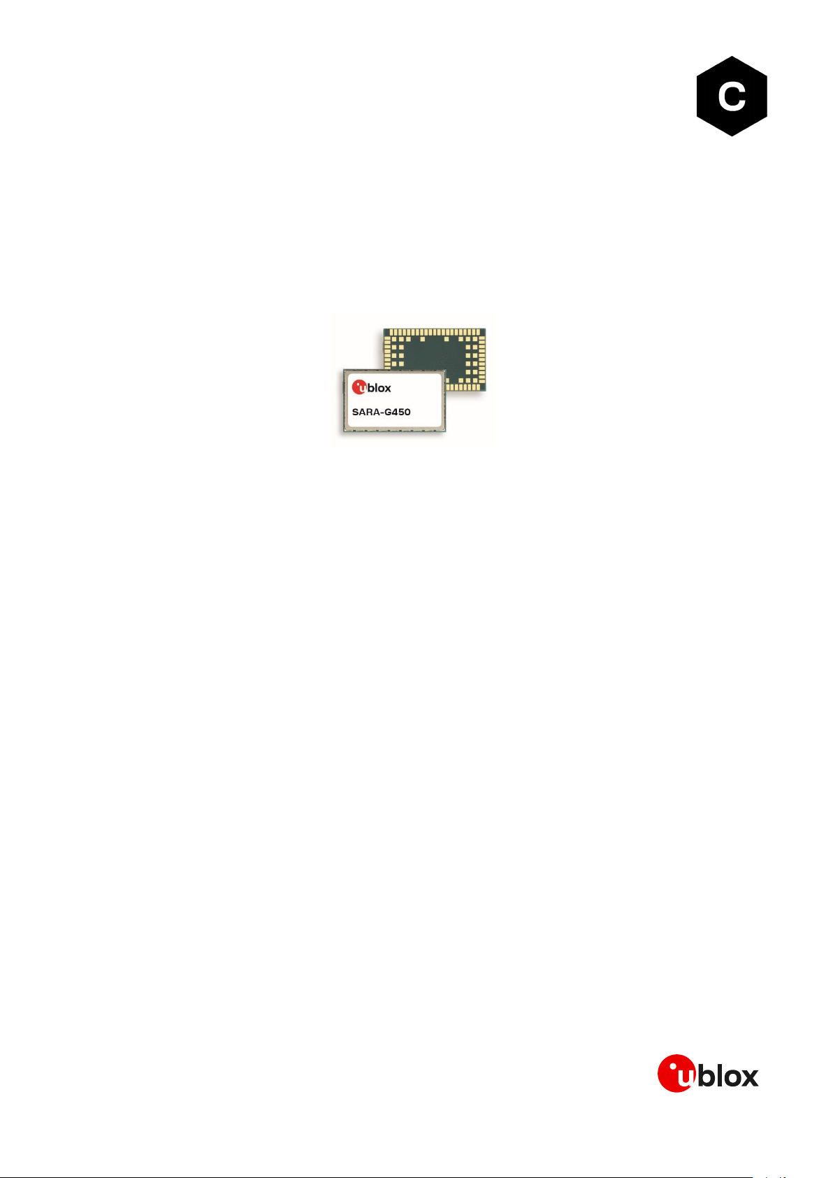
SARA-G450
Quad-band GSM/GPRS module
Data sheet
Abstract
Technical data sheet describing the SARA-G450 GSM/GPRS cellular modules. These modules are
complete and cost efficient solutions offering quad-band GSM/GPRS voice and/or data transmission
technology in a compact form factor.
SARA-G450 - Data sheet
UBX-18006165 - R11 Document information Page 2 of 39
C1-Public
Document information
Title
SARA-G450
Subtitle
Quad-band GSM/GPRS module
Document type
Data sheet
Document number
UBX-18006165
Revision and date
R11
08-Mar-2021
Disclosure restriction
C1-Public
Product status
Corresponding content status
Functional sample
Draft
For functional testing. Revised and supplementary data will be published later.
In development /
Prototype
Objective specification
Target values. Revised and supplementary data will be published later.
Engineering sample
Advance information
Data based on early testing. Revised and supplementary data will be published later.
Initial production
Early Production information
Data from product verification. Revised and supplementary data may be published later.
Mass production /
End of life
Production information
Document contains the final product specification.
This document applies to the following products:
Product name
Type number
Modem version
Application version
PCN reference
Product status
SARA-G450
SARA-G450-00C-00
09.02
A02.01
UBX-18067098
Obsolete
SARA-G450-00C-01
09.02
A03.17
UBX-20033037
Mass production
SARA-G450-01C-00
09.02
A04.23
UBX-20033037
End of life
SARA-G450-01C-01
09.02
A05.01
UBX-21006193
Mass production
u-blox or third parties may hold intellectual property rights in the products, names, logos and designs included in this document.
Copying, reproduction, modification or disclosure to third parties of this document or any part thereof is only permitted with the
express written permission of u-blox.
The information contained herein is provided “as is” and u-blox assumes no liability for its use. No warranty, either express or
implied, is given, including but not limited to, with respect to the accuracy, correctness, reliability and fitness for a particular
purpose of the information. This document may be revised by u-blox at any time without notice. For the most recent documents,
visit www.u-blox.com.
Copyright © u-blox AG.

SARA-G450 - Data sheet
UBX-18006165 - R11 Contents Page 3 of 39
C1-Public
Contents
Document information ................................................................................................................................ 2
Contents .......................................................................................................................................................... 3
1 Functional description ......................................................................................................................... 5
1.1 Overview ........................................................................................................................................................ 5
1.2 Product features ......................................................................................................................................... 5
1.3 Block diagram .............................................................................................................................................. 6
1.4 Product description .................................................................................................................................... 6
1.5 AT command support ................................................................................................................................ 7
1.6 Supported features .................................................................................................................................... 7
2 Interfaces .............................................................................................................................................. 10
2.1 Power management .................................................................................................................................10
2.1.1 Module supply input (VCC) .............................................................................................................10
2.1.2 RTC supply input/output (V_BCKP) ..............................................................................................10
2.1.3 Digital I/O interfaces supply output (V_INT) ...............................................................................10
2.2 Antenna .......................................................................................................................................................11
2.2.1 Antenna RF interface (ANT) ...........................................................................................................11
2.2.2 Antenna detection (ANT_DET) ......................................................................................................11
2.3 System functions ......................................................................................................................................11
2.3.1 Module power-on (PWR_ON) ..........................................................................................................11
2.3.2 Module power-off ..............................................................................................................................11
2.3.3 Module reset ......................................................................................................................................12
2.3.4 Digital I/O interfaces voltage selection (VSEL)...........................................................................12
2.4 SIM ...............................................................................................................................................................12
2.4.1 (U)SIM interface ................................................................................................................................12
2.4.2 SIM card detection (SIM_DET) .......................................................................................................12
2.5 Serial interfaces ........................................................................................................................................13
2.5.1 Asynchronous serial interface (UART) .........................................................................................13
2.5.2 Secondary auxiliary asynchronous serial interface (AUX UART) ............................................14
2.5.3 Additional asynchronous serial interface for FW upgrade and tracing (FT UART) ............15
2.5.4 DDC (I2C compatible) interface .....................................................................................................15
2.6 Audio interface ..........................................................................................................................................15
2.7 GPIO .............................................................................................................................................................16
3 Pin definition ........................................................................................................................................ 17
3.1 Pin assignment ..........................................................................................................................................17
4 Electrical specifications ................................................................................................................... 21
4.1 Absolute maximum rating.......................................................................................................................21
4.1.1 Maximum ESD ...................................................................................................................................22
4.2 Operating conditions ................................................................................................................................22
4.2.1 Operating temperature range ........................................................................................................22
4.2.2 Supply/Power pins ............................................................................................................................22

SARA-G450 - Data sheet
UBX-18006165 - R11 Contents Page 4 of 39
C1-Public
4.2.3 Current consumption .......................................................................................................................23
4.2.4 RF performance ................................................................................................................................24
4.2.5 ANT_DET pin ......................................................................................................................................24
4.2.6 PWR_ON pin .......................................................................................................................................24
4.2.7 PWR_OFF pin .....................................................................................................................................24
4.2.8 SIM pins ..............................................................................................................................................25
4.2.9 Generic Digital Interfaces pins .......................................................................................................25
4.2.10 DDC (I2C) pins ....................................................................................................................................26
4.2.11 Audio pins ...........................................................................................................................................26
5 Mechanical specifications ............................................................................................................... 28
6 Qualification and approvals............................................................................................................. 30
6.1 Reliability tests ..........................................................................................................................................30
6.2 Approvals ....................................................................................................................................................30
7 Product handling ................................................................................................................................. 31
7.1 Packaging ...................................................................................................................................................31
7.1.1 Reels ....................................................................................................................................................31
7.1.2 Tapes ...................................................................................................................................................32
7.2 Moisture sensitivity levels .......................................................................................................................33
7.3 Reflow soldering ........................................................................................................................................33
7.4 ESD precautions ........................................................................................................................................33
8 Default settings .................................................................................................................................. 34
9 Labeling and ordering information ............................................................................................... 35
9.1 Product labeling .........................................................................................................................................35
9.2 Explanation of codes ................................................................................................................................35
9.3 Ordering information ................................................................................................................................36
Appendix ....................................................................................................................................................... 37
A Glossary ................................................................................................................................................. 37
Related documentation ........................................................................................................................... 39
Revision history .......................................................................................................................................... 39
Contact .......................................................................................................................................................... 40

SARA-G450 - Data sheet
UBX-18006165 - R11 Functional description Page 5 of 39
C1-Public
1 Functional description
1.1 Overview
SARA-G450 modules are versatile 2.5G GSM/GPRS cellular modules in the miniature SARA 96-pin
LGA (Land Grid Array) form factor (26.0 x 16.0 mm).
Featuring low power consumption, the SARA-G450 modules combine baseband, RF transceiver,
power management unit, and power amplifier in a single solution allowing an easy integration into
compact designs and a seamless drop-in migration from other u-blox cellular module families
supporting 2G, 3G, LTE and LPWA (Cat M1 and Cat NB1) radio access technologies.
SARA-G450 modules provide a fully qualified and certified solution, reducing cost and enabling short
time to market. These modules are ideally suited for M2M applications such as: Automatic Meter
Reading (AMR), Remote Monitoring Automation and Control (RMAC), surveillance and security, road
pricing, asset tracking, fleet management, anti-theft systems and Point of Sales (PoS) terminals.
SARA-G450 modules are full-feature GSM/GPRS quad band cellular modules with a comprehensive
feature set including an extensive set of internet protocols. The modules are also designed to provide
fully integrated access to u-blox GNSS positioning chips and modules, with embedded A-GPS
(AssistNow Online and AssistNow Offline) functionality. Any host processor connected to the cellular
module through a single serial port can control both the cellular module and the positioning
chip / module.
The SARA-G450 modules’ compact form factor and LGA pads allow fully automated assembly with
standard pick & place and reflow soldering equipment for cost-efficient, high-volume production.
1.2 Product features
Model
Data
rate
Bands
Interfaces
Audio
Features
Grade
GPRS multi
-slot class
12
GSM/GPRS 4
-band
UART
SPI
USB 2.0 DDC (I
2C)
GPIO
Analog audio Digital audio Network indication Antenna supervisor Jamming detection Embedded TCP/UDP Embedded HTTP, FTP Embedded SSL / TLS GNSS via modem AssistNow
software
CellLocate® FW update via serial FOTA
Dual stack IPv4 / IPv6 Standard Professional Automotive
SARA-G450
● ● ●
□ ● □ ● ● □ ● ● ● □ □ □
● ●
●
● = supported by all FW versions
□ = supported by product version “01” onwards
Table 1: SARA-G450 modules’ main features summary
SARA-G450 - Data sheet
UBX-18006165 - R11 Functional description Page 6 of 39
C1-Public
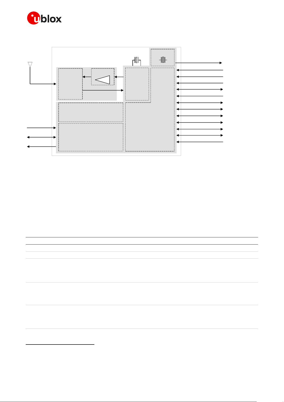
1.3 Block diagram
V_BCKP (RTC)
V_INT (I/O)
26 MHz
32.768 kHz
RF
transceiver
Power
management
Baseband
ANT
Switch
PA
VCC (supply)
Memory
Power-off
Power-on
SIM card
SIM card detection
UART (primary main)
UART (secondary auxiliary)
DDC (I2C)
Analog audio (MIC & SPK)
GPIOs
Antenna detection
VSEL (I/O voltage selection)
UART (flashing & tracing)
32.768 kHz over GPIO
Figure 1: SARA-G450 modules’ block diagram
☞ SARA-G450-00C modules, i.e. the “00” product version of the SARA-G450 modules, do not
support the following interfaces, which should be left unconnected and should not be driven by
external devices:
o Secondary auxiliary UART interface
o DDC (I2C) interface
o Analog audio interface
1.4 Product description
Item
SARA-G450
Mobile Station Class
B1
GSM/GPRS Protocol Stack
3GPP Release 99
GSM/GPRS bands
GSM 850 MHz
E-GSM 900 MHz
DCS 1800 MHz
PCS 1900 MHz
GSM/GPRS Power Class
Class 4 (33 dBm)
for 850/900 bands
Class 1 (30 dBm)
for 1800/1900 bands
Packet Switched Data Rate
GPRS multi-slot class 122
Coding scheme CS1-CS4
Up to 85.6 kb/s DL3
Up to 85.6 kb/s UL3
Table 2: SARA-G450 modules’ GSM/GPRS characteristics summary
1
Device can be attached to GPRS and GSM services (i.e. Packet Switch and Circuit Switch mode) using one service at a time.
2
GPRS multi-slot class 12 implies a maximum of 4 slots in Down-Link (reception) and 4 slots in Up-Link (transmission) with 5
slots in total. The SARA-G450 modules can be configured as GPRS multi-slot class 10 by means of AT command.
3
The maximum bit rate of the module depends on the current network settings.

SARA-G450 - Data sheet
UBX-18006165 - R11 Functional description Page 7 of 39
C1-Public
The network automatically configures the channel encoding used by the module, depending on
conditions and the quality of the radio link between cell phone and base station. If the channel is very
noisy, the network may use the most robust coding scheme (CS-1) to ensure higher reliability. If the
channel provides good conditions, the network can use the least robust but fastest coding scheme
(CS-4) to obtain optimum speed.
1.5 AT command support
The module supports AT commands according to 3GPP standards TS 27.007 [6], 27.005 [7] and
27.010 [8], plus u-blox proprietary AT commands.
☞ For the complete list of the supported AT commands and their syntax, see the u-blox AT
commands manual [2].
1.6 Supported features
Table 3 lists some of the main features supported by SARA-G450 modules.
Feature
Description
Network indication
GPIO configured to indicate the network status: registered home network, registered
roaming, voice or data call enabled, no service.
The network indication feature can be enabled through a custom AT command (see the
u-blox AT commands manual [2], +UGPIOC AT command).
Antenna detection
The ANT_DET pin provides antenna presence detection capability, evaluating the
resistance from the ANT pin to GND by means of an external antenna detection circuit
implemented on the application board.
The antenna detection feature can be enabled through a custom AT command (see the
u-blox AT commands manual [2], +UANTR AT command).
Jamming detection4
Detects “artificial” interference that obscures the operator’s carriers providing access to
the GSM service and reports the start and stop of such conditions to the application
processor (AP). The AP can react appropriately, e.g. by switching off the radio
transceiver to reduce power consumption and monitoring the environment at constant
periods.
The jamming detection feature can be enabled and configured through a custom AT
command (see the u-blox AT commands manual [2], +UCD AT command).
Second AT interface4
AT command and data mode available on both the primary main UART interface and the
secondary auxiliary UART interface.
See the u-blox AT commands manual [2], +USIO AT command, for further details
regarding serial interfaces configuration selection.
Embedded TCP/IP and UDP/IP
Embedded TCP/IP and UDP/IP stack including direct link mode for TCP and UDP sockets.
The sockets can be configured in direct link mode to establish a transparent end-to-end
communication with an already connected TCP or UDP socket via serial interface.
FTP, FTPS
File Transfer Protocol as well as Secure File Transfer Protocol (SSL encryption of FTP
control channel) functionalities are supported via AT commands.
HTTP, HTTPS
Hyper-Text Transfer Protocol as well as Secure Hyper-Text Transfer Protocol (SSL
encryption) functionalities are supported via AT commands. HEAD, GET, POST, DELETE
and PUT operations are available. Up to 4 client contexts can be simultaneously used.
Embedded TLS 1.2
With the support of X.509 certificates, Embedded TLS 1.2 provides server and client
authentication, data encryption, data signature and enables TCP/IP applications like
HTTPS and FTPS to communicate over a secured and trusted connection.
The feature can be configured and enabled by +USECMNG and +USECPRF AT
commands.
4
Not supported by “00” product version

SARA-G450 - Data sheet
UBX-18006165 - R11 Functional description Page 8 of 39
C1-Public
Feature
Description
IPv4/IPv6 dual-stack
Capability to move between IPv4 and dual stack network infrastructures. IPv4 and IPv6
addresses can be used.
GPS/GNSS via modem4
Full access to u-blox positioning chips and modules is available through a dedicated DDC
(I2C) interface. A single serial port from any host processor can control both the u-blox
SARA-G450 cellular module and the u-blox positioning chip / module.
AssistNow software4
Embedded AssistNow Online and AssistNow Offline clients to provide full developed to
provide better GNSS performance and faster Time-to-First-Fix.
The clients can be enabled / disabled with an AT command.
CellLocate®4
Enables the estimation of device position based on the parameters of the mobile
network cells visible to the specific device based on the CellLocate® database:
• Normal scan: parameters of the visible home network cells are only sent
• Deep scan: parameters of all surrounding cells of all mobile operators are sent
CellLocate® is implemented using a set of AT commands for CellLocate® service
configuration and position request.
Hybrid positioning5
Provides the module’s current position using a u-blox positioning chip or module or the
estimated position from CellLocate®, depending on which positioning method provides
the best and fastest solution according to the user configuration.
Hybrid positioning is implemented through a set of AT commands that allow the
configuration and the position request.
Firmware update Over AT
commands (FOAT)
Firmware module upgrade over the UART interface, using AT command.
DTMF decoder5
During a voice call, the Dual-Tone Multi-Frequency detector analyses the Rx speech
(coming from remote party). The detected DTMF symbols can be output via related
URC.
See the u-blox AT commands manual [2], +UDTMFD AT command, for further details.
Smart temperature supervisor5
Constant monitoring of the module board temperature:
• Warning notification when the temperature approaches an upper or lower predefined
threshold
• Shutdown notified and forced when the temperature value is outside the specified
range (shutdown suspended in case of an emergency call in progress)
The smart temperature supervisor feature can be enabled or disabled through an AT
command (see the u-blox AT commands manual [2], +USTS AT command).
☞ The sensor measures board temperature inside the shield, which can differ from
ambient temperature.
Power saving
The power saving configuration is by default disabled, but it can be configured using an
AT command.
When power saving is enabled, the module automatically enters the low power idle-mode
whenever possible, reducing current consumption.
During the idle-mode, the module processor core runs with the RTC 32 kHz reference
clock, which is generated by the internal 32 kHz oscillator.
For more details, see the SARA-G450 system integration manual [1] and the u-blox AT
commands manual [2], +UPSV AT command.
Last gasp5
In case of power supply outage (i.e. main supply interruption, battery removal, battery
voltage below a certain threshold) the cellular module can be configured to send an
alarm notification to a remote entity.
The feature can be enabled and configured through the +ULGASP AT command.
Table 3: SARA-G450 modules main supported features
☞ u-blox is extremely mindful of user privacy. When a position is sent to the CellLocate
®
server, u-blox
is unable to track the SIM used or the specific device.
5
Not supported by “00” product version

SARA-G450 - Data sheet
UBX-18006165 - R11 Interfaces Page 9 of 39
C1-Public
2 Interfaces
2.1 Power management
2.1.1 Module supply input (VCC)
SARA-G450 modules must be supplied through the three VCC pins by a DC power supply. Voltages
must be stable: during operation, the current drawn from VCC can vary by some order of magnitude,
especially due to the surging consumption profile of the GSM system (described in the SARA-G450
system integration manual [1]).
SARA-G450 modules provide separate supply inputs over the three VCC pins:
• VCC pins #52 and #53 represent the supply input for the internal RF power amplifier, demanding
most of the total current drawn of the module when RF transmission is enabled during a call
• VCC pin #51 represents the supply input for the internal baseband Power Management Unit,
demanding minor part of the total current drawn of the module when RF transmission is enabled
during a call
It is important that the system power supply circuit is able to withstand the maximum pulse current
during a transmit burst at maximum power level (see Table 11).
2.1.2 RTC supply input/output (V_BCKP)
V_BCKP is the Real Time Clock (RTC) supply of SARA-G450 modules. When VCC voltage is within the
valid operating range, the internal Power Management Unit (PMU) supplies the RTC and the same
supply voltage is available on V_BCKP pin. If the VCC voltage is under the minimum operating limit
(e.g. during not powered mode), V_BCKP pin can externally supply the RTC.
2.1.3 Digital I/O interfaces supply output (V_INT)
SARA-G450 modules provide supply rail output on the V_INT pin, which is internally generated when
the module is switched on. The same voltage domain is used internally to supply the generic digital
I/O interfaces of the modules (UART interfaces, I2C interface and GPIO pins).
The voltage value of the V_INT supply output can be set to 1.8 V or 3 V according to the configuration
of the VSEL input pin (see section 2.3.4). The V_INT supply output can be used in place of an external
regulator.
☞ It is recommended to provide a Test-Point connected to the V_INT pin for diagnostic purpose.

SARA-G450 - Data sheet
UBX-18006165 - R11 Interfaces Page 10 of 39
C1-Public
2.2 Antenna
2.2.1 Antenna RF interface (ANT)
The ANT pin has an impedance of 50 and provides the RF antenna interface of SARA-G450 modules.
2.2.2 Antenna detection (ANT_DET)
The ANT_DET pin is an Analog to Digital Converter (ADC) input to sense the antenna presence (as
optional feature), evaluating the resistance from the ANT pin to GND by means of an external antenna
detection circuit implemented on the application board. For more details, see the SARA-G450 system
integration manual [1] and the u-blox AT commands manual [2], +UANTR AT command.
2.3 System functions
2.3.1 Module power-on (PWR_ON)
SARA-G450 modules can be switched on in one of the following ways:
• Low level on the PWR_ON input pin, i.e. forcing the pin (normally high due to internal pull-up) to a
low level for a valid time period (see section 4.2.6). The PWR_ON line is intended to be driven by
open drain, open collector or contact switch.
• RTC alarm, i.e. pre-programmed scheduled time (see the u-blox AT commands manual [2], +CALA
AT command)
☞ It is recommended to provide a Test-Point connected to the PWR_ON pin for diagnostic purpose.
2.3.2 Module power-off
SARA-G450 modules can be properly switched off, with storage of current settings and network
detach, by:
• AT+CPWROFF command (see the u-blox AT commands manual [2]).
An abrupt hardware shutdown occurs when a low level is applied to the PWR_OFF pin, which is
normally set high, for a valid time period (see section 4.2.7), but in this case the module does not
perform the storing of the current parameter settings as well as the proper network detach. The
PWR_OFF line is intended to be driven by open drain, open collector or contact switch.
An abrupt under-voltage shutdown occurs on SARA-G450 modules when the VCC supply drops below
the extended operating range minimum limit, but in this case it is not possible to perform the storing
of the current parameter settings in the module’s non-volatile memory as well as the proper network
detach.
An over-temperature or an under-temperature shutdown occurs on SARA-G450 modules when the
temperature measured within the cellular module reaches the dangerous area, if the optional smart
temperature supervisor feature is enabled and configured by the dedicated AT command. For more
details, see the SARA-G450 system integration manual [1] and the u-blox AT commands manual [2],
+USTS AT command.
☞ The smart temperature supervisor feature is not supported by “00” product version.
☞ It is recommended to provide a test-point connected to the PWR_OFF pin for diagnostic purpose.

SARA-G450 - Data sheet
UBX-18006165 - R11 Interfaces Page 11 of 39
C1-Public
2.3.3 Module reset
SARA-G450 modules can be properly reset (rebooted), with storage of current parameter settings in
the module’s non-volatile memory and proper network detach, by:
• AT+CFUN command (see the u-blox AT commands manual [2]). This causes an “internal” or
“software” reset of the module.
An abrupt hardware shutdown occurs when a low level is applied to the PWR_OFF pin, which is
normally set high, for a valid time period (see section 4.2.7), but in this case the module does not
perform the storing of the current parameter settings in the module’s non-volatile memory as well as
the proper network detach. The module can be subsequently rebooted forcing a low level at the
PWR_ON input pin for a valid time period (see section 4.2.6).
2.3.4 Digital I/O interfaces voltage selection (VSEL)
The digital I/O interfaces of SARA-G450 modules (the UART interfaces, I2C interface and GPIO pins)
can operate at 1.8 V or 3 V voltage rail. The operating voltage can be selected using the VSEL input
pin:
• If VSEL input pin is connected to GND, the digital I/O interfaces operate at 1.8 V
• If VSEL input pin is left unconnected, the digital I/O interfaces operate at 3 V
The operating voltage cannot be changed dynamically: the VSEL input pin configuration has to be set
before the boot of SARA-G450 modules and then it cannot be changed after switched on.
2.4 SIM
2.4.1 (U)SIM interface
A (U)SIM card interface is available via the VSIM, SIM_IO, SIM_CLK, SIM_RST pins of SARA-G450
modules for the direct connection of an external SIM card/chip: the high-speed SIM/ME interface is
implemented as well as the automatic detection of the required SIM supporting voltage.
Both 1.8 V and 3 V SIM types are supported: activation and deactivation with automatic voltage
switch from 1.8 V to 3 V are implemented, according to ISO-IEC 7816-3 specifications.
2.4.2 SIM card detection (SIM_DET)
The SIM_DET pin of SARA-G450 modules is a digital input provided to sense the SIM card presence
(as an optional feature), when it is properly connected to the mechanical switch of the SIM card holder
(for more details see the SARA-G450 system integration manual [1]).

SARA-G450 - Data sheet
UBX-18006165 - R11 Interfaces Page 12 of 39
C1-Public
2.5 Serial interfaces
SARA-G450 modules provide the following serial communication interfaces:
• UART interface: 9-wire unbalanced 1.8 V / 3 V asynchronous serial interface supporting:
o AT command mode
6
o Data mode and online command mode
6
o MUX functionality, including dedicated GNSS tunneling virtual channel
7
o FW upgrades by means of the FOAT feature
• Secondary auxiliary UART interface
8
: 3-wire unbalanced 1.8 V / 3 V asynchronous serial interface
supporting:
o AT command mode
6
o Data mode and online command mode
6
o GNSS tunneling
• Additional UART interface for FW upgrade and tracing: 3-wire unbalanced 1.8 V / 3 V
asynchronous serial interfaces supporting:
o FW upgrades by means of the dedicated tool
o Trace log capture (diagnostic purpose)
• DDC interface
9
: I2C-bus compatible 1.8 V / 3 V interface supporting:
o Communication with u-blox GNSS positioning chips / modules
2.5.1 Asynchronous serial interface (UART)
The UART interface is a 9-wire unbalanced asynchronous serial interface, supporting:
• AT command mode
6
• Data mode and online command mode
6
• MUX functionality (see 2.5.1.1)
• FW upgrades by means of the FOAT feature
UART characteristics are:
• Complete serial port with RS-232 functionality conforming to ITU-T V.24 recommendation [5],
with CMOS compatible signal levels (0 V for low data bit or ON state and 1.8 V / 3 V for high data
bit or OFF state)
• Data lines (RXD as output, TXD as input), hardware flow control lines (CTS as output, RTS as
input), modem status and control lines (DTR as input, DSR as output, DCD as output, RI as output)
are provided
• Hardware flow control (default value) or none flow control are supported
• Power saving indication available on the hardware flow control output (CTS line): the line is driven
to the OFF state when the module is not ready to accept data signals
• 2400, 4800, 9600, 19200, 38400, 57600, 115200 bit/s baud rates are supported
• One-shot auto baud rate detection (autobauding) is the default configuration
• Frame format can be: 8N1 (8 data bits, no parity, 1 stop bit), or 8N2 (8 data bits, no parity, 2 stop
bits), or 8E1 (8 data bits, even parity, 1 stop bit), or 8O1 (8 data bits, odd parity, 1 stop bit)
• Default frame configuration is 8N1 (8 data bits, no parity, 1 stop bit)
6
See the u-blox AT commands manual [2] for the definition of the command mode, data mode, and online command mode.
7
GNSS tunneling is not supported by “00” product version
8
Secondary auxiliary UART interface is not supported by “00” product version.
9
DDC I2C-bus compatible interface is not supported by “00” product version.
 Loading...