

Ublox SARA-U201 ATEX, SARA-G350, SARA-U260, SARA-G310, SARA-U270 System Integration Manual
...Page 1

Abstract
This document describes the features and the system integration of
the SARA-G3 series GSM/GPRS cellular modules and the SARA-U2
GSM/EGPRS/HSPA cellular modules.
These modules are complete and cost efficient solutions offering
voice and/or data communication over diverse cellular radio access
technologies in the same compact SARA form factor: the SARA-G3
series support up to four GSM/GPRS bands, while the SARA-U2
series support up to five high-speed HSPA bands and up to four
GSM/EGPRS bands.
www.u-blox.com
UBX-13000995 - R26
SARA-G3 and SARA-U2 series
GSM/GPRS and GSM/EGPRS/HSPA
Cellular Modules
System Integration Manual
Page 2

SARA-G3 and SARA-U2 series - System Integration Manual
Document Information
Title
SARA-G3 and SARA-U2 series
Subtitle
GSM/GPRS and GSM/EGPRS/HSPA Cellular Modules
Document type
System Integration Manual
Document number
UBX-13000995
Revision and date
R26
02-Jan-2018
Disclosure restriction
u-blox reserves all rights to this document and the information contained herein. Products, names, logos and designs described herein may in
whole or in part be subject to intellectual property rights. Reproduction, use, modification or disclosure to third parties of this document or
any part thereof without the express permission of u-blox is strictly prohibited.
The information contained herein is provided “as is” and u-blox assumes no liability for the use of the information. No warranty, either
express or implied, is given, including but not limited, with respect to the accuracy, correctness, reliability and fitness for a particular purpose
of the information. This document may be revised by u-blox at any time. For most recent documents, visit www.u-blox.com.
Copyright © 2018, u-blox AG
u-blox is a registered trademark of u-blox Holding AG in the EU and other countries.
Microsoft and Windows are either registered trademarks or trademarks of Microsoft Corporation in the United States and/or other countries.
All other registered trademarks or trademarks mentioned in this document are property of their respective owners.
UBX-13000995 - R26
Page 2 of 217
Page 3

This document applies to the following products:
Name
Type number
Modem version
Application version
PCN reference
SARA-G300
SARA-G300-00S-00
08.58
N.A.
GSM.G2-TN-13007
SARA-G300-00S-01
08.58
A01.01
UBX-16010060
SARA-G310
SARA-G310-00S-00
08.58
N.A.
GSM.G2-TN-13007
SARA-G310-00S-01
08.58
A01.01
UBX-16010060
SARA-G340
SARA-G340-00S-00
08.49
N.A.
UBX-14000382
SARA-G340-01S-00
08.70
A00.02
UBX-14039634
SARA-G340-02S-00
08.90
A00.02
UBX-16001074
SARA-G340 ATEX
SARA-G340-02X-00
08.90
A00.02
TBD
SARA-G350
SARA-G350-00S-00
08.49
N.A.
GSM.G2-TN-13002
SARA-G350-01S-00
08.70
A00.02
UBX-14039634
SARA-G350-01B-00
08.70
A00.02
TBD SARA-G350-02A-01
08.90
A00.06
UBX-17003537
SARA-G350-02S-00
08.90
A00.02
UBX-16001074
SARA-G350 ATEX
SARA-G350-00X-00
08.49
N.A.
GSM.G2-TN-13002
SARA-G350-02X-00
08.90
A00.02
UBX-17048555
SARA-U201
SARA-U201-03A-00
23.60
A01.02
UBX-17012748
SARA-U201-03B-00
23.60
A01.01
UBX-16018086
SARA-U201-63B-00
23.62
A01.01
UBX-17053345
SARA-U201-04A-00
23.60
A01.06
UBX-17058162
SARA-U201-04B-00
23.60
A01.06
UBX-17058162
SARA-U201 ATEX
SARA-U201-03X-00
23.60
A01.01
UBX-16030157
SARA-U201-04X-00
23.60
A01.06
UBX-17058162
SARA-U260
SARA-U260-00S-01
23.20
A01.01
UBX-15013844
SARA-U260-00S-02
23.20
A01.02
UBX-17061316
SARA-U260-03S-00
23.41
A01.01
UBX-15020745
SARA-U260-03S-01
23.41
A01.02
UBX-17061316
SARA-U270
SARA-U270-00S-01
23.20
A01.01
UBX-16006754
SARA-U270-00S-02
23.20
A01.02
UBX-17061316
SARA-U270-03A-00
23.41
A01.01
UBX-17004455
SARA-U270-03A-01
23.41
A01.02
UBX-17064001
SARA-U270-03S-00
23.41
A01.01
UBX-15020745
SARA-U270-03S-01
23.41
A01.02
UBX-17061316
SARA-U270-73S-00
23.41
A01.02
UBX-16028821
SARA-U270-73S-01
23.41
A01.03
UBX-17061316
SARA-U270-53S-00
23.41
A01.03
UBX-16008757
SARA-U270-53S-01
23.41
A01.04
UBX-17011151
SARA-U270-53S-02
23.41
A01.05
UBX-17061316
SARA-U270 ATEX
SARA-U270-00X-00
23.20
A01.00
UBX-14015739
SARA-U270-00X-01
23.20
A01.02
UBX-17061316
SARA-U280
SARA-U280-00S-00
23.28
A01.00
UBX-15013708
SARA-U280-00S-01
23.28
A01.01
UBX-17061316
SARA-U280-03S-00
23.41
A01.01
UBX-15020745
SARA-U280-03S-01
23.41
A01.02
UBX-17061316
SARA-G3 and SARA-U2 series - System Integration Manual
UBX-13000995 - R26 Preface
Page 3 of 217
Page 4

SARA-G3 and SARA-U2 series - System Integration Manual
Preface
u-blox Technical Documentation
As part of our commitment to customer support, u-blox maintains an extensive volume of technical
documentation for our products. In addition to our product-specific technical data sheets, the following manuals
are available to assist u-blox customers in product design and development.
AT Commands Manual: This document provides the description of the AT commands supported by the
u-blox cellular modules.
System Integration Manual: This document provides the description of u-blox cellular modules’ system
from the hardware and the software points of view, it provides hardware design guidelines for the optimal
integration of the cellular modules in the application device, and it provides information on how to set up
production and final product tests on application devices which integrate the cellular modules.
Application Notes: These documents provide guidelines and information on specific hardware and/or
software topics on u-blox cellular modules. See the Related documents section for a list of application notes
related to your cellular module.
How to use this Manual
The SARA-G3 and SARA-U2 series System Integration Manual provides the necessary information to successfully
design in and configure these u-blox cellular modules.
This manual has a modular structure. It is not necessary to read it from the beginning to the end.
The following symbols are used to highlight important information within the manual:
An index finger points out key information pertaining to module integration and performance.
A warning symbol indicates actions that could negatively impact or damage the module.
Questions
If you have any questions about u-blox cellular Integration:
Read this manual carefully.
Contact our information service on the homepage http://www.u-blox.com
Technical Support
Worldwide Web
Our website (http://www.u-blox.com) is a rich pool of information. Product information and technical documents
can be accessed 24 hours a day.
By E-mail
If you have technical problems or cannot find the required information in the provided documents, contact the
closest Technical Support office. To ensure that we process your request as soon as possible, use our service pool
email addresses rather than personal staff email addresses. Contact details are at the end of the document.
Helpful Information when Contacting Technical Support
When contacting Technical Support, have the following information ready:
Module type (e.g. SARA-G350) and firmware version
Module configuration
A clear description of your question or the problem
A short description of the application
Your complete contact details
UBX-13000995 - R26 Preface
Page 4 of 217
Page 5

SARA-G3 and SARA-U2 series - System Integration Manual
Contents
Preface ................................................................................................................................ 4
Contents .............................................................................................................................. 5
1 System description ..................................................................................................... 10
1.1 Overview ............................................................................................................................................ 10
1.2 Architecture ........................................................................................................................................ 13
1.2.1 Internal blocks ............................................................................................................................. 15
1.3 Pin-out ............................................................................................................................................... 17
1.4 Operating modes ................................................................................................................................ 22
1.5 Supply interfaces ................................................................................................................................ 24
1.5.1 Module supply input (VCC) ......................................................................................................... 24
1.5.2 RTC supply input/output (V_BCKP) .............................................................................................. 33
1.5.3 Generic digital interfaces supply output (V_INT) ........................................................................... 34
1.6 System function interfaces .................................................................................................................. 35
1.6.1 Module power-on ....................................................................................................................... 35
1.6.2 Module power-off ....................................................................................................................... 39
1.6.3 Module reset ............................................................................................................................... 41
1.6.4 External 32 kHz signal input (EXT32K) ......................................................................................... 42
1.6.5 Internal 32 kHz signal output (32K_OUT) .................................................................................... 42
1.7 Antenna interface ............................................................................................................................... 43
1.7.1 Antenna RF interface (ANT) ......................................................................................................... 43
1.7.2 Antenna detection interface (ANT_DET) ...................................................................................... 44
1.8 SIM interface ...................................................................................................................................... 44
1.8.1 (U)SIM card interface ................................................................................................................... 44
1.8.2 SIM card detection interface (SIM_DET) ....................................................................................... 44
1.9 Serial interfaces .................................................................................................................................. 45
1.9.1 Asynchronous serial interface (UART) .......................................................................................... 46
1.9.2 Auxiliary asynchronous serial interface (AUX UART) ..................................................................... 59
1.9.3 USB interface .............................................................................................................................. 63
1.9.4 DDC (I2C) interface ...................................................................................................................... 66
1.10 Audio interface ............................................................................................................................... 68
1.10.1 Analog audio interface ................................................................................................................ 68
1.10.2 Digital audio interface ................................................................................................................. 70
1.10.3 Voice-band processing system ..................................................................................................... 72
1.11 General Purpose Input/Output (GPIO) ............................................................................................. 76
1.12 Reserved pins (RSVD) ...................................................................................................................... 80
1.13 System features............................................................................................................................... 81
1.13.1 Network indication ...................................................................................................................... 81
1.13.2 Antenna detection ...................................................................................................................... 81
1.13.3 Jamming detection ...................................................................................................................... 81
UBX-13000995 - R26 Contents
Page 5 of 217
Page 6

SARA-G3 and SARA-U2 series - System Integration Manual
1.13.4 TCP/IP and UDP/IP ....................................................................................................................... 82
1.13.5 FTP .............................................................................................................................................. 82
1.13.6 HTTP ........................................................................................................................................... 82
1.13.7 SMTP ........................................................................................................................................... 82
1.13.8 SSL/TLS ........................................................................................................................................ 83
1.13.9 Dual stack IPv4/IPv6 ..................................................................................................................... 85
1.13.10 Smart temperature management ............................................................................................. 86
1.13.11 AssistNow clients and GNSS integration ................................................................................... 89
1.13.12 Hybrid positioning and CellLocate® .......................................................................................... 89
1.13.13 Control Plane Aiding / Location Services (LCS) .......................................................................... 92
1.13.14 Bearer Independent Protocol.................................................................................................... 92
1.13.15 Multi-Level Precedence and Pre-emption Service ...................................................................... 92
1.13.16 Network Friendly Mode ........................................................................................................... 92
1.13.17 Firmware upgrade Over AT (FOAT) .......................................................................................... 93
1.13.18 Firmware update Over The Air (FOTA) ...................................................................................... 93
1.13.19 Last gasp ................................................................................................................................. 93
1.13.20 Smart radio Coverage Manager ............................................................................................... 94
1.13.21 In-Band modem (eCall / ERA-GLONASS) .................................................................................. 94
1.13.22 SIM Access Profile (SAP) ........................................................................................................... 95
1.13.23 Power Saving ........................................................................................................................... 96
2 Design-in ..................................................................................................................... 97
2.1 Overview ............................................................................................................................................ 97
2.2 Supply interfaces ................................................................................................................................ 98
2.2.1 Module supply (VCC) .................................................................................................................. 98
2.2.2 RTC supply (V_BCKP) ................................................................................................................. 112
2.2.3 Interface supply (V_INT) ............................................................................................................. 114
2.3 System functions interfaces .............................................................................................................. 115
2.3.1 Module power-on (PWR_ON) .................................................................................................... 115
2.3.2 Module reset (RESET_N) ............................................................................................................ 116
2.3.3 32 kHz signal (EXT32K and 32K_OUT) ....................................................................................... 117
2.4 Antenna interface ............................................................................................................................. 118
2.4.1 Antenna RF interface (ANT) ....................................................................................................... 118
2.4.2 Antenna detection interface (ANT_DET) .................................................................................... 125
2.5 SIM interface .................................................................................................................................... 128
2.6 Serial interfaces ................................................................................................................................ 134
2.6.1 Asynchronous serial interface (UART) ........................................................................................ 134
2.6.2 Auxiliary asynchronous serial interface (UART AUX) ................................................................... 140
2.6.3 Universal Serial Bus (USB) .......................................................................................................... 142
2.6.4 DDC (I2C) interface .................................................................................................................... 144
2.7 Audio interface ................................................................................................................................. 149
2.7.1 Analog audio interface .............................................................................................................. 149
2.7.2 Digital audio interface ............................................................................................................... 156
2.8 General Purpose Input/Output (GPIO) ............................................................................................... 159
UBX-13000995 - R26 Contents
Page 6 of 217
Page 7

SARA-G3 and SARA-U2 series - System Integration Manual
2.9 Reserved pins (RSVD) ........................................................................................................................ 160
2.10 Module placement ........................................................................................................................ 160
2.11 Module footprint and paste mask ................................................................................................. 161
2.12 Thermal guidelines ........................................................................................................................ 162
2.13 ESD guidelines .............................................................................................................................. 164
2.13.1 ESD immunity test overview ...................................................................................................... 164
2.13.2 ESD immunity test of u-blox SARA-G3 and SARA-U2 reference designs ..................................... 164
2.13.3 ESD application circuits .............................................................................................................. 165
2.14 SARA-G3 / SARA-U2 ATEX modules integration in devices intended for use in potentially explosive
atmospheres ................................................................................................................................................ 167
2.14.1 General guidelines ..................................................................................................................... 167
2.14.2 Guidelines for VCC supply circuit design ................................................................................... 168
2.14.3 Guidelines for antenna RF interface design ................................................................................ 170
2.15 Schematic for SARA-G3 and SARA-U2 series module integration .................................................. 171
2.15.1 Schematic for SARA-G300 / SARA-G310 modules integration ................................................... 171
2.15.2 Schematic for SARA-G340 / SARA-G350 modules integration ................................................... 172
2.15.3 Schematic for SARA-U2 series modules integration ................................................................... 173
2.16 Design-in checklist ........................................................................................................................ 174
2.16.1 Schematic checklist ................................................................................................................... 174
2.16.2 Layout checklist ......................................................................................................................... 175
2.16.3 Antenna checklist ...................................................................................................................... 175
3 Handling and soldering ........................................................................................... 176
3.1 Packaging, shipping, storage and moisture preconditioning ............................................................. 176
3.2 Handling ........................................................................................................................................... 176
3.3 Soldering .......................................................................................................................................... 177
3.3.1 Soldering paste ......................................................................................................................... 177
3.3.2 Reflow soldering ....................................................................................................................... 177
3.3.3 Optical inspection ...................................................................................................................... 178
3.3.4 Cleaning .................................................................................................................................... 178
3.3.5 Repeated reflow soldering ......................................................................................................... 179
3.3.6 Wave soldering ......................................................................................................................... 179
3.3.7 Hand soldering .......................................................................................................................... 179
3.3.8 Rework ...................................................................................................................................... 179
3.3.9 Conformal coating .................................................................................................................... 179
3.3.10 Casting ...................................................................................................................................... 179
3.3.11 Grounding metal covers ............................................................................................................ 179
3.3.12 Use of ultrasonic processes ........................................................................................................ 179
4 Approvals .................................................................................................................. 180
4.1 Product certification approval overview............................................................................................. 180
4.2 US Federal Communications Commission notice ............................................................................... 181
4.2.1 Safety warnings review the structure ......................................................................................... 181
4.2.2 Declaration of conformity .......................................................................................................... 181
4.2.3 Modifications ............................................................................................................................ 182
UBX-13000995 - R26 Contents
Page 7 of 217
Page 8

SARA-G3 and SARA-U2 series - System Integration Manual
4.3 Innovation, Science and Economic Development Canada notice ....................................................... 182
4.3.1 Declaration of conformity .......................................................................................................... 182
4.3.2 Modifications ............................................................................................................................ 183
4.4 European conformance CE mark ...................................................................................................... 184
4.5 Brazilian Anatel certification ............................................................................................................. 186
4.6 Australian Regulatory Compliance Mark ........................................................................................... 186
4.7 Mexican IFT certification ................................................................................................................... 187
4.8 Chinese CCC mark ........................................................................................................................... 187
4.9 Korean KCC certification .................................................................................................................. 188
4.10 Taiwanese NCC certification ......................................................................................................... 188
4.11 Japanese Giteki certification .......................................................................................................... 188
4.12 SARA-G3 / SARA-U2 ATEX modules conformance for use in explosive atmospheres ..................... 189
5 Product testing ......................................................................................................... 191
5.1 u-blox in-series production test ......................................................................................................... 191
5.2 Test parameters for OEM manufacturers .......................................................................................... 191
5.2.1 “Go/No go” tests for integrated devices .................................................................................... 192
5.2.2 Functional tests providing RF operation ..................................................................................... 192
Appendix ........................................................................................................................ 195
A Migration between LISA and SARA-G3 modules ................................................... 195
A.1 Overview .......................................................................................................................................... 195
A.2 Checklist for migration ..................................................................................................................... 196
A.3 Software migration ........................................................................................................................... 198
A.4 Hardware migration ......................................................................................................................... 198
A.4.1 Supply interfaces ....................................................................................................................... 198
A.4.2 System functions interfaces ....................................................................................................... 199
A.4.3 Antenna interface ..................................................................................................................... 200
A.4.4 SIM interface ............................................................................................................................. 201
A.4.5 Serial interfaces ......................................................................................................................... 201
A.4.6 Audio interfaces ........................................................................................................................ 202
A.4.7 GPIO pins .................................................................................................................................. 203
A.4.8 Reserved pins ............................................................................................................................ 203
A.4.9 Pin-out comparison between LISA and SARA-G3 ....................................................................... 203
B Migration between SARA-G3 and SARA-U2 ........................................................... 208
B.1 Overview .......................................................................................................................................... 208
B.2 Pin-out comparison between SARA-G3 and SARA-U2 ...................................................................... 209
B.3 Schematic for SARA-G3 and SARA-U2 integration ............................................................................ 211
C Glossary .................................................................................................................... 212
Related documents ........................................................................................................ 214
Revision history .............................................................................................................. 216
UBX-13000995 - R26 Contents
Page 8 of 217
Page 9

SARA-G3 and SARA-U2 series - System Integration Manual
Contact ............................................................................................................................ 217
UBX-13000995 - R26 Contents
Page 9 of 217
Page 10

SARA-G3 and SARA-U2 series - System Integration Manual
1 System description
1.1 Overview
SARA-G3 series GSM/GPRS cellular modules and SARA-U2 series GSM/EGPRS/HSPA cellular modules are versatile
solutions offering voice and/or data communication over diverse radio access technologies in the same miniature
SARA LGA form factor (26 x 16 mm), which allows for seamless drop-in migration between the two SARA-G3
and SARA-U2 series and to and from the other u-blox cellular modules families.
SARA-G350 and SARA-G340 are respectively quad-band and dual-band full feature GSM/GPRS cellular modules
with a comprehensive feature set, including an extensive set of internet protocols and access to u-blox GNSS
positioning chips and modules with embedded A-GPS (AssistNow Online and AssistNow Offline) functionality.
SARA-G310 and SARA-G300 are respectively quad-band and dual-band GSM/GPRS cellular modules targeted for
high volume cost sensitive applications, providing GSM/GPRS functionalities with a reduced set of additional
features to minimize the customer’s total cost of ownership.
SARA-U2 series includes variants supporting various band combinations for worldwide operation, for North
America operation and for operation in Europe, Asia and other countries. A cost-saving UMTS-only variant is also
available.
All SARA-U2 series modules provide a rich feature set including an extensive set of internet protocols, dual-stack
IPv4 / IPv6 and access to u-blox GNSS positioning chips and modules, with embedded A-GPS (AssistNow Online
and AssistNow Offline) functionality.
UBX-13000995 - R26 System description
Page 10 of 217
Page 11

SARA-G3 and SARA-U2 series - System Integration Manual
Module
Data rate
Bands
Interfaces
Audio
Features
Grade
3G Up-Link [Mbit/s]
3G Down-Link [Mbit/s]
2G Up-Link [kbit/s]
2G Down-Link [kbit/s]
3G bands [MHz]
2G bands [MHz]
UART
USB 2.0
DDC (I
2
C)
GPIO
Analog audio
Digital audio
Network indication
Antenna supervisor
Jamming detection
Embedded TCP / UDP
Embedded HTTP, FTP, SMTP
Embedded SSL / TLS
GNSS via Modem
AssistNow Software
CellLocate
®
FW update via serial
FOTA
eCall / ERA-GLONASS
Low power idle mode
Dual stack IPv4/IPv6
Standard
Professional
Automotive
SARA-G300
42.8
85.6 900/1800
2 •
■
SARA-G310
42.8
85.6 4-band
2 •
■ SARA-G340
42.8
85.6 900/1800
2 1 4 1 1 • • • • • ○ • • • • • • □
SARA-G340 ATEX
42.8
85.6 900/1800
2 1 4 1 1 • • • • • ○ • • • • • • □
SARA-G350
42.8
85.6 4-band
2 1 4 1 1 • • • • • ○ • • • • • • □
SARA-G350 ATEX
42.8
85.6 4-band
2 1 4 1 1 • • • • • ○ • • • • • • □
SARA-U201
5.76
7.2
236.8
236.8
5-band
4-band
21 1 1 9 1 • • • • • • • • • • •1 • • •
SARA-U201 ATEX
5.76
7.2
236.8
236.8
5-band
4-band
21 1 1 9 1 • • • • • • • • • • •1 • • •
SARA-U260
5.76
7.2
85.6
236.8
850/1900
850/1900
1 1 1 9 1 • • • • • • • • • • • •
SARA-U270
5.76
7.2
85.6
236.8
900/2100
900/18002
1 1 1 9 1 • • • • • • • • • • • • •
SARA-U270 ATEX
5.76
7.2
85.6
236.8
900/2100
900/1800
1 1 1 9 1 • • • • • • • • • • • • •
SARA-U280
5.76
7.2
850/1900
1 1 1 9 1 • • • • • • • • • • • •
● = supported by all product versions
○ = supported by product version “01” onwards
■ = 32 kHz signal at EXT32K input is required for low power idle mode
□ = supported by product versions “02” onwards
Table 1 describes a summary of interfaces and features provided by SARA-G3 and SARA-U2 series modules.
Table 1: SARA-G3 and SARA-U2 series3 features summary
1
Secondary UART and FOTA not supported by "03" and "63" product versions
2
2
SARA-U270-73S module product version (approved by SKT Korean network operator) and SARA-U270-53S module product version
SARA-U270-73S module product version (approved by SKT Korean network operator) and SARA-U270-53S module product version
(approved by KT Korean network operator) do not support 2G radio access technology.
3
SARA-G350 ATEX modules provide the same feature set of the SARA-G350 modules plus the certification for use in potentially explosive
atmospheres; the same applies to SARA-U201 ATEX and SARA-U201 modules, and to SARA-U270 ATEX and SARA-U270 modules. Unless
otherwise specified, SARA-G350 refers to all SARA-G350 ATEX and SARA-G350 modules; SARA-U201 refers to all SARA-U201 ATEX and
SARA-U201 modules; whereas SARA-U270 refers to all SARA-U270 ATEX modules and SARA-U270 modules.
UBX-13000995 - R26 System description
Page 11 of 217
Page 12

SARA-G3 and SARA-U2 series - System Integration Manual
3G UMTS/HSDPA/HSUPA characteristics
2G GSM/GPRS/EDGE characteristics4
Class A User Equipment5
Class B Mobile Station6
Protocol stack
SARA-U2 series:
3GPP Release 7
Protocol stack
SARA-U2 series:
3GPP Release 7
SARA-G3 series:
3GPP Release 99
Band support
SARA-U201:
Band 19 (800 MHz)
Band 5 (850 MHz)
Band 8 (900 MHz)
Band 2 (1900 MHz)
Band 1 (2100 MHz)
SARA-U260 and SARA-U280:
Band 5 (850 MHz)
Band 2 (1900 MHz)
SARA-U270:
Band 8 (900 MHz)
Band 1 (2100 MHz)
Band support
SARA-U201, SARA-G310, SARA-G350:
GSM 850 MHz
E-GSM 900 MHz
DCS 1800 MHz
PCS 1900 MHz
SARA-U260:
GSM 850 MHz
PCS 1900 MHz
SARA-U270, SARA-G300, SARA-G340:
E-GSM 900 MHz
DCS 1800 MHz
WCDMA/HSDPA/HSUPA Power Class
SARA-U2 series:
Power Class 3 (24 dBm)
GSM/GPRS Power Class
SARA-U2 series, SARA-G3 series:
Power Class 4 (33 dBm) for GSM/E-GSM bands
Power Class 1 (30 dBm) for DCS/PCS bands
EDGE Power Class
SARA-U201
7
:
Power Class E2 (27 dBm) for GSM/E-GSM bands
Power Class E2 (26 dBm) for DCS/PCS bands
PS (Packet Switched) data rate8
SARA-U2 series:
HSUPA category 6, up to 5.76 Mbit/s UL
HSDPA category 8, up to 7.2 Mbit/s DL
WCDMA PS data, up to 384 kbit/s DL/UL
PS (Packet Switched) data rate9
SARA-U2 series:
GPRS multi-slot class 1210, CS1-CS4 up to 85.6 kbit/s DL/UL
EDGE multi-slot class 1211, MCS1-MCS912 up to 236.8 kbit/s DL/UL
SARA-G3 series:
GPRS multi-slot class 1013, CS1-CS4 up to 85.6 kbit/s DL, 42.8 kbit/s UL
CS (Circuit Switched) data rate8
SARA-U2 series:
WCDMA CS data, up to 64 kbit/s DL/UL
CS (Circuit Switched) data rate8
SARA-U2 series, SARA-G3 series:
GSM CS data, up to 9.6 kbit/s DL/UL, transparent/non transparent mode
Table 2 lists a summary of cellular radio access technologies characteristics of SARA-G3 and SARA-U2 modules.
Table 2: SARA-G3 series and SARA-U2 series 2G characteristics summary
4
Not supported by SARA-U270-53S, SARA-U270-73S modules
5
Device can work simultaneously in Packet Switch and Circuit Switch mode: voice calls are possible while the data connection is active
without any interruption in service.
6
Device can be attached to both GPRS and GSM services (i.e. Packet Switch and Circuit Switch mode) using one service at a time. For
example, if an incoming call occurs during data transmission, the data connection is suspended to allow the voice communication. Once the
voice call has terminated, the data service is resumed.
7
SARA-U260 and SARA-U270 modules do not support 8-PSK modulation in uplink; the EDGE Power Class corresponds to the GSM/GPRS
Power Class
8
The maximum bit rate of the module depends on the actual network environmental conditions and settings.
9
GPRS / EDGE multi-slot class determines the number of timeslots available for upload and download and thus the speed at which data can
be transmitted and received, with higher classes typically allowing faster data transfer rates.
10
GPRS multi-slot class 12 implies a maximum of 4 slots in DL (reception) and 4 slots in UL (transmission) with 5 slots in total.
11
EDGE multi-slot class 12 implies a maximum of 4 slots in DL (reception) and 4 slots in UL (transmission) with 5 slots in total.
12
SARA-U260 and SARA-U270 modules support EDGE multi-slot class 12: MCS1-MCS9 up to 236.8 kbit/s DL, MCS1-MCS4 up to 70.4 kbit/s
UL
13
GPRS multi-slot class 10 implies a maximum of 4 slots in DL (reception) and 2 slots in UL (transmission) with 5 slots in total.
UBX-13000995 - R26 System description
Page 12 of 217
Page 13

SARA-G3 and SARA-U2 series - System Integration Manual
Memory
V_BCKP (RTC)
V_INT (I/O)
32 kHz
26 MHz
RF
Transceiver
Power
Management
ANT
SAW
Filter
Switch
VCC (Supply)
32 kHz
Auxiliary UART
SIM
UART
Power-On
Reset
Cellular
BaseBand
Processor
PA
Memory
V_BCKP (RTC)
V_INT (I/O)
26 MHz
32.768 kHz
RF
Transceiver
Power
Management
Cellular
BaseBand
Processor
ANT
SAW
Filter
Switch
PA
VCC (Supply)
Auxiliary UART
DDC (for GNSS)
SIM Card Detection
SIM
UART
Power-On
Reset
Digital Audio
Analog Audio
GPIO
Antenna Detection
1.2 Architecture
Figure 1 summarizes the architecture of the SARA-G300 and SARA-G310 modules, while Figure 2 summarizes
the architecture of the SARA-G340 and SARA-G350 modules, illustrating the internal blocks of the modules,
consisting of the RF, Baseband and Power Management main sections and the available interfaces.
Figure 1: SARA-G300 and SARA-G310 modules block diagram
Figure 2: SARA-G340 and SARA-G350 modules block diagram
UBX-13000995 - R26 System description
Page 13 of 217
Page 14

SARA-G3 and SARA-U2 series - System Integration Manual
Memory
V_BCKP (RTC)
V_INT (I/O)
RF
transceiver
Power
Management
Cellular
BaseBand
Processor
ANT
VCC (Supply)
USB
DDC (I2C) / AUX UART
SIM card detection
SIM
UART
Power-On
Reset
Digital audio (I2S)
GPIO
Antenna detection
26 MHz
Duplexers
Filters
Switch
2G PA
32 kHz
LNAs
3G PA
Memory
V_BCKP (RTC)
V_INT (I/O)
RF
transceiver
Power
Management
Cellular
BaseBand
Processor
ANT
VCC (Supply)
USB
DDC (I2C)
SIM card detection
SIM
UART
Power-On
Reset
Digital audio (I2S)
GPIO
Antenna detection
3G PA
26 MHz
Duplexer
Filter
Switch
2G PA
LNA
32 kHz
Figure 3 shows the architecture of the SARA-U201 modules, Figure 4 summarizes the architecture of the SARAU260 and SARA-U270 modules, while Figure 5 summarizes the architecture of the SARA-U280 modules,
illustrating the internal blocks of the modules, consisting of the RF, Baseband and Power Management main
sections and the available interfaces.
Figure 3: SARA-U201 block diagram
Figure 4: SARA-U260 and SARA-U270 modules block diagram
UBX-13000995 - R26 System description
Page 14 of 217
Page 15

SARA-G3 and SARA-U2 series - System Integration Manual
Memory
V_BCKP (RTC)
V_INT (I/O)
RF
transceiver
Power
Management
Cellular
BaseBand
Processor
ANT
VCC (Supply)
USB
DDC (I2C)
SIM card detection
SIM
UART
Power-On
Reset
Digital audio (I2S)
GPIO
Antenna detection
3G PA
26 MHz
Duplexer
Filter
Switch
LNA
32 kHz
Figure 5: SARA-U280 modules block diagram
1.2.1 Internal blocks
SARA-G3 and SARA-U2 series modules internally consist of the RF, Baseband and Power Management sections,
described below with more details than are shown in the simplified block diagrams of Figure 1 to Figure 5.
RF section
The RF section is composed of the following main elements:
2G / 3G RF transceiver performing modulation, up-conversion of the baseband I/Q signals, down-conversion
and demodulation of the RF received signals. The RF transceiver includes:
Constant gain direct conversion receiver with integrated LNAs
Highly linear RF quadrature GMSK demodulator
Digital Sigma-Delta transmitter GMSK modulator
Fractional-N Sigma-Delta RF synthesizer
3.8 GHz VCO
Digital controlled crystal oscillator
2G / 3G Power Amplifier, which amplifies the signals modulated by the RF transceiver
RF switch, which connects the antenna input/output pin (ANT) of the module to the suitable RX/TX path
RX diplexer SAW (band pass) filters
26 MHz crystal, connected to the digital controlled crystal oscillator to perform the clock reference in active
mode or connected mode
UBX-13000995 - R26 System description
Page 15 of 217
Page 16

SARA-G3 and SARA-U2 series - System Integration Manual
Baseband and Power Management section
The Baseband and Power Management section is composed of the following main elements:
Baseband processor, a mixed signal ASIC which integrates:
Microprocessor for controller functions
DSP core for 2G / 3G Layer 1 and audio processing
Dedicated peripheral blocks for parallel control of the digital interfaces
Audio analog front-end
The SARA-U201 module integrates only a baseband memory SiP including a NAND flash non-volatile
memory and a RAM volatile memory
Memory system in a multi-chip package integrating two devices
14
:
NOR flash non-volatile memory
RAM volatile memory
Voltage regulators to derive all the system supply voltages from the module supply VCC
Circuit for the RTC clock reference in low power idle mode:
SARA-G340, SARA-G350 and SARA-U2 series modules are equipped with an internal 32.768 kHz crystal
connected to the oscillator of the RTC (Real Time Clock) block that gives the RTC clock reference needed
to provide the RTC functions as well as to reach the very low power idle mode (with power saving
configuration enabled by the AT+UPSV command).
SARA-G300 and SARA-G310 modules are not equipped with an internal 32.768 kHz crystal: a proper
32 kHz signal must be provided at the EXT32K input pin of the modules to give the RTC clock reference
and to provide the RTC functions as well as to reach the very low power idle mode (with power saving
configuration enabled by AT+UPSV). The 32K_OUT output pin of SARA-G300 and SARA-G310 provides
a 32 kHz reference signal suitable only to feed the EXT32K input pin, furnishes the reference clock for
the RTC, and allows low power idle mode and RTC functions support with modules switched on.
14
In all SARA-U2 series and SARA-G3 series modules except for the SARA-U201 modules
UBX-13000995 - R26 System description
Page 16 of 217
Page 17

SARA-G3 and SARA-U2 series - System Integration Manual
Function
Pin Name
Module
Pin No
I/O
Description
Remarks
Power
VCC
All
51, 52, 53
I
Module supply
input
VCC pins are internally connected to each other,
except for SARA-G3 modules product versions ‘02’
onwards.
VCC supply circuit affects the RF performance and
compliance of the device integrating the module
with applicable required certification schemes.
See section 1.5.1 for description and requirements.
See section 2.2.1 for external circuit design-in.
GND
All
1, 3, 5, 14,
20-22, 30,
32, 43, 50,
54, 55,
57-61,
63-96
N/A
Ground
GND pins are internally connected to each other.
External ground connection affects the RF and
thermal performance of the device.
See section 1.5.1 for functional description.
See section 2.2.1 for external circuit design-in.
V_BCKP
All 2 I/O
Real Time Clock
supply
input/output
V_BCKP = 2.3 V (typical) on SARA-G3 series.
V_BCKP = 1.8 V (typical) on SARA-U2 series.
V_BCKP is generated by internal low power linear
regulator when a valid VCC supply is present.
See section 1.5.2 for functional description.
See section 2.2.2 for external circuit design-in.
V_INT
All 4 O
Generic Digital
Interfaces supply
output
V_INT = 1.8 V (typical), generated by internal DC/DC
regulator when the module is switched on.
Access by external test-point is recommended.
See section 1.5.3 for functional description.
See section 2.2.3 for external circuit design-in.
System
PWR_ON
All
15 I Power-on input
High input impedance: input voltage level must be
properly fixed, e.g. adding external pull-up.
Access by external test-point is recommended.
See section 1.6.1 for functional description.
See section 2.3.1 for external circuit design-in.
RESET_N
All
18
I
External reset
input
Internal 10 k pull-up to V_INT on SARA-G3,
Internal 10 k pull-up to V_BCKP on SARA-U2.
Access by external test-point is recommended.
See section 1.6.3 for functional description.
See section 2.3.2 for external circuit design-in.
EXT32K
SARA-G300
SARA-G310
31 I 32 kHz input
Input for RTC reference clock, needed to enter the
low power idle mode and provide RTC functions.
See section 1.6.4 for functional description.
See section 2.3.3 for external circuit design-in.
32K_OUT
SARA-G300
SARA-G310
24 O 32 kHz output
32 kHz output suitable only to feed the EXT32K
input giving the RTC reference clock, allowing low
power idle mode and RTC function support.
See section 1.6.5 for functional description.
See section 2.3.3 for external circuit design-in.
Antenna
ANT
All
56
I/O
RF input/output
for antenna
50 nominal characteristic impedance.
Antenna circuit affects the RF performance and
compliance of the device integrating the module
with applicable required certification schemes.
See section 1.7 for description and requirements.
See section 2.4 for external circuit design-in.
ANT_DET
SARA-G340
SARA-G350
SARA-U2
62
I
Input for antenna
detection
ADC input for antenna detection function.
See section 1.7.2 for functional description.
See section 2.4.2 for external circuit design-in.
1.3 Pin-out
Table 3 lists the pin-out of the SARA-G3 and SARA-U2 series modules, with pins grouped by function.
UBX-13000995 - R26 System description
Page 17 of 217
Page 18

SARA-G3 and SARA-U2 series - System Integration Manual
Function
Pin Name
Module
Pin No
I/O
Description
Remarks
SIM
VSIM
All
41 O SIM supply output
VSIM = 1.80 V typ. or 2.85 V typ. automatically
generated according to the connected SIM type.
See section 1.8 for functional description.
See section 2.5 for external circuit design-in.
SIM_IO
All
39
I/O
SIM data
Data input/output for 1.8 V / 3 V SIM
Internal 4.7 k pull-up to VSIM.
See section 1.8 for functional description.
See section 2.5 for external circuit design-in.
SIM_CLK
All
38 O SIM clock
3.25 MHz clock output for 1.8 V / 3 V SIM
See section 1.8 for functional description.
See section 2.5 for external circuit design-in.
SIM_RST
All
40 O SIM reset
Reset output for 1.8 V / 3 V SIM
See section 1.8 for functional description.
See section 2.5 for external circuit design-in.
SIM_DET
All
42
I /
I/O
SIM detection /
GPIO
1.8 V input for SIM presence detection function.
Pin configurable also as GPIO on SARA-U2 series.
See section 1.8.2 for functional description.
See section 2.5 for external circuit design-in.
UART
RXD
All
13 O UART data output
1.8 V output, Circuit 104 (RXD) in ITU-T V.24,
for AT, data, Mux, FOAT on SARA-G3 modules,
for AT, data, Mux, FOAT, FW upgrade via EasyFlash
tool and diagnostics on SARA-U2 modules.
Access by external test-point is recommended.
See section 1.9.1 for functional description.
See section 2.6.1 for external circuit design-in.
TXD
All
12 I UART data input
1.8 V input, Circuit 103 (TXD) in ITU-T V.24,
for AT, data, Mux, FOAT on SARA-G3 modules,
for AT, data, Mux, FOAT, FW upgrade via EasyFlash
tool and diagnostics on SARA-U2 modules.
Internal active pull-up to V_INT.
Access by external test-point is recommended.
See section 1.9.1 for functional description.
See section 2.6.1 for external circuit design-in.
CTS
All
11
O
UART clear to
send output
1.8 V output, Circuit 106 (CTS) in ITU-T V.24.
Access by external test-point is recommended.
See section 1.9.1 for functional description.
See section 2.6.1 for external circuit design-in.
RTS
All
10
I
UART ready to
send input
1.8 V input, Circuit 105 (RTS) in ITU-T V.24.
Internal active pull-up to V_INT.
Access by external test-point is recommended.
See section 1.9.1 for functional description.
See section 2.6.1 for external circuit design-in.
DSR
All 6 O
UART data set
ready output
1.8 V output, Circuit 107 (DSR) in ITU-T V.24.
See section 1.9.1 for functional description.
See section 2.6.1 for external circuit design-in.
RI
All 7 O
UART ring
indicator output
1.8 V output, Circuit 125 (RI) in ITU-T V.24.
See section 1.9.1 for functional description.
See section 2.6.1 for external circuit design-in.
DTR
All 9 I
UART data
terminal ready
input
1.8 V input, Circuit 108/2 (DTR) in ITU-T V.24.
Internal active pull-up to V_INT.
See section 1.9.1 for functional description.
See section 2.6.1 for external circuit design-in.
DCD
All 8 O
UART data carrier
detect output
1.8 V input, Circuit 109 (DCD) in ITU-T V.24.
See section 1.9.1 for functional description.
See section 2.6.1 for external circuit design-in.
UBX-13000995 - R26 System description
Page 18 of 217
Page 19

SARA-G3 and SARA-U2 series - System Integration Manual
Function
Pin Name
Module
Pin No
I/O
Description
Remarks
Auxiliary
UART
RXD_AUX
SARA-G3
28
O
Auxiliary UART
data output
1.8 V output, Circuit 104 (RXD) in ITU-T V.24,
for FW upgrade via EasyFlash tool, AT command
mode15, GNSS tunneling15 and diagnostics.
Access by external test-point is recommended.
See section 1.9.2 for functional description.
See section 2.6.2 for external circuit design-in.
TXD_AUX
SARA-G3
29
I
Auxiliary UART
data input
1.8 V input, Circuit 103 (TXD) in ITU-T V.24,
for FW upgrade via EasyFlash tool, AT command
mode15, GNSS tunneling15 and diagnostics.
Internal active pull-up to V_INT.
Access by external test-point is recommended.
See section 1.9.2 for functional description.
See section 2.6.2 for external circuit design-in.
SCL
SARA-U2
27
O
Auxiliary UART
data output
Not supported by “00” and “x3” product versions.
1.8 V output, Circuit 104 (RXD) in ITU-T V.24,
for AT command mode and diagnostics.
By default configured as I2C bus clock line.
Access by external test-point is recommended.
See section 1.9.2 for functional description.
See section 2.6.2 for external circuit design-in.
SDA
SARA-U2
26
I
Auxiliary UART
data input
Not supported by “00” and “x3” product versions.
1.8 V input, Circuit 103 (TXD) in ITU-T V.24,
for AT command mode and diagnostics.
Internal active pull-up to V_INT.
By default configured as I2C bus data line.
Access by external test-point is recommended.
See section 1.9.2 for functional description.
See section 2.6.2 for external circuit design-in.
USB
VUSB_DET
SARA-U2
17 I USB detect input
High-Speed USB 2.0 interface input for VBUS (5 V typ)
USB supply sense. USB available for AT, data, GNSS
tunneling, SAP, Ethernet-over-USB16, FOAT, FW
upgrade via EasyFlash tool, and diagnostics.
Access by external test-point is recommended.
See section 1.9.3 for functional description.
See section 2.6.3 for external circuit design-in.
USB_D-
SARA-U2
28
I/O
USB Data Line D-
High-Speed USB 2.0 interface data line for AT, data,
GNSS tunneling, SAP, Ethernet-over-USB16, FOAT, FW
upgrade via EasyFlash tool, and diagnostics.
90 nominal differential impedance.
Pull-up, pull-down and series resistors as required by
USB 2.0 specifications [14] are part of the USB pin
driver and need not be provided externally.
Access by external test-point is recommended.
See section 1.9.3 for functional description.
See section 2.6.3 for external circuit design-in.
USB_D+
SARA-U2
29
I/O
USB Data Line D+
High-Speed USB 2.0 interface data line for AT, data,
GNSS tunneling, SAP, Ethernet-over-USB16, FOAT, FW
upgrade via EasyFlash tool, and diagnostics.
90 nominal differential impedance.
Pull-up, pull-down and series resistors as required by
USB 2.0 specifications [14] are part of the USB pin
driver and need not be provided externally.
Access by external test-point is recommended.
See section 1.9.3 for functional description.
See section 2.6.3 for external circuit design-in.
15
Supported by product versions “02” onwards
16
Supported by product versions “x3” onwards
UBX-13000995 - R26 System description
Page 19 of 217
Page 20

SARA-G3 and SARA-U2 series - System Integration Manual
Function
Pin Name
Module
Pin No
I/O
Description
Remarks
DDC
SCL
SARA-G340
SARA-G350
SARA-U2
27 O I2C bus clock line
1.8 V open drain, for communication with the
u-blox positioning modules / chips. Communication
with other external I2C-slave devices as an audio
codec is additionally supported by SARA-U2 series.
External pull-up required.
See section 1.9.4 for functional description.
See section 2.6.4 for external circuit design-in.
SDA
SARA-G340
SARA-G350
SARA-U2
26
I/O
I2C bus data line
1.8 V open drain, for the communication with
u-blox positioning modules / chips. Communication
with other external I2C-slave devices as an audio
codec is additionally supported by SARA-U2 series.
External pull-up required.
See section 1.9.4 for functional description.
See section 2.6.4 for external circuit design-in.
Analog
Audio
MIC_BIAS
SARA-G340
SARA-G350
46
O
Microphone
supply output
Supply output (2.2 V typ) for external microphone.
See section 1.10.1 for functional description.
See section 2.7.1 for external circuit design-in.
MIC_GND
SARA-G340
SARA-G350
47
I
Microphone
analog reference
Local ground for the external microphone (reference
for the analog audio uplink path).
See section 1.10.1 for functional description.
See section 2.7.1 for external circuit design-in.
MIC_N
SARA-G340
SARA-G350
48
I
Differential
analog audio
input (negative)
Differential analog audio signal input (negative)
shared for all the analog uplink path modes:
handset, headset, hands-free mode.
No internal DC blocking capacitor.
See section 1.10.1 for functional description.
See section 2.7.1 for external circuit design-in.
MIC_P
SARA-G340
SARA-G350
49
I
Differential
analog audio
input (positive)
Differential analog audio signal input (positive)
shared for all the analog uplink path modes:
handset, headset, hands-free mode.
No internal DC blocking capacitor.
See section 1.10.1 for functional description.
See section 2.7.1 for external circuit design-in.
SPK_P
SARA-G340
SARA-G350
44
O
Differential
analog audio
output (positive)
Differential analog audio signal output (positive)
shared for all the analog downlink path modes:
earpiece, headset and loudspeaker mode.
See section 1.10.1 for functional description.
See section 2.7.1 for external circuit design-in.
SPK_N
SARA-G340
SARA-G350
45
O
Differential
analog audio
output (negative)
Differential analog audio signal output (negative)
shared for all the analog downlink path modes:
earpiece, headset and loudspeaker mode.
See section 1.10.1 for functional description.
See section 2.7.1 for external circuit design-in.
Digital
Audio
I2S_CLK
SARA-G340
SARA-G350
SARA-U2
36
O /
I/O
I2S clock /
GPIO
1.8 V serial clock for PCM / normal I2S modes.
Pin configurable also as GPIO on SARA-U2 series.
Access by external test-point is recommended.
See section 1.10.2 for functional description.
See section 2.7.2 for external circuit design-in.
I2S_RXD
SARA-G340
SARA-G350
SARA-U2
37
I /
I/O
I2S receive data /
GPIO
1.8 V data input for PCM / normal I2S modes.
Pin configurable also as GPIO on SARA-U2 series.
Internal active pull-down to GND.
Access by external test-point is recommended.
See section 1.10.2 for functional description.
See section 2.7.2 for external circuit design-in.
UBX-13000995 - R26 System description
Page 20 of 217
Page 21

SARA-G3 and SARA-U2 series - System Integration Manual
Function
Pin Name
Module
Pin No
I/O
Description
Remarks
I2S_TXD
SARA-G340
SARA-G350
SARA-U2
35
O /
I/O
I2S transmit data /
GPIO
1.8 V data output for PCM / normal I2S modes.
Pin configurable also as GPIO on SARA-U2 series.
Access by external test-point is recommended.
See section 1.10.2 for functional description.
See section 2.7.2 for external circuit design-in.
I2S_WA
SARA-G340
SARA-G350
SARA-U2
34
O /
I/O
I2S word alignment /
GPIO
1.8 V word alignment for PCM / normal I2S modes
Pin configurable also as GPIO on SARA-U2 series.
Access by external test-point is recommended.
See section 1.10.2 for functional description.
See section 2.7.2 for external circuit design-in.
CODEC_CLK
SARA-U2
19 O Clock output
1.8 V master clock output for external audio codec
See section 1.10.2 for functional description.
See section 2.7.2 for external circuit design-in
GPIO
GPIO1
SARA-G340
SARA-G350
SARA-U2
16
I/O
GPIO
1.8 V GPIO by default configured as pin disabled.
See section 1.11 for functional description.
See section 2.8 for external circuit design-in.
GPIO2
SARA-G340
SARA-G350
SARA-U2
23
I/O
GPIO
1.8 V GPIO by default configured to provide the
custom GNSS supply enable function.
See section 1.11 for functional description.
See section 2.8 for external circuit design-in.
GPIO3
SARA-G340
SARA-G350
SARA-U2
24
I/O
GPIO
1.8 V GPIO by default configured to provide the
custom GNSS data ready function.
Access by external test-point is recommended.
See section 1.11 for functional description.
See section 2.8 for external circuit design-in.
GPIO4
SARA-G340
SARA-G350
SARA-U2
25
I/O
GPIO
1.8 V GPIO by default configured to provide the
custom GNSS RTC sharing function.
See section 1.11 for functional description.
See section 2.8 for external circuit design-in.
Reserved
RSVD
All
33
N/A
RESERVED pin
This pin must be connected to ground.
See section 2.9
RSVD
SARA-G3
17, 19
N/A
RESERVED pin
Leave unconnected.
See section 2.9
RSVD
SARA-G340
SARA-G350
SARA-U2
31
N/A
RESERVED pin
Internally not connected. Leave unconnected.
See section 2.9
RSVD
SARA-G300
SARA-G310
16, 23,
25-27,
34-37
N/A
RESERVED pin
Pin disabled. Leave unconnected.
See section 2.9
RSVD
SARA-G300
SARA-G310
SARA-U2
44-49
N/A
RESERVED pin
Leave unconnected.
See section 2.9
RSVD
SARA-G300
SARA-G310
62
N/A
RESERVED pin
Leave unconnected.
See section 2.9
Table 3: SARA-G3 and SARA-U2 series modules pin definition, grouped by function
UBX-13000995 - R26 System description
Page 21 of 217
Page 22

SARA-G3 and SARA-U2 series - System Integration Manual
General Status
Operating Mode
Definition
Power-down
Not-powered mode
VCC supply not present or below operating range: module is switched off.
Power-off mode
VCC supply within operating range and module is switched off.
Normal operation
Idle mode
Module processor core runs with 32 kHz reference, that is generated by:
The internal 32 kHz oscillator (SARA-G340, SARA-G350 and SARA-U2 series)
The 32 kHz signal provided at the EXT32K pin (SARA-G300 and SARA-G310)
Active mode
Module processor core runs with 26 MHz reference generated by the internal oscillator.
Connected mode
Voice or data call enabled and processor core runs with 26 MHz reference.
Operating
Mode
Description
Transition between operating modes
Not-Powered
Module is switched off.
Application interfaces are not accessible.
Internal RTC operates on SARA-G340/G350,
SARA-U2 if a valid voltage is applied to V_BCKP.
Additionally, a proper external 32 kHz signal
must be fed to EXT32K on SARA-G300/G310
modules to let internal RTC timer running.
When VCC supply is removed, the module enters not-powered mode.
When in not-powered mode, the modules cannot be switched on by
PWR_ON, RESET_N or RTC alarm.
When in not-powered mode, the modules can be switched on applying
VCC supply (see 2.3.1) so that the module switches from not-powered
to active mode.
Power-Off
Module is switched off: normal shutdown by an
appropriate power-off event (see 1.6.2).
Application interfaces are not accessible.
Internal RTC operates on SARA-G340/G350,
SARA-U2 as V_BCKP is internally generated.
A proper external 32 kHz signal must be fed to
the EXT32K pin on SARA-G300/G310 to let RTC
timer running that otherwise is not in operation.
When the module is switched off by an appropriate power-off event
(see 1.6.2), the module enters power-off mode from active mode.
When in power-off mode, the modules can be switched on by
PWR_ON, RESET_N or RTC alarm (see 2.3.1): the module switches
from power-off to active mode.
When VCC supply is removed, the module switches from power-off
mode to not-powered mode.
Idle
The module is not ready to communicate with
an external device by means of the application
interfaces as configured to reduce consumption.
The module automatically enters idle mode
whenever possible if power saving is enabled by
the AT+UPSV command (see the u-blox AT
Commands Manual [3]), reducing power
consumption (see section 1.5.1.4).
The CTS output line indicates when the UART
interface is disabled/enabled due to the module
idle/active mode according to power saving and
HW flow control settings (see 1.9.1.3, 1.9.1.4).
Power saving configuration is not enabled by
default: it can be enabled by AT+UPSV (see the
u-blox AT Commands Manual [3]).
A proper 32 kHz signal must be fed to the
EXT32K pin of SARA-G300/G310 modules to let
idle mode that otherwise cannot be reached
(this is not needed for the other SARA-G3 and
SARA-U2 series modules).
The module automatically switches from active mode to idle mode
whenever possible if power saving is enabled (see sections 1.5.1.4,
1.9.1.4 and the u-blox AT Commands Manual [3], AT+UPSV).
The module wakes up from idle to active mode in the following events:
Automatic periodic monitoring of the paging channel for the
paging block reception according to network conditions (see
1.5.1.4, 1.9.1.4)
Automatic periodic enable of the UART interface to receive and
send data, if AT+UPSV=1 power saving is set (see 1.9.1.4)
RTC alarm occurs (see the u-blox AT Commands Manual [3],
+CALA)
Data received on the UART interface, according to HW flow
control (AT&K) and power saving (AT+UPSV) settings (see 1.9.1.4)
RTS input line set to the ON state by the DTE, if HW flow control
is disabled by AT&K0 and AT+UPSV=2 is set (see 1.9.1.4)
DTR input line set to the ON state by the DTE, if AT+UPSV=3
power saving is set (see 1.9.1.4)
USB detection, applying 5 V (typ.) to VUSB_DET input (see 1.9.3)
The connected USB host forces a remote wakeup of the module
as a USB device (see 1.9.3)
GNSS data ready: when the GPIO3 pin is informed by the
connected u-blox GNSS receiver that it is ready to send data over
the DDC (I2C) communication interface (see 1.11, 1.9.4)
1.4 Operating modes
SARA-G3 modules have several operating modes. The operating modes defined in Table 4 and described in
detail in Table 5 provide general guidelines for operation.
Table 4: Module operating mode definition
UBX-13000995 - R26 System description
Page 22 of 217
Page 23

SARA-G3 and SARA-U2 series - System Integration Manual
Operating
Mode
Description
Transition between operating modes
Active
The module is ready to communicate with an
external device by means of the application
interfaces unless power saving configuration is
enabled by the AT+UPSV command (see
sections 1.5.1.4, 1.9.1.4 and the u-blox AT
Commands Manual [3]).
When the module is switched on by an appropriate power-on event
(see 2.3.1), the module enters active mode from not-powered or
power-off mode.
If power saving configuration is enabled by the AT+UPSV command,
the module automatically switches from active to idle mode whenever
possible and the module wakes up from idle to active mode in the
events listed above (see idle to active transition description).
When a voice call or a data call is initiated, the module switches from
active mode to connected mode.
Connected
A voice call or a data call is in progress.
The module is ready to communicate with an
external device by means of the application
interfaces unless power saving configuration is
enabled by the AT+UPSV command (see
sections 1.5.1.4, 1.9.1.4 and the u-blox AT
Commands Manual [3]).
When a voice call or a data call is initiated, the module enters
connected mode from active mode.
When a voice call or a data call is terminated, the module returns to
active mode.
Switch ON:
• Apply VCC
If power saving is enabled
and there is no activity for
a defined time interval
Any wake-up event described
in the module operating
modes summary table above
Incoming/outgoing call or
other dedicated device
network communication
No RF Tx/Rx in progress,
Call terminated,
Communication dropped
Remove VCC
Switch ON:
• PWR_ON
• RTC alarm
• RESET_N
(SARA-U2)
Not
powered
Power off
ActiveConnected Idle
Switch OFF:
• AT+CPWROFF
• PWR_ON
(SARA-U2)
Table 5: Module operating mode descriptions
Figure 6 describes the transition between the different operating modes.
Figure 6: Operating mode transitions
UBX-13000995 - R26 System description
Page 23 of 217
Page 24

SARA-G3 and SARA-U2 series - System Integration Manual
53
VCC
52
VCC
51
VCC
SARA-U2 series
Power
Management
Unit
Memory
Baseband
Processor
Transceiver
RF PMU
PA PMU 3G PA
2G PA
53
VCC
52
VCC
51
VCC
SARA-G3 series
(product versions ‘00’ and ’01’)
Power
Management
Unit
Memory
Baseband
Processor
Transceiver
RF PMU
2G PA
53
VCC
52
VCC
51
VCC
SARA-G3 series
(product versions ‘02’ onwards)
Power
Management
Unit
Memory
Baseband
Processor
Transceiver
RF PMU
2G PA
1.5 Supply interfaces
1.5.1 Module supply input (VCC)
The modules must be supplied via the three VCC pins that represent the module power supply input.
The VCC pins are internally connected to the RF power amplifier and to the integrated Power Management Unit:
all supply voltages needed by the module are generated from the VCC supply by integrated voltage regulators,
including the V_BCKP Real Time Clock supply, V_INT digital interfaces supply and VSIM SIM card supply.
During operation, the current drawn by the SARA-G3 and SARA-U2 series modules through the VCC pins can
vary by several orders of magnitude. This ranges from the high peak of current consumption during GSM
transmitting bursts at maximum power level in connected mode (as described in section 1.5.1.2) to the low
current consumption during low power idle mode with power saving enabled (as described in section 1.5.1.4).
SARA-G3 modules, versions “02” onwards, provide separate supply inputs over the three VCC pins:
VCC pins #52 and #53 represent the supply input for the internal RF power amplifier, demanding most of
the total current drawn of the module when RF transmission is enabled during a voice/data call
VCC pin #51 represents the supply input for the internal baseband Power Management Unit and the internal
transceiver, demanding a minor part of the total current drawn of the module when RF transmission is
enabled during a voice/data call
The following Figure 7 and Figure 8 provide a simplified block diagram of SARA-G3 and SARA-U2 series modules
internal VCC supply routing.
Figure 7: SARA-U2 module VCC supply simplified block diagram
Figure 8: SARA-G3 module VCC supply simplified block diagram (product versions “00” / “01” versus product version “02”)
UBX-13000995 - R26 System description
Page 24 of 217
Page 25

SARA-G3 and SARA-U2 series - System Integration Manual
Item
Requirement
Remark
VCC nominal voltage
Within VCC normal operating range:
3.35 V min / 4.50 V max for SARA-G3 series
3.30 V min / 4.40 V max for SARA-U2 series
The module cannot be switched on if the VCC voltage
value is below the normal operating range minimum
limit.
Ensure that the input voltage at VCC pins is above the
minimum limit of the normal operating range for at least
more than 3 seconds after the module switch-on.
VCC voltage during
normal operation
Within VCC extended operating range:
3.00 V min / 4.50 V max for SARA-G3 series
3.10 V min / 4.50 V max for SARA-U2 series
The module may switch off when the VCC voltage drops
below the extended operating range minimum limit.
Operation above extended operating range limit is not
recommended and may affect device reliability.
VCC average current
Support with adequate margin the highest averaged
VCC current consumption value in connected mode
conditions specified in the SARA-G3 series Data
Sheet [1] and in the SARA-U2 series Data Sheet [2].
The highest averaged VCC current consumption can be
greater than the specified value according to the actual
antenna mismatching, temperature and VCC voltage.
See 1.5.1.2, 1.5.1.3 for connected mode current profiles.
VCC peak current
Support with margin the highest peak VCC current
consumption value specified in the SARA-G3 series
Data Sheet [1] and in the SARA-U2 series Data
Sheet [2].
The specified highest peak of VCC current consumption
occurs during GSM single transmit slot in 850/900 MHz
connected mode, in the event of a mismatched antenna.
See 1.5.1.2 for 2G connected mode current profiles.
VCC voltage drop
during 2G Tx slots
Lower than 400 mV
VCC voltage drop directly affects the RF compliance with
applicable certification schemes.
Figure 10 describes VCC voltage drop during Tx slots.
VCC voltage ripple
during 2G/3G Tx
Lower than 50 mVpp if f
ripple
≤ 200 kHz
Lower than 10 mVpp if 200 kHz < f
ripple
≤ 400 kHz
Lower than 2 mVpp if f
ripple
> 400 kHz
VCC voltage ripple directly affects the RF compliance with
applicable certification schemes.
Figure 10 describes VCC voltage ripple during Tx slots.
VCC under/over-shoot
at start/end of Tx slots
Absent or at least minimized
VCC under/over-shoot directly affects the RF compliance
with applicable certification schemes.
Figure 10 describes VCC voltage under/over-shoot.
1.5.1.1 VCC supply requirements
Table 6 summarizes the requirements for the VCC module supply. See section 2.2.1 for all the suggestions to
properly design a VCC supply circuit compliant to the requirements listed in Table 6.
VCC supply circuit affects the RF compliance of the device integrating SARA-G3 and SARA-U2
series modules with applicable required certification schemes as well as antenna circuit design.
Compliance is guaranteed if the VCC requirements summarized in Table 6 are fulfilled.
For the additional specific requirements for SARA-G340 ATEX, SARA-G350 ATEX, SARA-U201 ATEX and
SARA-U270 ATEX modules integrated in potentially explosive atmospheres, see section 2.14.
Table 6: Summary of VCC supply requirements
UBX-13000995 - R26 System description
Page 25 of 217
Page 26

SARA-G3 and SARA-U2 series - System Integration Manual
Time [ms]
RX
slot
unused
slot
unused
slot
TX
slot
unused
slot
unused
slot
MON
slot
unused
slot
RX
slot
unused
slot
unused
slot
TX
slot
unused
slot
unused
slot
MON
slot
unused
slot
GSM frame
4.615 ms
(1 frame = 8 slots)
Current [A]
200 mA
60-120 mA
1900 mA
Peak current depends
on TX power and
actual antenna load
GSM frame
4.615 ms
(1 frame = 8 slots)
1.5
1.0
0.5
0.0
2.0
60-120 mA
10-40 mA
Time
undershoot
overshoot
ripple
drop
Voltage
3.8 V
(typ)
RX
slot
unused
slot
unused
slot
TX
slot
unused
slot
unused
slot
MON
slot
unused
slot
RX
slot
unused
slot
unused
slot
TX
slot
unused
slot
unused
slot
MON
slot
unused
slot
GSM frame
4.615 ms
(1 frame = 8 slots)
GSM frame
4.615 ms
(1 frame = 8 slots)
1.5.1.2 VCC current consumption in 2G connected mode
When a GSM call is established, the VCC consumption is determined by the current consumption profile typical
of the GSM transmitting and receiving bursts.
The current consumption peak during a transmission slot is strictly dependent on the transmitted power, which
is regulated by the network. The transmitted power in the transmit slot is also the more relevant factor for
determining the average current consumption.
If the module is transmitting in 2G single-slot mode (as in GSM talk mode) in the 850 or 900 MHz bands, at the
maximum RF power control level (approximately 2 W or 33 dBm in the Tx slot/burst), the current consumption
can reach a high peak / pulse (see the SARA-G3 series Data Sheet [1] and the SARA-U2 series Data Sheet [2]) for
576.9 µs (width of the transmit slot/burst) with a periodicity of 4.615 ms (width of 1 frame = 8 slots/burst), so
with a 1/8 duty cycle according to GSM TDMA (Time Division Multiple Access).
If the module is transmitting in 2G single-slot mode in the 1800 or 1900 MHz bands, the current consumption
figures are quite less high than the one in the low bands, due to the 3GPP transmitter output power
specifications.
During a GSM call, current consumption is not so significantly high in receiving or in monitor bursts and it is low
in the bursts unused to transmit / receive.
Figure 9 shows an example of the module current consumption profile versus time in GSM talk mode.
Figure 9: VCC current consumption profile versus time during a GSM call (1 TX slot, 1 RX slot)
Figure 10 illustrates the VCC voltage profile versus time during a GSM call, according to the related VCC current
consumption profile described in Figure 9.
Figure 10: Description of the VCC voltage profile versus time during a GSM call (1 TX slot, 1 RX slot)
UBX-13000995 - R26 System description
Page 26 of 217
Page 27

SARA-G3 and SARA-U2 series - System Integration Manual
Time [ms]
RX
slot
unused
slot
unused
slot
TX
slot
TX
slot
unused
slot
MON
slot
unused
slot
RX
slot
unused
slot
unused
slot
TX
slot
TX
slot
unused
slot
MON
slot
unused
slot
GSM frame
4.615 ms
(1 frame = 8 slots)
Current [A]
60-120mA
GSM frame
4.615 ms
(1 frame = 8 slots)
1.5
1.0
0.5
0.0
60-120mA
10-40mA
200mA
Peak current depends
on TX power and
actual antenna load
1600 mA
Time [ms]
RX
slot
unused
slot
TX
slot
TX
slot
TX
slot
TX
slot
MON
slot
unused
slot
RX
slot
unused
slot
TX
slot
TX
slot
TX
slot
TX
slot
MON
slot
unused
slot
GSM frame
4.615 ms
(1 frame = 8 slots)
Current [A]
60-120mA
GSM frame
4.615 ms
(1 frame = 8 slots)
1.5
1.0
0.5
0.0
60-120mA
10-40mA
200mA
Peak current depends
on TX power and
actual antenna load
1600 mA
When a GPRS connection is established, more than one slot can be used to transmit and/or more than one slot
can be used to receive. The transmitted power depends on network conditions, which set the peak current
consumption, but following the GPRS specifications the maximum transmitted RF power is reduced if more than
one slot is used to transmit, so the maximum peak of current is not as high as can be in the case of a GSM call.
If the module transmits in GPRS multi-slot class 10 or 12, in 850 or 900 MHz bands, at maximum RF power level,
the consumption can reach a quite high peak but lower than the one achievable in 2G single-slot mode. This
happens for 1.154 ms (width of the 2 Tx slots/bursts) in the case of multi-slot class 10 or for 2.308 ms (width of
the 4 Tx slots/bursts) in the case of multi-slot class 12, with a periodicity of 4.615 ms (width of 1 frame =
8 slots/bursts), so with a 1/4 or 1/2 duty cycle, according to GSM TDMA.
If the module is in GPRS connected mode in the 1800 or 1900 MHz bands, consumption figures are lower than
in the 850 or 900 MHz band because of the 3GPP Tx power specifications.
Figure 11 reports the current consumption profiles in GPRS connected mode, in the 850 or 900 MHz bands, with
2 slots used to transmit and 1 slot used to receive, as for the GPRS multi-slot class 10.
Figure 11: VCC current consumption profile versus time during a GPRS multi-slot class 10 connection (2 TX slots, 1 RX slot)
Figure 12 reports the current consumption profiles in GPRS connected mode, in the 850 or 900 MHz bands, with
4 slots used to transmit and 1 slot used to receive, as for the GPRS multi-slot class 12.
Figure 12: VCC current consumption profile versus time during a GPRS multi-slot class 12 connection (4 TX slots, 1 RX slot)
For detailed current consumption values during 2G single-slot or multi-slot connection, see theSARA-G3 series
Data Sheet [1] and the SARA-U2 series Data Sheet [2].
UBX-13000995 - R26 System description
Page 27 of 217
Page 28

SARA-G3 and SARA-U2 series - System Integration Manual
Time
[ms]
3G frame
10 ms
(1 frame = 15 slots)
Current [mA]
Current consumption
depends on TX power and
actual antenna load
170 mA
1 slot
666 µs
850 mA
0
300
200
100
500
400
600
700
800
1.5.1.3 VCC current consumption in 3G connected mode
During a 3G connection, the SARA-U2 modules can transmit and receive continuously due to the Frequency
Division Duplex (FDD) mode of operation with Wideband Code Division Multiple Access (WCDMA).
The current consumption depends again on output RF power, which is always regulated by network commands.
These power control commands are logically divided into a slot of 666 µs, and so the rate of power change can
reach a maximum rate of 1.5 kHz.
There are no high current peaks as in the 2G connection, since transmission and reception are continuously
enabled due to FDD WCDMA implemented in the 3G that differs from the TDMA implemented in the 2G case.
In the worst scenario, corresponding to a continuous transmission and reception at maximum RF output power
(approximately 250 mW or 24 dBm), the average current drawn by the module at the VCC pins is high (see the
SARA-U2 series Data Sheet [2]). Even at lowest RF output power level (approximately 0.01 µW or -50 dBm), the
average current is still not so low as in the equivalent 2G case, also due to module continuous baseband
processing and transceiver activity.
Figure 13 shows an example of the current consumption profile of SARA-U2 series modules in 3G
WCDMA/HSPA continuous transmission and reception mode. For detailed current consumption values during a
3G connection, see the SARA-U2 series Data Sheet [2].
Figure 13: VCC current consumption profile versus time during a 3G connection (TX and RX continuously enabled)
UBX-13000995 - R26 System description
Page 28 of 217
Page 29

SARA-G3 and SARA-U2 series - System Integration Manual
20-30 ms
IDLE MODE ACTIVE MODE IDLE MODE
Active Mode
Enabled
Idle Mode
Enabled
2G case: 0.44-2.09 s
3G case: 0.61-5.09 s
IDLE MODE
20-30 ms
ACTIVE MODE
Time [s]
Current [mA]
100
50
0
Time [ms]
Current [mA]
100
50
0
RX
Enabled
DSP
Enabled
1.5.1.4 VCC current consumption in cyclic idle/active mode (power saving enabled)
The power saving configuration is disabled by default, but it can be enabled using the appropriate AT command
(see the u-blox AT Commands Manual [3], AT+UPSV command). When power saving is enabled, the module
automatically enters low power idle mode whenever possible, reducing current consumption.
During idle mode, the module processor runs with 32 kHz reference clock:
the internal oscillator automatically generates the 32 kHz clock on SARA-G340, SARA-G350, SARA-U2 series
a valid 32 kHz signal must be properly provided to the EXT32K input pin of the SARA-G300 and
SARA-G310 modules to let low power idle mode, that otherwise cannot be reached by these modules.
When the power saving configuration is enabled and the module is registered or attached to a network, the
module automatically enters the low power idle mode whenever possible, but it must periodically monitor the
paging channel of the current base station (paging block reception), in accordance to the 2G or 3G system
requirements, even if connected mode is not enabled by the application. When the module monitors the paging
channel, it wakes up to the active mode to enable paging block reception. In between, the module switches to
low power idle mode. This is known as discontinuous reception (DRX).
The module processor core is activated during the paging block reception, and automatically switches its
reference clock frequency from 32 kHz to the 26 MHz used in active mode.
The time period between two paging block receptions is defined by the network. This is the paging period
parameter, fixed by the base station through broadcast channel sent to all users on the same serving cell.
For 2G radio access technology, the paging period varies from 470.8 ms (DRX = 2, length of 2 x 51 2G
frames = 2 x 51 x 4.615 ms) up to 2118.4 ms (DRX = 9, length of 9 x 51 2G frames = 9 x 51 x 4.615 ms)
For 3G radio access technology, the paging period can vary from 640 ms (DRX = 6, i.e. length of 26 3G
frames = 64 x 10 ms) up to 5120 ms (DRX = 9, length of 29 3G frames = 512 x 10 ms).
Figure 14 roughly describes the current consumption profile of SARA-G300 and SARA-G310 modules (when
their EXT32K input pin is fed by an external 32 kHz signal with characteristics compliant to the one specified in
the SARA-G3 series Data Sheet [1]), or the SARA-G340 and SARA-G350 modules, or the SARA-U2 modules,
when power saving is enabled. The module is registered with the network, automatically enters the very low
power idle mode, and periodically wakes up to active mode to monitor the paging channel for paging block
reception.
Figure 14: VCC current consumption profile versus time of the SARA-G300 and SARA-G310 modules (with the EXT32K input fed
by a proper external 32 kHz signal), or the SARA-G340 and SARA-G350 modules, or the SARA-U2 modules, when registered
with the network, with power saving enabled: the very low power idle mode is reached and periodical wake up to active mode
are performed to monitor the paging channel
UBX-13000995 - R26 System description
Page 29 of 217
Page 30

SARA-G3 and SARA-U2 series - System Integration Manual
20-30 ms
IDLE MODE ACTIVE MODE IDLE MODE
Active Mode
Enabled
Idle Mode
Enabled
0.44-2.09 s
IDLE MODE
20-30 ms
ACTIVE MODE
Time [s]
Current [mA]
100
50
0
Time [ms]
Current [mA]
100
50
0
RX
Enabled
DSP
Enabled
Figure 15 roughly describes the current consumption profile of SARA-G300 and SARA-G310 modules when the
EXT32K input pin is fed by the 32K_OUT output pin provided by these modules, when power saving is enabled.
The module is registered with the network, automatically enters the low power idle mode and periodically wakes
up to active mode to monitor the paging channel for paging block reception.
Figure 15: VCC current consumption profile versus time of the SARA-G300 and SARA-G310 modules (with the EXT32K input pin
fed by the 32K_OUT output pin provided by these modules), when registered with the network, with power saving enabled:
the low power idle mode is reached and periodical wake up to active mode are performed to monitor the paging channel
For the modules’ detailed VCC current consumption values in low-power idle mode or in cyclic idle/active mode
(module registered with 2G / 3G network with power saving enabled), see the SARA-G3 series Data Sheet [1]
and the SARA-U2 series Data Sheet [2].
UBX-13000995 - R26 System description
Page 30 of 217
Page 31

SARA-G3 and SARA-U2 series - System Integration Manual
ACTIVE MODE
0.47-2.12 s
Paging period
Time [s]
Current [mA]
100
50
0
Time [ms]
Current [mA]
100
50
0
RX
Enabled
DSP
Enabled
1.5.1.5 VCC current consumption in fixed active mode (power saving disabled)
Power saving configuration is disabled by default, or it can be disabled using the appropriate AT command (see
the u-blox AT Commands Manual [3], AT+UPSV command). When power saving is disabled, the module does
not automatically enter idle mode whenever possible: the module remains in active mode.
The module processor core is activated during active mode, and the 26 MHz reference clock frequency is used.
Figure 16 roughly describes the current consumption profile of the SARA-G300 and SARA-G310 modules (when
the EXT32K input pin is fed by external 32 kHz signal with characteristics compliant to the one specified in the
SARA-G3 series Data Sheet [1], or by the 32K_OUT output pin provided by these modules), or the SARA-G340
and SARA-G350 modules (except ‘00’ versions), when power saving is disabled: the module is registered with
the network, active mode is maintained, and the receiver and the DSP are periodically activated to monitor the
paging channel for paging block reception.
Figure 16: VCC current consumption profile versus time of the SARA-G300 and SARA-G310 modules (with the EXT32K input pin
fed by proper external 32 kHz signal or by 32K_OUT output pin), or SARA-G340 and SARA-G350 modules (except ‘00’ versions),
when registered with the network, with power saving disabled: the active mode is always held, and the receiver and the DSP
are periodically activated to monitor the paging channel
UBX-13000995 - R26 System description
Page 31 of 217
Page 32

SARA-G3 and SARA-U2 series - System Integration Manual
ACTIVE MODE
2G case: 0.47-2.12 s
3G case: 0.64-5.12 s
Paging period
Time [s]
Current [mA]
100
50
0
Time [ms]
Current [mA]
100
50
0
RX
Enabled
DSP
Enabled
Figure 17 roughly describes the current consumption profile of the SARA-G300 and SARA-G310 modules (when
their EXT32K input is not fed by a signal, i.e. left unconnected), or the SARA-G340 and SARA-G350 modules
(‘00’ versions only), or the SARA-U2 modules, when power saving is disabled: the module is registered with the
network, active mode is maintained, and the receiver and the DSP are periodically activated to monitor the
paging channel for paging block reception.
Figure 17: VCC current consumption profile versus time of the SARA-G300 and SARA-G310 modules (when their EXT32K input is
not fed by a signal), or the SARA-G340 and SARA-G350 modules (‘00’ versions only), or the SARA-U2 modules, when registered
with the network, with power saving disabled: the active mode is always held, and the receiver and the DSP are periodically
activated to monitor the paging channel
For detailed modules’ VCC current consumption values in fixed active mode (module registered with 2G / 3G
network with power saving disabled), see the SARA-G3 series Data Sheet [1] and the SARA-U2 series Data
Sheet [2].
UBX-13000995 - R26 System description
Page 32 of 217
Page 33

SARA-G3 and SARA-U2 series - System Integration Manual
Baseband
Processor
51
VCC
52
VCC
53
VCC
2
V_BCKP
Linear
LDO
RTC
Power
Management
SARA-G340 / SARA-G350
SARA-U2 series
32 kHz
Baseband
Processor
51
VCC
52
VCC
53
VCC
2
V_BCKP
Linear
LDO
RTC
Power
Management
SARA-G300 / SARA-G310
32 kHz
31
EXT32K
V_BCKP voltage value
RTC value reliability
Notes
1.00 V < V_BCKP < 2.40 V
RTC oscillator does not stop operation
RTC value read after a restart of the system is reliable
V_BCKP within operating range
0.05 V < V_BCKP < 1.00 V
RTC oscillator does not necessarily stop operation
RTC value read after a restart of the system is not reliable
V_BCKP below operating range
0.00 V < V_BCKP < 0.05 V
RTC oscillator stops operation
RTC value read after a restart of the system is reliable
V_BCKP below operating range
1.5.2 RTC supply input/output (V_BCKP)
The V_BCKP pin of SARA-G3 and SARA-U2 series modules connects the supply for the Real Time Clock (RTC)
and Power-On internal logic. This supply domain is internally generated by a linear LDO regulator integrated in
the Power Management Unit, as described in Figure 18. The output of this linear regulator is always enabled
when the main voltage supply provided to the module through the VCC pins is within the valid operating range,
with the module switched off or switched on.
Figure 18: RTC supply input/output (V_BCKP) and 32 kHz RTC timing reference clock simplified block diagram
The RTC provides the module time reference (date and time) that is used to set the wake-up interval during the
idle mode periods between network paging, and is able to make available the programmable alarm functions.
The RTC functions are available also in power-down mode when the V_BCKP voltage is within its valid range
(specified in the “Input characteristics of Supply/Power pins” table in the SARA-G3 series Data Sheet [1] and
SARA-U2 series Data Sheet [2]) and, for SARA-G300 / SARA-G310 modules only, when their EXT32K input pin is
fed by an external 32.768 kHz signal with proper characteristics (specified in the “EXT32K pin characteristics”
table in the SARA-G3 series Data Sheet [1]). See the u-blox AT Commands Manual [3] for more details.
The RTC can be supplied from an external back-up battery through the V_BCKP, when the main voltage supply
is not provided to the module through VCC. This lets the time reference (date and time) run until the V_BCKP
voltage is within its valid range, even when the main supply is not provided to the module.
The RTC oscillator does not necessarily stop operation (i.e. the RTC counting does not necessarily stop) when
V_BCKP voltage value drops below the specified operating range minimum limit (1.00 V): the RTC value read
after a system restart could be not reliable, as explained in Table 7.
Table 7: RTC value reliability as function of V_BCKP voltage value
Consider that the module cannot switch on if a valid voltage is not present on VCC even when the RTC is
supplied through V_BCKP (meaning that VCC is mandatory to switch on the module).
UBX-13000995 - R26 System description
Page 33 of 217
Page 34

SARA-G3 and SARA-U2 series - System Integration Manual
Baseband
Processor
51
VCC
52
VCC
53
VCC
4
V_INT
Switching
Step-Down
Digital I/O
Interfaces
Power
Management
SARA-G3 / SARA-U2 series
The RTC has very low power consumption, but is highly temperature dependent. For example, at +25 °C with
the V_BCKP voltage equal to the typical output value, the current consumption is approximately 2 µA (see the
“Input characteristics of Supply/Power pins” table in the SARA-G3 series Data Sheet [1] and SARA-U2 series Data
Sheet [2] for the detailed specification), whereas at +70 °C and an equal voltage the current consumption
increases to 5-10 µA.
If V_BCKP is left unconnected and the module main voltage supply is removed from VCC, the RTC is supplied
from the bypass capacitor mounted inside the module. However, this capacitor is not able to provide a long
buffering time: within few milliseconds the voltage on V_BCKP will go below the valid range (1 V min). This has
no impact on cellular connectivity, as all the module functionalities do not rely on date and time setting.
1.5.3 Generic digital interfaces supply output (V_INT)
The same 1.8 V voltage domain used internally to supply the generic digital interfaces of SARA-G3 and SARA-U2
series modules is also available on the V_INT supply output pin, as described in Figure 19.
Figure 19: SARA-G3 and SARA-U2 series interfaces supply output (V_INT) simplified block diagram
The internal regulator that generates the V_INT supply is a switching step-down converter that is directly
supplied from VCC. The voltage regulator output is set to 1.8 V (typical) when the module is switched on and it
is disabled when the module is switched off.
The switching regulator operates in Pulse Width Modulation (PWM) for greater efficiency at high output loads
when the module is in active mode or in connected mode. When the module is in low power idle mode between
paging periods and with power saving configuration enabled by the appropriate AT command, it automatically
switches to Pulse Frequency Modulation (PFM) for greater efficiency at low output loads. See the u-blox AT
Commands Manual [3], +UPSV command.
UBX-13000995 - R26 System description
Page 34 of 217
Page 35

SARA-G3 and SARA-U2 series - System Integration Manual
SARA-G3
SARA-U2
From
Not-Powered Mode
Applying valid VCC supply voltage (i.e. VCC rise edge),
ramping from 2.5 V to 3.2 V within 4 ms
Applying valid VCC supply voltage (i.e. VCC rise edge),
ramping from 2.5 V to 3.2 V within 1 ms
From
Power-Off Mode
Low level on PWR_ON pin for 5 ms min
Low pulse on PWR_ON pin for 50 µs min / 80 µs max
RTC alarm programmed by AT+CALA command
(Not supported by SARA-G300 / SARA-G310)
RTC alarm programmed by AT+CALA command
RESET_N pin released from low level
Baseband
Processor
15
PWR_ON
SARA-G3 / SARA-U2 series
Power-on
Power
Management
Power-on
1.6 System function interfaces
1.6.1 Module power-on
1.6.1.1 Switch-on events
Table 8 summarizes the possible switch-on events for the SARA-G3 and SARA-U2 series modules.
Table 8: Summary of SARA-G3 and SARA-U2 modules’ switch-on events
When the SARA-G3 and SARA-U2 series modules are in the not-powered mode (i.e. switched off with the VCC
module supply not applied), they can be switched on by:
Rising edge on the VCC supply input to a valid voltage for modules supply: the modules switch on applying
VCC supply starting from a voltage value lower than 2.25 V, providing a fast VCC voltage slope, as it must
ramp from 2.5 V to 3.2 V within 4 ms on SARA-G3 modules and within 1 ms on SARA-U2 modules, and
reaching a proper nominal VCC voltage value within the normal operating range.
Alternatively, the RESET_N pin can be held low during the VCC rising edge, so that the module switches on
by releasing the RESET_N pin when the VCC voltage stabilizes at its nominal value within the normal range.
The status of the PWR_ON input pin of SARA-G3 and SARA-U2 series modules while applying the VCC module
supply is not relevant: during this phase, the PWR_ON pin can be set high or low by the external circuit.
When the SARA-G3 and SARA-U2 series modules are in the power-off mode (i.e. switched off by means of the
AT+CPWROFF command, with valid VCC module supply applied), they can be switched on by:
Low level / pulse on PWR_ON pin, which is normally set high by an external pull-up, for a valid time period.
As described in Figure 20, there is no internal pull-up resistor on the PWR_ON pin of the modules: the pin has
high input impedance and is weakly pulled high by the internal circuit. Therefore the external circuit must be
able to hold the high logic level stable, e.g. providing an external pull-up resistor (for design-in see section 2.3.1).
The PWR_ON input voltage thresholds are different from the other generic digital interfaces of the modules: see
the SARA-G3 series Data Sheet [1] and the SARA-U2 series Data Sheet [2] for detailed electrical characteristics.
Figure 20: PWR_ON input description
The SARA-G340, SARA-G350 and SARA-U2 series can be also switched on from power-off mode by:
RTC alarm pre-programmed by the AT+CALA command at a specific time (see the u-blox AT Commands
Manual [3]).
The SARA-U2 series modules can be also switched on from power-off mode by:
Low pulse on the RESET_N pin, which is normally set high by an internal pull-up (see section 1.6.3 and the
SARA-U2 series Data Sheet [2] for the description of the RESET_N input electrical characteristics).
UBX-13000995 - R26 System description
Page 35 of 217
Page 36

SARA-G3 and SARA-U2 series - System Integration Manual
VCC
V_BCKP
PWR_ON
SARA-U2 RESET_N
V_INT
SARA-G3 RESET_N
Internal Reset
System State
Digital Pins State
Internal Reset → Operational Operational
Tristate / Floating
OFF
ON
Internal Reset
Start of interface
configuration
Module interfaces
are configured
Start-up
event
1.6.1.2 Switch-on sequence from not-powered mode
Figure 21 shows the module’s power-on sequence from the not-powered mode, describing the following
phases:
The external supply is applied to the VCC module supply inputs, representing the start-up event.
The status of the PWR_ON input pin while applying the VCC module supply is not relevant: during this
phase the PWR_ON pin can be set high or low by the external circuit, but in Figure 21 it is assumed that the
PWR_ON line rises suddenly to the high logic level due to external pull-up connected to V_BCKP or VCC.
The V_BCKP RTC supply output is suddenly enabled by the module as VCC reaches a valid voltage value.
The RESET_N line of SARA-U2 series rises suddenly to high logic level due to internal pull-up to V_BCKP.
All the generic digital pins of the modules are tri-stated until the switch-on of their supply source (V_INT):
any external signal connected to the generic digital pins must be tri-stated or set low at least until the
activation of the V_INT supply output to avoid latch-up of circuits and allow a proper boot of the module.
The V_INT generic digital interfaces supply output is enabled by the integrated power management unit.
The RESET_N line of SARA-G3 series rises suddenly to high logic level due to internal pull-up to V_INT.
The internal reset signal is held low by the integrated power management unit: the baseband processor core
and all the digital pins of the modules are held in reset state.
When the internal reset signal is released by the integrated power management unit, any digital pin is set in
a proper sequence from the reset state to the default operational state. The duration of this pin’s
configuration phase differs between generic digital interfaces and the USB interface, due to specific
host / device enumeration timings (see section 1.9.3):
o Generic digital interfaces pin configuration time: 3 seconds typical on SARA-G3 and SARA-U2 series
modules, except for on SARA-U201 modules, which have 4 seconds typical
o USB interface configuration time: 5 seconds typical on SARA-G3 and SARA-U2 series modules, except
for on SARA-U201 modules, which have 6 seconds typical
The module is fully ready to operate after all the interfaces are configured.
Figure 21: SARA-G3 and SARA-U2 series power-on sequence from not-powered mode
UBX-13000995 - R26 System description
Page 36 of 217
Page 37
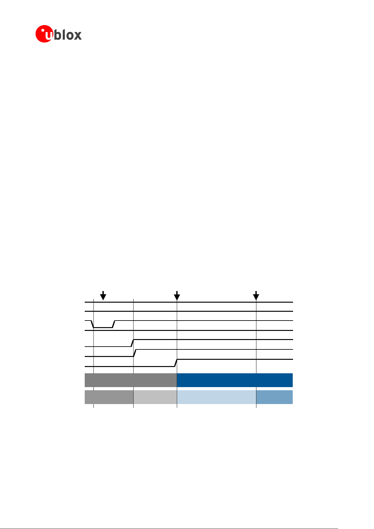
SARA-G3 and SARA-U2 series - System Integration Manual
VCC
V_BCKP
PWR_ON
SARA-U2 RESET_N
V_INT
SARA-G3 RESET_N
Internal Reset
System State
Digital Pins State
Internal Reset → Operational Operationa l
Tristate / Floating
OFF
ON
Internal Reset
Start of interface
configuration
Module interfaces
are configured
Start-up
event
1.6.1.3 Switch-on sequence from power-off mode
Figure 22 shows the modules power-on sequence from the power-off mode, describing the following phases:
The external supply is still applied to the VCC inputs as it is assumed that the module has been previously
switched off by means of the AT+CPWROFF command: the V_BCKP output is internally enabled as proper
VCC is present, the RESET_N of SARA-U2 series is set to high logic level due to internal pull-up to V_BCKP,
the PWR_ON is set to high logic level due to external pull-up connected to V_BCKP or VCC.
The PWR_ON input pin is set low for a valid time period, representing the start-up event.
All the generic digital pins of the modules are tri-stated until the switch-on of their supply source (V_INT):
any external signal connected to the generic digital pins must be tri-stated or set low at least until the
activation of the V_INT supply output to avoid latch-up of circuits and allow a proper boot of the module.
The V_INT generic digital interfaces supply output is enabled by the integrated power management unit.
The RESET_N line of SARA-G3 series rises suddenly to high logic level due to internal pull-up to V_INT.
The internal reset signal is held low by the integrated power management unit: the baseband processor core
and all the digital pins of the modules are held in reset state.
When the internal reset signal is released by the integrated power management unit, any digital pin is set in
a proper sequence from the reset state to the default operational state. The duration of this pin’s
configuration phase differs between the generic digital interfaces and the USB interface, due to specific
host / device enumeration timings (see section 1.9.3)
o Generic digital interfaces pin configuration time: 3 seconds typical on SARA-G3 and SARA-U2 series
modules, except for on SARA-U201 modules, which have 4 seconds typical
o USB interface configuration time: 5 seconds typical on SARA-G3 and SARA-U2 series modules, except
for on SARA-U201 modules, which have 6 seconds typical
The module is fully ready to operate after all the interfaces are configured.
Figure 22: SARA-G3 and SARA-U2 series power-on sequence from power-off mode
UBX-13000995 - R26 System description
Page 37 of 217
Page 38

SARA-G3 and SARA-U2 series - System Integration Manual
1.6.1.4 General considerations for the switch-on procedure
A greeting text can be activated by means of the +CSGT AT command (see the u-blox AT Commands Manual
[3]) to notify the external application that the module is ready to operate (i.e. ready to reply to AT commands)
and that the first AT command can be sent to the module. In this case, the UART autobauding must be disabled
to let the module send the greeting text: the UART must be configured at fixed baud rate (the baud rate of the
application processor) instead of the default autobauding, otherwise the module does not know the baud rate
to be used for sending the greeting text (or any other URC) at the end of the internal boot sequence.
As an alternative starting procedure, after the interfaces’ configuration phase, the application can start sending
AT commands and wait for the response with a 30 second timeout; iterate it 4 times without resetting or
removing the VCC supply of the module, and then run the application.
The Internal Reset signal is not available on a module pin, but the host application can monitor:
o The V_INT pin to sense the start of the module power-on sequence.
o The USB interface to sense the start of the SARA-U2 modules power-on sequence: the module, as a
USB device, informs the host of the attach event via a reply on its status change pipe for proper bus
enumeration process according to the Universal Serial Bus Revision 2.0 specification [14].
Before the switch-on of the generic digital interface supply source (V_INT) of the module, no voltage
driven by an external application should be applied to any generic digital interface of the module.
Before the modules are fully ready to operate, the host application processor should not send any AT
command over the AT communication module interfaces (USB, UART).
The duration of SARA-G3 and SARA-U2 series modules’ switch-on routine can vary depending on the
application / network settings and the concurrent module activities.
UBX-13000995 - R26 System description
Page 38 of 217
Page 39

SARA-G3 and SARA-U2 series - System Integration Manual
1.6.2 Module power-off
1.6.2.1 Switch-off events
The SARA-G3 and SARA-U2 series modules can be properly switched off by:
AT+CPWROFF command (more details in the u-blox AT Commands Manual [3]).
The SARA-U2 series modules can be properly switched off also by:
Low pulse on the PWR_ON pin, which is normally set high by an external pull-up, for a valid time period
(see the SARA-U2 series Data Sheet [2] for the detailed electrical characteristics of the PWR_ON input).
In both the cases listed above, the current parameter settings are saved in the module’s non-volatile memory and
a proper network detach is performed: these are the correct ways to switch off the modules.
An abrupt under-voltage shutdown occurs on SARA-G3 and SARA-U2 series modules when the VCC module
supply is removed, but in this case the current parameter settings are not saved in the module’s non-volatile
memory and a proper network detach cannot be performed.
It is highly recommended to avoid an abrupt removal of VCC supply during the modules’ normal
operations: the power-off procedure must be properly started by the application, as by the AT+CPWROFF
command, waiting the command response for a proper time period (see the u-blox AT Commands
Manual [3]), and then a proper VCC supply must be held at least until the end of the modules’ internal
power-off sequence, which occurs when the generic digital interfaces supply output (V_INT) is switched
off by the module.
An abrupt hardware shutdown occurs on SARA-U2 modules when a low level is applied to the RESET_N input.
In this case, the current parameter settings are not saved in the module’s non-volatile memory and a proper
network detach is not performed.
It is highly recommended to avoid an abrupt hardware shutdown of the module by forcing a low level on
the RESET_N input pin during module normal operation: the RESET_N line should be set low only if reset
or shutdown via AT commands fails or if the module does not reply to a specific AT command after a time
period longer than the one defined in the u-blox AT Commands Manual [3].
An over-temperature or an under-temperature shutdown occurs on SARA-G3 and SARA-U2 series modules
when the temperature measured within the cellular module reaches the dangerous area, if the optional Smart
Temperature Supervisor feature is enabled and configured by the dedicated AT command. For more details, see
section 1.13.10 and the u-blox AT Commands Manual [3], +USTS AT command.
The Smart Temperature Supervisor feature is not supported by SARA-G300 and SARA-G310.
UBX-13000995 - R26 System description
Page 39 of 217
Page 40

SARA-G3 and SARA-U2 series - System Integration Manual
VCC
V_BCKP
PWR_ON
SARA-U2 RESET_N
V_INT
SARA-G3 RESET_N
Internal Reset
System State
Digital Pins State Operational
OFF
Tristate / Floa ting
ON
Operational → Tristate
AT+CPWROFF
sent to the module
OK
replied by the module
VCC
can be removed
1.6.2.2 Switch-off sequence by AT+CPWROFF
Figure 23 describes the SARA-G3 and SARA-U2 series modules power-off sequence, properly started sending the
AT+CPWROFF command, allowing storage of the current parameter settings in the module’s non-volatile
memory and a proper network detach, with the following phases:
When the +CPWROFF AT command is sent, the module starts the switch-off routine.
The module replies OK on the AT interface: the switch-off routine is in progress.
At the end of the switch-off routine, all the digital pins are tri-stated and all the internal voltage regulators
are turned off, including the generic digital interfaces supply (V_INT), except the RTC supply (V_BCKP).
Then, the module remains in power-off mode as long as a switch-on event does not occur (e.g. applying a
proper low level to the PWR_ON input, or applying a proper low level to the RESET_N input), and enters
not-powered mode if the supply is removed from the VCC pins.
Figure 23: SARA-G3 and SARA-U2 series power-off sequence description
The Internal Reset signal is not available on a module pin, but the application can monitor the V_INT pin
The VCC supply can be removed only after the end of the module internal switch-off routine, i.e. only
The duration of each phase in the SARA-G3 and SARA-U2 series modules’ switch-off routines can largely
UBX-13000995 - R26 System description
Page 40 of 217
to sense the end of the SARA-G3 and SARA-U2 series power-off sequence.
after that the V_INT voltage level has gone low.
vary depending on the application / network settings and the concurrent module activities.
Page 41

SARA-G3 and SARA-U2 series - System Integration Manual
Baseband
Processor
18
RESET_N
SARA-U2 series
Reset
Power
Management
Reset
10k
V_BCKP
Baseband
Processor
18
RESET_N
SARA-G3 series
Reset
10k
V_INT
1.6.3 Module reset
SARA-G3 and SARA-U2 series modules can be properly reset (rebooted) by:
AT+CFUN command (see the u-blox AT Commands Manual [3] for more details).
This command causes an “internal” or “software” reset of the module, which is an asynchronous reset of the
module baseband processor. The current parameter settings are saved in the module’s non-volatile memory and
a proper network detach is performed: this is the proper way to reset the modules.
An abrupt hardware reset occurs on SARA-G3 and SARA-U2 series modules when a low level is applied on the
RESET_N input pin for a specific time period. In this case, the current parameter settings are not saved in the
module’s non-volatile memory and a proper network detach is not performed.
It is highly recommended to avoid an abrupt hardware reset of the module by forcing a low level on the
RESET_N input during modules normal operation: the RESET_N line should be set low only if reset or
shutdown via AT commands fails or if the module does not provide a reply to a specific AT command
after a time period longer than the one defined in the u-blox AT Commands Manual [3].
As described in Figure 24, both the SARA-G3 and SARA-U2 series modules are equipped with an internal pull-up
resistor which pulls the line to the high logic level when the RESET_N pin is not forced low from the external.
The pull-up is internally biased by V_INT on SARA-G3 modules and is biased by V_BCKP on SARA-U2 modules.
A series Schottky diode is mounted inside the SARA-G3 modules, increasing the RESET_N input voltage range.
See the SARA-G3 series Data Sheet [1] and the SARA-U2 series Data Sheet [2] for the detailed electrical
characteristics of the RESET_N input.
Figure 24: RESET_N input description
When a low level is applied to the RESET_N input, it causes an “external” or “hardware” reset of the modules,
with the following behavior of SARA-G3 and SARA-U2 series modules due to different internal circuits:
SARA-G3 modules: reset of the processor core, excluding the Power Management Unit and the RTC block.
The V_INT generic digital interfaces supply is switched on and each digital pin is set in its internal reset state.
The V_BCKP supply and the RTC block are switched on.
SARA-U2 modules: reset of the processor core and the Power Management Unit, excluding the RTC block.
The V_INT generic digital interfaces supply is switched off and all digital pins are tri-stated (not supplied).
The V_BCKP supply and the RTC block are switched on.
Before the switch-on of the generic digital interface supply source (V_INT) of the module, no voltage
driven by an external application should be applied to any generic digital interface of the modules.
The internal reset state of all digital pins is reported in the pin description table in the SARA-G3 series
Data Sheet [1] and in the SARA-U2 series Data Sheet [2].
UBX-13000995 - R26 System description
Page 41 of 217
Page 42

SARA-G3 and SARA-U2 series - System Integration Manual
1.6.4 External 32 kHz signal input (EXT32K)
The EXT32K pin is not available on SARA-G340, SARA-G350 and SARA-U2 series modules.
The EXT32K pin of SARA-G300 / SARA-G310 modules is an input pin that must be fed by a proper 32 kHz
signal to make available the reference clock for the Real Time Clock (RTC) timing, used by the module processor
when in the low power idle mode.
SARA-G300 / SARA-G310 modules can enter the low power idle mode only if a proper 32 kHz signal is provided
at the EXT32K input pin, with power saving configuration enabled by the AT+UPSV command. In this way the
different current consumption figures can be reached with the EXT32K input fed by the 32K_OUT output or by
a proper external 32 kHz signal (for more details, see section 1.5.1.4 and to “Current consumption” section in
the SARA-G3 series Data Sheet [1]).
SARA-G300 / SARA-G310 modules can provide the RTC functions (as RTC timing by AT+CCLK command and
RTC alarm by AT+CALA command) only if a proper 32 kHz signal is provided at the EXT32K input pin. The RTC
functions will be available only when the module is switched on if the EXT32K input is fed by the 32K_OUT
output, or they will be available also when the module is not powered or switched off if the EXT32K input is fed
by a proper external 32 kHz signal.
SARA-G3 series Data Sheet [1] describes the detailed electrical characteristics of the EXT32K input pin.
The 32 kHz reference clock for the RTC timing is automatically generated by the internal oscillator provided on
the SARA-G340, SARA-G350 and SARA-U2 series modules: the same pin (31) is a reserved (RSVD) pin internally
not connected, since an external 32 kHz signal is not needed to enter the low power idle mode and to provide
the RTC functions.
1.6.5 Internal 32 kHz signal output (32K_OUT)
The 32K_OUT pin is not available on SARA-G340, SARA-G350 and SARA-U2 series modules.
The 32K_OUT pin of SARA-G300 / SARA-G310 modules is an output pin that provides a 32 kHz reference signal
generated by the module, suitable only to feed the EXT32K input pin of SARA-G300 / SARA-G310 modules, to
make available the reference clock for the Real Time Clock (RTC) timing, so that the modules can enter the low
power idle mode and can provide the RTC functions with modules switched on.
The 32K_OUT pin does not provide the 32 kHz output signal when the SARA-G300 / SARA-G310 modules are
in power down mode: the EXT32K input pin must be fed by an external proper 32 kHz signal to make available
the RTC functions when the modules are not powered or switched off.
SARA-G340, SARA-G350 and SARA-U2 series modules do not provide the 32K_OUT output, as there is no
EXT32K input to feed on the modules: pin 24 constitutes the GPIO3 on these modules.
UBX-13000995 - R26 System description
Page 42 of 217
Page 43

SARA-G3 and SARA-U2 series - System Integration Manual
Item
Requirements
Remarks
Impedance
50 nominal characteristic impedance
The nominal characteristic impedance of the antenna RF
connection must match the ANT pin 50 impedance.
Frequency Range
See the SARA-G3 series Data Sheet [1] and the
SARA-U2 series Data Sheet [2]
The required frequency range of the antenna depends on
the operating bands supported by the cellular module.
Return Loss
S11 < -10 dB (VSWR < 2:1) recommended
S11 < -6 dB (VSWR < 3:1) acceptable
The Return loss or the S11, as the VSWR, refers to the
amount of reflected power, measuring how well the RF
antenna connection matches the 50 impedance.
The impedance of the antenna RF termination must match
as much as possible the 50 impedance of the ANT pin
over the operating frequency range, reducing as much as
possible the amount of reflected power.
Efficiency
> -1.5 dB ( > 70% ) recommended
> -3.0 dB ( > 50% ) acceptable
The radiation efficiency is the ratio of the radiated power
to the power delivered to antenna input: the efficiency is a
measure of how well an antenna receives or transmits.
The efficiency needs to be enough high over the operating
frequency range to comply with the Over-The-Air radiated
performance requirements, as Total Radiated Power and
Total Isotropic Sensitivity, specified by certification schemes
Maximum Gain
See section 4.2.2 for maximum gain limits
The power gain of an antenna is the radiation efficiency
multiplied by the directivity: the maximum gain describes
how much power is transmitted in the direction of peak
radiation to that of an isotropic source.
The maximum gain of the antenna connected to ANT pin
must not exceed the values stated in section 4.2.2 to
comply with regulatory agencies radiation exposure limits.
Input Power
> 2 W peak
The antenna connected to ANT pin must support the
maximum power transmitted by the modules.
Detection
Application board with antenna detection circuit
If antenna detection is required by the custom application,
proper antenna detection circuit must be implemented on
the application board as described in section 2.4.2.
Antenna assembly with built-in diagnostic circuit
If antenna detection is required by the custom application,
the external antenna assembly must be provided with
proper diagnostic circuit as described in section 2.4.2.
1.7 Antenna interface
1.7.1 Antenna RF interface (ANT)
The ANT pin of SARA-G3 and SARA-U2 series modules represents the RF input/output for 2G or 3G cellular RF
signals reception and transmission. The ANT pin has a nominal characteristic impedance of 50 and must be
connected to the antenna through a 50 transmission line for proper RF signals reception and transmission.
1.7.1.1 Antenna RF interface requirements
Table 9 summarizes the requirements for the antenna RF interface (ANT). See section 2.4.1 for suggestions to
properly design an antenna circuit compliant to these requirements.
The antenna circuit affects the RF compliance of the device integrating SARA-G3 and SARA-U2
series module with applicable required certification schemes. Compliance is guaranteed if the
antenna RF interface (ANT) requirements summarized in Table 9 are fulfilled.
Table 9: Summary of antenna RF interface (ANT) requirements
For the additional specific requirements applicable to the integration of SARA-G340 ATEX, SARA-G350
ATEX, SARA-U201 ATEX and SARA-U270 ATEX modules in applications intended for use in potentially
explosive atmospheres, see section 2.14.
UBX-13000995 - R26 System description
Page 43 of 217
Page 44

SARA-G3 and SARA-U2 series - System Integration Manual
1.7.2 Antenna detection interface (ANT_DET)
Antenna detection interface (ANT_DET) is not supported by SARA-G300 and SARA-G310 modules.
The antenna detection is based on ADC measurement. The ANT_DET pin is an Analog to Digital Converter
(ADC) provided to sense the antenna presence.
The antenna detection function provided by ANT_DET pin is an optional feature that can be implemented if the
application requires it. The antenna detection is forced by the +UANTR AT command. See the u-blox AT
Commands Manual [3] for more details on this feature.
The ANT_DET pin generates a DC current (20 µA for 5.4 ms on SARA-G340 / SARA-G350, 10 µA for 128 µs on
SARA-U2 modules) and measures the resulting DC voltage, thus determining the resistance from the antenna
connector provided on the application board to GND. So, the requirements to achieve antenna detection
functionality are the following:
an RF antenna assembly with a built-in resistor (diagnostic circuit) must be used
an antenna detection circuit must be implemented on the application board
See section 2.4.2 for design-in guidelines for antenna detection circuits on an application board and diagnostic
circuits on an antenna assembly.
1.8 SIM interface
1.8.1 (U)SIM card interface
SARA-G3 and SARA-U2 series modules provide a high-speed SIM/ME interface, including automatic detection
and configuration of the voltage required by the connected (U)SIM card or chip.
Both 1.8 V and 3 V SIM types are supported: activation and deactivation with automatic voltage switch from
1.8 V to 3 V is implemented, according to ISO-IEC 7816-3 specifications. The VSIM supply output pin provides
internal short circuit protection to limit start-up current and protect the device in short circuit situations.
The SIM driver supports the PPS (Protocol and Parameter Selection) procedure for baud-rate selection, according
to the values determined by the SIM Card.
The SIM Application Toolkit is supported by all SARA-G3 and SARA-U2 series except SARA-G300 and
SARA-G310.
1.8.2 SIM card detection interface (SIM_DET)
Not supported by SARA-G300-00S and SARA-G310-00S modules.
The SIM_DET pin is configured as an external interrupt to detect the SIM card mechanical / physical presence.
The pin is configured as input with an internal active pull-down enabled, and it can sense SIM card presence only
if properly connected to the mechanical switch of a SIM card holder as described in section 2.5:
Low logic level at SIM_DET input pin is recognized as SIM card not present
High logic level at SIM_DET input pin is recognized as SIM card present
The SIM card detection function provided by SIM_DET pin is an optional feature that can be implemented / used
or not according to the application requirements: an Unsolicited Result Code (URC) can be generated each time
that there is a change of status (for more details, see the “simind” value of the <descr> parameter of +CIND and
+CMER commands in the u-blox AT Commands Manual [3]).
The optional function “SIM card hot insertion/removal” can be additionally enabled on the SARA-U2 modules’
SIM_DET pin by AT commands (see the section 1.11 and the u-blox AT Commands Manual [3], +UGPIOC,
+UDCONF=50).
UBX-13000995 - R26 System description
Page 44 of 217
Page 45

SARA-G3 and SARA-U2 series - System Integration Manual
1.9 Serial interfaces
SARA-G3 and SARA-U2 series modules provide the following serial communication interfaces:
UART interface: 9-wire unbalanced 1.8 V asynchronous serial interface supporting (see 1.9.1)
o AT command mode
o Data mode and Online command mode
o MUX functionality, including dedicated GNSS tunneling
o FW upgrades by means of the FOAT feature
o FW upgrades by means of the u-blox EasyFlash tool
o Trace log capture (diagnostic purposes)
Auxiliary UART interface
o AT command mode
o GNSS tunneling
o FW upgrades by means of the u-blox EasyFlash tool
o Trace log capture (diagnostic purposes)
USB interface
25
: High-Speed USB 2.0 compliant interface supporting (see 1.9.3)
o AT command mode
o Data mode and Online command mode
o GNSS tunneling and SIM Access Profile virtual channels
o Ethernet-over-USB
o FW upgrades by means of the FOAT feature
o FW upgrades by means of the u-blox EasyFlash tool
o Trace log capture (diagnostic purposes)
DDC interface
27
: I2C-bus compatible 1.8 V interface supporting (see 1.9.4)
o Communication with u-blox GNSS positioning chips / modules
o Communication with other external I
17
21
: 3-wire unbalanced 1.8 V asynchronous serial interface supporting (see 1.9.2)
22
23
26
virtual channel
17
20
17
2
C devices as an audio codec28
18
and SIM Access Profile19 virtual channels
20
24
17
See the u-blox AT Commands Manual [3] for the definition of the command mode, data mode, and online command mode.
18
SARA-G300 and SARA-G310 modules do not support GNSS tunneling.
19
SARA-G3 modules do not support a SIM Access Profile.
20
SARA-G3 modules do not support FW upgrades using the u-blox EasyFlash tool and trace log capture over the UART.
21
SARA-U2 modules product versions “00”, “03”, “53”, “63”, “73” do not provide Auxiliary UART.
22
SARA-G3 modules product versions “00” and “01” do not support AT command mode over the Auxiliary UART.
23
SARA-G3 modules product versions “00” and “01”, and SARA-U2 modules do not support GNSS tunneling over the Auxiliary UART.
24
SARA-U2 modules do not support FW upgrades using the u-blox EasyFlash tool over the Auxiliary UART.
25
SARA-G3 modules do not provide a USB interface.
26
SARA-U2 modules product versions “00”do not support Ethernet-over-USB.
27
SARA-G300 and SARA-G310 modules do not support a DDC I2C-bus compatible interface.
28
SARA-G3 modules do not support communication with external I2C devices other than u-blox GNSS positioning chips / modules.
UBX-13000995 - R26 System description
Page 45 of 217
Page 46

SARA-G3 and SARA-U2 series - System Integration Manual
1.9.1 Asynchronous serial interface (UART)
1.9.1.1 UART features
The UART interface is a 9-wire 1.8 V unbalanced asynchronous serial interface available on all the SARA-G3 and
SARA-U2 series modules, supporting:
AT command mode
Data mode and Online command mode
29
29
Multiplexer protocol functionality (see 1.9.1.5)
FW upgrades by means of the FOAT feature (see 1.13.17)
FW upgrades by means of the u-blox EasyFlash tool (see the Firmware update application note [27])
Trace log capture (diagnostic purposes)
SARA-G3 modules do not support FW upgrades using the EasyFlash tool and trace log capture over UART.
SARA-G3 and SARA-U2 series modules’ UART interface is by default configured in AT command mode: the
module waits for AT command instructions and interprets all the characters received as commands to execute.
All the functionalities supported by SARA-G3 and SARA-U2 series modules can be in general set and configured
by AT commands (see the u-blox AT Commands Manual [3]).
The UART interface provides RS-232 functionality conforming to the ITU-T V.24 Recommendation (more details
available in ITU Recommendation [10]), with CMOS compatible signal levels: 0 V for low data bit or ON state,
and 1.8 V for high data bit or OFF state. For detailed electrical characteristics, see the SARA-G3 series Data
Sheet [1] and the SARA-U2 series Data Sheet [2].
SARA-G3 and SARA-U2 series modules are designed to operate as a 2G or 3G cellular modem, which represents
the Data Circuit-terminating Equipment (DCE) according to ITU-T V.24 Recommendation [10]. The application
processor connected to the module through the UART interface represents the Data Terminal Equipment (DTE).
The signal names of SARA-G3 and SARA-U2 series modules’ UART interface conform to the ITU-T V.24
Recommendation [10]: e.g. the TXD line represents the data transmitted by the DTE (application
processor data line output) and received by the DCE (module data line input).
All flow control handshakes are supported by the UART interface and can be set by appropriate AT commands
(see the u-blox AT Commands Manual [3], &K, +IFC, \Q AT commands): hardware, software, or none flow
control.
Hardware flow control is enabled by default.
SARA-G3 modules support the autobauding: the baud rate automatic detection is performed each time the DTE
sends AT commands. After the detection the module works at the detected baud rate and the baud rate can be
runtime changed by the DTE or by AT command (see the u-blox AT Commands Manual [3], +IPR command).
SARA-U2 modules support only the one-shot autobauding: the baud rate automatic detection is performed only
once, at module start-up. After the detection the module works at the detected baud rate and the baud rate can
only be changed by AT command (see the u-blox AT Commands Manual [3], +IPR command).
29
See the u-blox AT Commands Manual [3] for the definition of the command mode, data mode, and online command mode.
UBX-13000995 - R26 System description
Page 46 of 217
Page 47

SARA-G3 and SARA-U2 series - System Integration Manual
SARA-G3 modules’ autobauding and SARA-U2 modules’ one-shot autobauding are enabled by default.
The following baud rates can be configured by AT command (see the u-blox AT Commands Manual [3], +IPR):
1200 bit/s
2400 bit/s
4800 bit/s
9600 bit/s
19200 bit/s
38400 bit/s
57600 bit/s
115200 bit/s, default value when the autobauding or the one-shot autobauding are disabled
230400 bit/s
460800 bit/s
921600 bit/s
1200 bit/s, 230400 bit/s, 460800 bit/s and 921600 bit/s baud rates are not supported by SARA-G3
modules.
460800 bit/s and 921600 bit/s baud rates cannot be automatically detected by SARA-U2 modules.
SARA-G3 modules support the automatic frame recognition in conjunction with autobauding.
SARA-U2 modules support the one-shot automatic frame recognition in conjunction with one-shot autobauding.
SARA-G3 series modules’ automatic frame recognition and SARA-U2 series modules’ one-shot automatic
frame recognition are enabled by default, as autobauding and one-shot autobauding.
The following frame formats can be configured by AT command (see the u-blox AT Commands Manual [3],
+ICF):
8N1 (8 data bits, no parity, 1 stop bit), default frame configuration with fixed baud rate
8E1 (8 data bits, even parity, 1 stop bit)
8O1 (8 data bits, odd parity, 1 stop bit)
8N2 (8 data bits, no parity, 2 stop bits)
7E1 (7 data bits, even parity, 1 stop bit)
7O1 (7 data bits, odd parity, 1 stop bit)
Figure 25 describes the 8N1 frame format, which is the default configuration with fixed baud rate.
UBX-13000995 - R26 System description
Page 47 of 217
Page 48

SARA-G3 and SARA-U2 series - System Integration Manual
D0 D1 D2 D3 D4 D5 D6 D7
Start of 1-Byte
transfer
Start Bit
(Always 0)
Possible Start of
next transfer
Stop Bit
(Always 1)
t
bit
= 1/(Baudrate)
Normal Transfer, 8N1
Interface
AT Settings
Comments
UART interface
AT interface: enabled
AT command mode is enabled by default on the UART physical interface
AT+IPR=0
Automatic baud rate detection enabled by default on SARA-G3 series
One-shot automatic baud rate detection enabled by default on SARA-U2 series
AT+ICF=0
Automatic frame format recognition enabled by default on SARA-G3 series
One-shot automatic frame format recognition enabled by default on SARA-U2 series
AT&K3
HW flow control enabled by default
AT&S1
DSR line set ON in data mode30 and set OFF in command mode30
AT&D1
Upon an ON-to-OFF transition of DTR, the DCE enters online command mode30 and issues
an OK result code
AT&C1
Circuit 109 changes in accordance with the Carrier detect status; ON if the Carrier is
detected, OFF otherwise
MUX protocol: disabled
Multiplexing mode is disabled by default and it can be enabled by AT+CMUX command.
The following virtual channels are defined:
Channel 0: control channel
Channel 1: AT and data
Channel 2: AT and data
Channel 3: AT and data (not available on SARA-G300 / SARA-G310 modules)
Channel 4: AT and data (not available on SARA-G300 / SARA-G310 modules)
Channel 5: AT and data (not available on SARA-G300 / SARA-G310 modules)
Channel 6: GNSS tunneling (not available on SARA-G300 / SARA-G310 modules)
Channel 7: SIM Access Profile (not available on SARA-G3 series modules)
Figure 25: Description of UART default frame format (8N1) with fixed baud rate
The module firmware can be updated over the UART interface by means of:
the Firmware upgrade Over AT (FOAT) feature, on all the SARA-G3 and SARA-U2 series modules
the u-blox EasyFlash tool, on SARA-U2 series modules only
For more details on FW upgrade procedures see section 1.13 and Firmware update application note [27].
1.9.1.2 UART AT interface configuration
The UART interface of SARA-G3 and SARA-U2 series modules is available as AT command interface with the
default configuration described in Table 10 (for more details and information about further settings, see the
u-blox AT Commands Manual [3]).
Table 10: Default UART AT interface configuration
30
See the u-blox AT Commands Manual [3] for the definition of the command mode, data mode, and online command mode.
UBX-13000995 - R26 System description
Page 48 of 217
Page 49

SARA-G3 and SARA-U2 series - System Integration Manual
1.9.1.3 UART signal behavior
At the module switch-on, before the UART interface initialization (as described in the power-on sequence
reported in Figure 21 or Figure 22), each pin is first tri-stated and then is set to its related internal reset state31. At
the end of the boot sequence, the UART interface is initialized, the module is by default in active mode, and the
UART interface is enabled as AT commands interface.
The configuration and the behavior of the UART signals after the boot sequence are described below. See
section 1.4 for definition and description of module operating modes referred to in this section.
RXD signal behavior
The module data output line (RXD) is set by default to the OFF state (high level) at UART initialization. The
module holds RXD in the OFF state until the module does not transmit some data.
TXD signal behavior
The module data input line (TXD) is set by default to the OFF state (high level) at UART initialization. The TXD
line is then held by the module in the OFF state if the line is not activated by the DTE: an active pull-up is enabled
inside the module on the TXD input.
CTS signal behavior
The module hardware flow control output (CTS line) is set to the ON state (low level) at UART initialization.
If the hardware flow control is enabled, as it is by default, the CTS line indicates when the UART interface is
enabled (data can be sent and received). The module drives the CTS line to the ON state or to the OFF state
when it is either able or not able to accept data from the DTE over the UART (see 1.9.1.4 for more details).
If hardware flow control is enabled, then when the CTS line is OFF it does not necessarily mean that the
module is in low power idle mode, but only that the UART is not enabled, as the module could be forced
to stay in active mode for other activities, e.g. related to the network or related to other interfaces.
When the multiplexer protocol is active, the CTS line state is mapped to Fcon / Fcoff MUX command for
flow control issues outside the power saving configuration while the physical CTS line is still used as a
power state indicator. For more details, see Mux Implementation Application Note [25].
The CTS hardware flow control setting can be changed by AT commands (for more details, see the u-blox AT
Commands Manual [3], AT&K, AT\Q, AT+IFC, AT+UCTS AT command).
If the hardware flow control is not enabled, the CTS line after the UART initialization behaves as follows:
on SARA-U2 modules product version “00”, the CTS is always held in the ON state
on SARA-U2 modules product versions “x3” onwards, the CTS behaves as per AT+UCTS command setting
on SARA-G3 modules product versions “00” and “01”, the CTS is set in the ON or OFF state accordingly to
the power saving state as shown in Figure 28 if AT+UPSV=2 is set, and it is otherwise held in the ON state
on SARA-G3 modules product versions “02” onwards, the CTS behaves as per AT+UCTS command setting
When the power saving configuration is enabled and the hardware flow-control is not implemented in the
DTE/DCE connection, data sent by the DTE can be lost: the first character sent when the module is in the
low power idle mode will not be a valid communication character (see 1.9.1.4 for more details).
31
Refer to the pin description table in the SARA-G3 series Data Sheet [1] and SARA-U2 series Data Sheet [2].
UBX-13000995 - R26 System description
Page 49 of 217
Page 50

SARA-G3 and SARA-U2 series - System Integration Manual
RTS signal behavior
The hardware flow control input (RTS line) is set by default to the OFF state (high level) at UART initialization.
The module then holds the RTS line in the OFF state if the line is not activated by the DTE: an active pull-up is
enabled inside the module on the RTS input.
If the HW flow control is enabled, as it is by default, the module monitors the RTS line to detect permission from
the DTE to send data to the DTE itself. If the RTS line is set to the OFF state, any on-going data transmission
from the module is interrupted until the subsequent RTS line change to the ON state.
The DTE must still be able to accept a certain number of characters after the RTS line is set to the OFF
state: the module guarantees the transmission interruption within two characters from RTS state change.
Module behavior according to RTS hardware flow control status can be configured by AT commands (for more
details, see the u-blox AT Commands Manual [3], AT&K, AT\Q, AT+IFC command descriptions).
If AT+UPSV=2 is set and HW flow control is disabled, the module monitors the RTS line to manage the power
saving configuration:
When an OFF-to-ON transition occurs on the RTS input line, the UART is enabled and the module wakes up
to active mode: after ~20 ms from the OFF-to-ON transition the UART / module wake up is completed and
data can be received without loss. The module cannot enter the low power idle mode and the UART is kept
enabled as long as the RTS input line is held in the ON state
If the RTS input line is set to the OFF state by the DTE, the UART is disabled (held in low power mode) and
the module automatically enters low power idle mode whenever possible
For more details, see the section 1.9.1.4 and the u-blox AT Commands Manual [3], AT+UPSV command.
DSR signal behavior
If AT&S1 is set, as it is by default, the DSR module output line is set by default to the OFF state (high level) at
UART initialization. The DSR line is then set to the OFF state when the module is in command mode or in online
command mode and is set to the ON state when the module is in data mode (see the u-blox AT Commands
Manual [3] for the definition of the interface data mode, command mode and online command mode).
If AT&S0 is set, the DSR module output line is set by default to the ON state (low level) at UART initialization and
is then always held in the ON state.
DTR signal behavior
The DTR module input line is set by default to the OFF state (high level) at UART initialization. The module then
holds the DTR line in the OFF state if the line is not activated by the DTE: an active pull-up is enabled inside the
module on the DTR input.
Module behavior according to DTR status can be changed by AT command (for more details, see the u-blox AT
Commands Manual [3], AT&D command description).
If AT+UPSV=3 is set, the DTR line is monitored by the module to manage the power saving configuration:
When an OFF-to-ON transition occurs on the DTR input line, the UART is enabled and the module wakes up
to active mode: after ~20 ms from the OFF-to-ON transition the UART / module wake up is completed and
data can be received without loss. The module cannot enter the low power idle mode and the UART is kept
enabled as long as the DTR input line is held in the ON state
If the DTR input line is set to the OFF state by the DTE, the UART is disabled (held in low power mode) and
the module automatically enters low power idle mode whenever possible
For more details, see the section 1.9.1.4 and the u-blox AT Commands Manual [3], AT+UPSV command.
AT+UPSV=3 power saving configuration control by the DTR input is not supported by SARA-G3 modules.
UBX-13000995 - R26 System description
Page 50 of 217
Page 51
SARA-G3 and SARA-U2 series - System Integration Manual
DCD signal behavior
If AT&C1 is set, as it is by default, the DCD module output line is set by default to the OFF state (high level) at
UART initialization. The module then sets the DCD line according to the carrier detect status: ON if the carrier is
detected, OFF otherwise. For voice calls, DCD is set to the ON state when the call is established. For a data call,
there are the following scenarios (see the u-blox AT Commands Manual [3] for the definition of the interface
data mode, command mode and online command mode):
Packet Switched Data call: Before activating the PPP protocol (data mode) a dial-up application must
provide the ATD*99***<context_number># to the module: with this command the module switches from
command mode to data mode and can accept PPP packets. The module sets the DCD line to the ON state,
then answers with a CONNECT to confirm the ATD*99 command. The DCD ON is not related to the context
activation but with the data mode
Circuit Switched Data call: To establish a data call, the DTE can send the ATD<number> command to the
module which sets an outgoing data call to a remote modem (or another data module). Data can be
transparent (non reliable) or non transparent (with the reliable RLP protocol). When the remote DCE accepts
the data call, the module DCD line is set to ON and the CONNECT <communication baudrate> string is
returned by the module. At this stage the DTE can send characters through the serial line to the data
module which sends them through the network to the remote DCE attached to a remote DTE
The DCD is set to ON during the execution of the +CMGS, +CMGW, +USOWR, +USODL AT commands
requiring input data from the DTE: the DCD line is set to the ON state as soon as the switch to binary/text
input mode is completed and the prompt is issued; DCD line is set to OFF as soon as the input mode is
interrupted or completed (for more details, see the u-blox AT Commands Manual [3]).
The DCD line is kept in the ON state, even during the online command mode, to indicate that the data
call is still established even if suspended, while if the module enters command mode, the DSR line is set to
the OFF state. For more details, see DSR signal behavior description.
For scenarios when the DCD line setting is requested for different reasons (e.g. SMS texting during online
command mode), the DCD line changes to guarantee the correct behavior for all the scenarios. For
instance, for SMS texting in online command mode, if the data call is released, the DCD line is kept to ON
till the SMS command execution is completed (even if the data call release would request the DCD setting
to OFF).
If AT&C0 is set, the DCD module output line is set by default to the ON state (low level) at UART initialization
and is then always held in the ON state.
UBX-13000995 - R26 System description
Page 51 of 217
Page 52

SARA-G3 and SARA-U2 series - System Integration Manual
SMS arrives
time [s]
0
RI ON
RI OFF
1s
SMS
time [s]
0
RI ON
RI OFF
1s
1s
time [s]
151050
RI ON
RI OFF
Call incomes
1s
time [s]
151050
RI ON
RI OFF
Call incomes
RI signal behavior
The RI module output line is set by default to the OFF state (high level) at UART initialization. Then, during an
incoming call, the RI line is switched from the OFF state to the ON state with a 4:1 duty cycle and a 5 second
period (ON for 1 s, OFF for 4 s, see Figure 26), until the DTE attached to the module sends the ATA string and
the module accepts the incoming data call. The RING string sent by the module (DCE) to the serial port at
constant time intervals is not correlated with the switch of the RI line to the ON state.
Figure 26: RI behavior during an incoming call
The RI line can notify an SMS arrival. When the SMS arrives, the RI line switches from OFF to ON for 1 second
(see Figure 27), if the feature is enabled by the AT+CNMI command (see the u-blox AT Commands Manual [3]).
Figure 27: RI behavior at SMS arrival
This behavior allows the DTE to stay in power saving mode until the DCE related event requests service.
For SMS arrival, if several events coincidently occur or in quick succession each event independently triggers the
RI line, although the line will not be deactivated between each event. As a result, the RI line may stay to ON for
more than 1 s.
If an incoming call is answered within less than 1 second (with ATA or if auto-answering is set to ATS0=1) than
the RI line is set to OFF earlier.
As a result:
RI line monitoring cannot be used by the DTE to determine the number of received SMSes.
For multiple events (incoming call plus SMS received), the RI line cannot be used to discriminate the two
events, but the DTE must rely on the subsequent URCs and interrogate the DCE with proper commands.
The RI line can additionally notify all the URCs and all the incoming data (PPP, Direct Link, sockets, FTP), if the
feature is enabled by the AT+URING command (for more details, see the u-blox AT Commands Manual [3]): the
RI line is asserted when one of the configured events occur and it remains asserted for 1 second unless another
configured event will happen, with the same behavior described in Figure 27.
The AT+URING command for the notification of all the URCs and all the incoming data (PPP, Direct Link,
sockets, FTP) over the RI line output is not supported by SARA-G3 modules.
UBX-13000995 - R26 System description
Page 52 of 217
Page 53

SARA-G3 and SARA-U2 series - System Integration Manual
AT+UPSV
HW flow control
RTS line
DTR line
Communication during idle mode and wake up
0
Enabled (AT&K3)
ON
ON or OFF
Data sent by the DTE are correctly received by the module.
Data sent by the module is correctly received by the DTE.
0
Enabled (AT&K3)
OFF
ON or OFF
Data sent by the DTE should be buffered by the DTE and will be correctly
received by the module when RTS is set to ON.
Data sent by the module is buffered by the module and will be correctly
received by the DTE when it is ready to receive data (i.e. RTS line will be ON).
0
Disabled (AT&K0)
ON or OFF
ON or OFF
Data sent by the DTE is correctly received by the module.
Data sent by the module is correctly received by the DTE if it is ready to receive
data, otherwise data is lost.
1
Enabled (AT&K3)
ON
ON or OFF
Data sent by the DTE should be buffered by the DTE and will be correctly
received by the module when active mode is entered.
Data sent by the module is correctly received by the DTE.
1
Enabled (AT&K3)
OFF
ON or OFF
Data sent by the DTE should be buffered by the DTE and will be correctly
received by the module when active mode is entered.
Data sent by the module is buffered by the module and will be correctly
received by the DTE when it is ready to receive data (i.e. RTS line will be ON).
1
Disabled (AT&K0)
ON or OFF
ON or OFF
The first character sent by the DTE is lost, but after ~20 ms the UART and the
module are waked up: recognition of subsequent characters is guaranteed after
the complete UART / module wake-up.
Data sent by the module is correctly received by the DTE if it is ready to receive
data, otherwise data is lost.
2
Enabled (AT&K3)
ON or OFF
ON or OFF
Not Applicable: HW flow control cannot be enabled with AT+UPSV=2.
2
Disabled (AT&K0)
ON
ON or OFF
Data sent by the DTE is correctly received by the module.
Data sent by the module is correctly received by the DTE if it is ready to receive
data, otherwise data is lost.
2
Disabled (AT&K0)
OFF
ON or OFF
Data sent by the DTE is lost by SARA-U2 modules.
The first character sent by the DTE is lost by SARA-G3 modules, but after
~20 ms the UART and the module are waked up: recognition of subsequent
characters is guaranteed after the complete UART / module wake-up.
Data sent by the module is correctly received by the DTE if it is ready to receive
data, otherwise data is lost.
1.9.1.4 UART and power-saving
The power saving configuration is controlled by the AT+UPSV command (for the complete description, see the
u-blox AT Commands Manual [3]). When power saving is enabled, the module automatically enters low power
idle mode whenever possible, and otherwise the active mode is maintained by the module (see section 1.4 for
definition and description of module operating modes referred to in this section).
The AT+UPSV command configures both the module power saving and also the UART behavior in relation to the
power saving. The conditions for the module entering idle mode also depend on the UART power saving
configuration.
Three different power saving configurations can be set by the AT+UPSV command:
AT+UPSV=0, power saving disabled: module forced on active mode and UART interface enabled (default)
AT+UPSV=1, power saving enabled: module cyclic active / idle mode and UART enabled / disabled
AT+UPSV=2, power saving enabled and controlled by the UART RTS input line
AT+UPSV=3, power saving enabled and controlled by the UART DTR input line
The AT+UPSV=3 power saving configuration is not supported by SARA-G3 modules.
The different power saving configurations that can be set by the +UPSV AT command are described in details in
the following subsections. Table 11 summarizes the UART interface communication process in the different
power saving configurations, in relation with HW flow control settings and RTS input line status. For more
details on the +UPSV AT command description, refer to the u-blox AT commands Manual [3].
UBX-13000995 - R26 System description
Page 53 of 217
Page 54

SARA-G3 and SARA-U2 series - System Integration Manual
AT+UPSV
HW flow control
RTS line
DTR line
Communication during idle mode and wake up
3
Enabled (AT&K3)
ON
ON
Data sent by the DTE is correctly received by the module.
Data sent by the module is correctly received by the DTE.
3
Enabled (AT&K3)
ON
OFF
Data sent by the DTE is lost by the module.
Data sent by the module is correctly received by the DTE.
3
Enabled (AT&K3)
OFF
ON
Data sent by the DTE is correctly received by the module.
Data sent by the module is buffered by the module and will be correctly
received by the DTE when it is ready to receive data (i.e. RTS line will be ON).
3
Enabled (AT&K3)
OFF
OFF
Data sent by the DTE is lost by the module.
Data sent by the module is buffered by the module and will be correctly
received by the DTE when it is ready to receive data (i.e. RTS line will be ON).
3
Disabled (AT&K0)
ON or OFF
ON
Data sent by the DTE is correctly received by the module.
Data sent by the module is correctly received by the DTE if it is ready to receive
data, otherwise data are lost.
3
Disabled (AT&K0)
ON or OFF
OFF
Data sent by the DTE is lost by the module.
Data sent by the module is correctly received by the DTE if it is ready to receive
data, otherwise data are lost.
Table 11: UART and power-saving summary
AT+UPSV=0: power saving disabled, fixed active mode
The module does not enter idle mode and the UART interface is enabled (data can be sent and received): the
CTS line is always held in the ON state after UART initialization. This is the default configuration.
AT+UPSV=1: power saving enabled, cyclic idle/active mode
On SARA-G3 modules, when the AT+UPSV=1 command is issued by the DTE, the UART is disabled after the
timeout set by the second parameter of the +UPSV AT command (for more details, see the u-blox AT commands
Manual [3]).
On SARA-U2 modules, when the AT+UPSV=1 command is issued by the DTE, the UART is immediately disabled.
Afterwards, the UART of SARA-G3 and SARA-U2 series modules is periodically enabled to receive or send data
and, if data has not been received or sent over the UART, the interface is automatically disabled whenever
possible according to the timeout configured by the second parameter of the +UPSV AT command.
The module automatically enters the low power idle mode whenever possible but it wakes up to active mode
according to the UART periodic wake up so that the module cyclically enters the low power idle mode and the
active mode. Additionally, the module wakes up to active mode according to any required activity related to the
network or any other required activity related to the functions / interfaces of the module.
The UART is enabled, and the module does not enter low power idle mode, in the following cases:
During the periodic UART wake up to receive or send data
If the module needs to transmit some data over the UART (e.g. URC)
On SARA-G3 modules, during a CSD data call and a PSD data call with external context activation
On SARA-G3 modules, during a voice call
If a character is sent by the DTE with HW flow control disabled, the first character sent causes the system
wake-up due to the “wake up via data reception” feature described in the following subsection, and the
UART will be then kept enabled after the last data received according to the timeout set by the second
parameter of the AT+UPSV=1 command
The module, outside an active call, periodically wakes up from idle mode to active mode to monitor the paging
channel of the current base station (paging block reception), according to 2G or 3G discontinuous reception
(DRX) specification.
UBX-13000995 - R26 System description
Page 54 of 217
Page 55

SARA-G3 and SARA-U2 series - System Integration Manual
time [s]
CTS ON
CTS OFF
UART disabled
~10 ms (min)
UART enabled
~9.2 s (default)
UART enabled
Data input
0.47- 2.10 s
The time period between two paging receptions is defined by the current base station (i.e. by the network):
If the module is registered with a 2G network, the paging reception period can vary from ~0.47 s (DRX = 2,
i.e. 2 x 51 2G-frames) up to ~2.12 s (DRX = 9, i.e. 9 x 51 2G-frames)
If the module is registered with a 3G network, the paging reception period can vary from 0.64 s (DRX = 6,
i.e. 26 3G-frames) up to 5.12 s (DRX = 9, i.e. 29 3G-frames)
The time period of the UART enable/disable cycle is configured differently when the module is registered with a
2G network compared to when the module is registered with a 3G network:
2G: the UART is synchronously enabled to every paging reception on SARA-G3 modules, whereas the UART
is not necessarily enabled at every paging reception on SARA-U2 modules: the UART is enabled concurrently
to a paging reception, and then, as data has not been received or sent, the UART is disabled until the first
paging reception that occurs after a timeout of 2.0 s, and therefore the interface is enabled again
3G: the UART is asynchronously enabled to paging receptions, as the UART is enabled for ~20 ms, and then,
if data are not received or sent, the UART is disabled for 2.5 s, and afterwards the interface is enabled again
Not registered: when a module is not registered with a network, the UART is enabled for ~20 ms, and then,
if data has not been received or sent, the UART is disabled for ~2.1 s on SARA-G3 modules or for 2.5 s on
SARA-U2 modules, and afterwards the interface is enabled again
The module active mode duration outside an active call depends on:
Network parameters, related to the time interval for the paging block reception (minimum of ~11 ms)
Duration of UART enable time in absence of data reception (~20 ms)
The time period from the last data received at the serial port during the active mode: the module does not
enter idle mode until a timeout expires. The second parameter of the +UPSV AT command configures this
timeout, from 40 2G-frames (i.e. 40 x 4.615 ms = 184 ms) up to 65000 2G-frames (i.e. 65000 x 4.615 ms =
300 s). Default value is 2000 2G-frames (i.e. 2000 x 4.615 ms = 9.2 s)
The active mode duration can be extended indefinitely since every subsequent character received during the
active mode, resets and restarts the timer.
The timeout is ignored only by SARA-U2 modules immediately after AT+UPSV=1 has been sent, so that the
UART interface is disabled and the module may enter idle mode immediately after the AT+UPSV=1 is sent
The hardware flow-control output (CTS line) indicates when the UART interface is enabled (data can be sent and
received over the UART), if HW flow control is enabled, as illustrated in Figure 28.
Figure 28: CTS behavior with power saving enabled (AT+UPSV=1) and HW flow control enabled: the CTS output line indicates
when the UART interface of the module is enabled (CTS = ON = low level) or disabled (CTS = OFF = high level)
UBX-13000995 - R26 System description
Page 55 of 217
Page 56

SARA-G3 and SARA-U2 series - System Integration Manual
AT+UPSV=2: power saving enabled and controlled by the RTS line
This configuration can only be enabled with the module hardware flow control disabled by AT&K0 command.
The UART interface is immediately disabled after the DTE sets the RTS line to OFF.
Then, the module automatically enters idle mode whenever possible according to any required activity related to
the network or any other required activity related to the functions / interfaces of the module.
The UART is disabled as long as the RTS line is held to OFF, but the UART is enabled in the following cases:
If the module needs to transmit some data over the UART (e.g. URC)
On SARA-G3 modules, during a CSD data call and a PSD data call with external context activation
On SARA-G3 modules, during a voice call
On SARA-G3 modules, if a data is sent by the DTE, it causes the system wake-up due to the “wake up via
data reception” feature described in the following subsection, and the UART will be then kept enabled after
the last data received according to the timeout previously set with the AT+UPSV=1 configuration
When an OFF-to-ON transition occurs on the RTS input line, the UART is re-enabled and the module, if it was in
idle mode, switches from idle to active mode after ~20 ms: this is the UART and module “wake up time”.
If the RTS line is set to ON by the DTE the module is not allowed to enter the low power idle mode and the
UART is kept enabled.
On SARA-G3 modules product versions “00” and “01”, the CTS output line indicates the power saving
state as illustrated in Figure 28, even with AT+UPSV=2, while the CTS output line follows the AT+UCTS
command setting on product versions “02” onwards.
AT+UPSV=3: power saving enabled and controlled by the DTR line
The AT+UPSV=3 power saving configuration is not supported by SARA-G3 modules.
The AT+UPSV=3 configuration can be enabled regardless of the flow control setting on UART. In particular, the
HW flow control can be enabled (AT&K3) or disabled (AT&K0) on UART during this configuration.
The UART interface is immediately disabled after the DTE sets the DTR line to OFF.
Then, the module automatically enters idle mode whenever possible according to any required activity related to
the network or any other required activity related to the functions / interfaces of the module.
The UART is disabled as long as the DTR line is set to OFF, but the UART is enabled in case the module needs to
transmit some data over the UART (e.g. URC).
When an OFF-to-ON transition occurs on the DTR input line, the UART is re-enabled and the module, if it was in
idle mode, switches from idle to active mode after 20 ms: this is the UART and module “wake up time”.
If the DTR line is set to ON by the DTE, the module is not allowed to enter idle mode and the UART is kept
enabled until the DTR line is set to OFF.
When the AT+UPSV=3 configuration is enabled, the DTR input line can still be used by the DTE to control the
module behavior according to AT&D command configuration (see the u-blox AT Commands Manual [3]).
The CTS output line indicates the UART power saving state as illustrated in Figure 28, if HW flow control
is enabled with AT+UPSV=3.
UBX-13000995 - R26 System description
Page 56 of 217
Page 57

SARA-G3 and SARA-U2 series - System Integration Manual
OFF
ON
DCE UART is enabled for 2000 GSM frames (~9.2 s)
time
Wake up time: ~20 ms
time
TXD input
Wake up character
Not recognized by DCE
UART
OFF
ON
Wake up via data reception
The UART wake up via data reception consists of a special configuration of the module TXD input line that
causes the system wake-up when a low-to-high transition occurs on the TXD input line. In particular, the UART
is enabled and the module switches from the low power idle mode to active mode within ~20 ms from the first
character received: this is the system “wake up time”.
As a consequence, the first character sent by the DTE when the UART is disabled (i.e. the wake up character) is
not a valid communication character even if the wake up via data reception configuration is active, because it
cannot be recognized, and the recognition of the subsequent characters is guaranteed only after the complete
system wake-up (i.e. after ~20 ms).
The UART wake up via data reception configuration is active in the following cases:
On SARA-G3 series, the TXD input line is configured to wake up the system via data reception if:
o AT+UPSV=1 is set with HW flow control disabled
o AT+UPSV=2 is set with HW flow control disabled, and the RTS line is set OFF
On SARA-U2 series, the TXD input line is configured to wake up the system via data reception only if
o AT+UPSV=1 is set with hardware flow control disabled
On SARA-U2 series, the UART wake up via data reception configuration is not active on the TXD input,
and therefore all the data sent by the DTE is lost, if:
o AT+UPSV=2 is set with HW flow control disabled, and the RTS line is set OFF
o AT+UPSV=3 is set, regardless of the HW flow control setting, and the DTR line is set OFF
Figure 29 and Figure 30 show examples of common scenarios and timing constraints:
AT+UPSV=1 power saving configuration is active and the timeout from last data received to idle mode start
is set to 2000 frames (AT+UPSV=1,2000)
Hardware flow control is disabled
Figure 29 shows the case where the module UART is disabled and only a wake-up is forced. In this scenario the
only character sent by the DTE is the wake-up character; as a consequence, the DCE module UART is disabled
when the timeout from last data received expires (2000 frames without data reception, as the default case).
Figure 29: Wake-up via data reception without further communication
UBX-13000995 - R26 System description
Page 57 of 217
Page 58

SARA-G3 and SARA-U2 series - System Integration Manual
DCE UART is enabled for 2000 GSM frames (~9.2s)
after the last data received
time
Wake up time: ~20 ms
time
Wake up character
Not recognized by DCE
Valid characters
Recognized by DCE
OFF
ON
TXD input
UART
OFF
ON
Figure 30 shows the case where in addition to the wake-up character further (valid) characters are sent. The
wake up character wakes-up the module UART. The other characters must be sent after the “wake up time” of
~20 ms. If this condition is satisfied, the module (DCE) recognizes characters. The module will disable the UART
after 2000 GSM frames from the latest data reception.
Figure 30: Wake-up via data reception with further communication
The “wake-up via data reception” feature cannot be disabled.
In command mode
DTE must always send a character to the module before the “AT” prefix set at the beginning of each
command line: the first character is ignored if the module is in active mode, or it represents the wake-up
character if the module is in idle mode.
In command mode
command line: the first character is not ignored if the module is in active mode (i.e. the module replies
“OK”), or it represents the wake up character if the module is in low power idle mode (i.e. the module
does not reply).
32
, if autobauding is enabled and the DTE does not implement HW flow control, the
32
, if autobauding is disabled, the DTE must always send a dummy “AT” before each
No wake-up character or dummy “AT” is required from the DTE during a voice or data call since the
module UART interface continues to be enabled and does not need to be woken-up. Furthermore in data
mode32 a dummy “AT” would affect the data communication.
Additional considerations for SARA-U2 modules
SARA-U2 modules are forced to stay in active mode if the USB is connected and not suspended, and therefore
the AT+UPSV=1, AT+UPSV=2 or AT+UPSV=3 settings are overruled but they have effect on the UART behavior:
they configure UART interface power saving, so that UART is enabled / disabled according to the AT+UPSV=1,
AT+UPSV=2 or AT+UPSV=3 settings.
To set the AT+UPSV=1, AT+UPSV=2 or AT+UPSV=3 configuration over the USB interface of SARA-U2 modules,
the autobauding must be previously disabled on the UART by the +IPR AT command over the used AT interface
(the USB), and this +IPR AT command configuration must be saved in the module’ non-volatile memory (see the
u-blox AT Commands Manual [3]). Then, after the subsequent module re-boot, AT+UPSV=1, AT+UPSV=2 or
AT+UPSV=3 can be issued over the used AT interface (the USB): all the AT profiles are updated accordingly.
32
See the u-blox AT Commands Manual [3] for the definition of the command mode, data mode, and online command mode.
UBX-13000995 - R26 System description
Page 58 of 217
Page 59

SARA-G3 and SARA-U2 series - System Integration Manual
1.9.1.5 Multiplexer protocol (3GPP TS 27.010)
SARA-G3 and SARA-U2 series modules have a software layer with MUX functionality, the 3GPP TS 27.010
Multiplexer Protocol [13], available on the UART physical link. The auxiliary UART, the USB and the DDC (I2C)
serial interfaces do not support the multiplexer protocol.
This is a data link protocol (layer 2 of OSI model) which uses HDLC-like framing and operates between the
module (DCE) and the application processor (DTE) and allows a number of simultaneous sessions over the used
physical link (UART or SPI): the user can concurrently use AT command interface on one MUX channel and
Packet-Switched / Circuit-Switched Data communication on another multiplexer channel. Each session consists of
a stream of bytes transferring various kinds of data such as SMS, CBS, PSD, GNSS, AT commands in general. This
permits, for example, SMS to be transferred to the DTE when a data connection is in progress.
The following virtual channels are defined:
Channel 0: control channel
Channel 1: AT and data
Channel 2: AT and data
Channel 3: AT and data (not available on SARA-G300 / SARA-G310 modules)
Channel 4: AT and data (not available on SARA-G300 / SARA-G310 modules)
Channel 5: AT and data (not available on SARA-G300 / SARA-G310 modules)
Channel 6: GNSS tunneling (not available on SARA-G300 / SARA-G310 modules)
Channel 7: SIM Access Profile (not available on SARA-G3 series modules)
For more details, see the Mux implementation Application Note [25].
1.9.2 Auxiliary asynchronous serial interface (AUX UART)
The auxiliary UART interface is not available on SARA-U2 “00”, “03”, “53”, “63”, “73” product versions.
The auxiliary UART interface is a 3-wire 1.8 V unbalanced asynchronous serial interface available over:
RXD_AUX data output pin and TXD_AUX data input pin on SARA-G3 modules
SCL pin configured as RXD_AUX output and SDA pin configured as TXD_AUX input on SARA-U2 modules
The auxiliary UART interface supports:
AT command mode
33
GNSS tunneling mode
FW upgrades by means of the u-blox EasyFlash tool (see the Firmware update application note [27])
Trace log capture (diagnostic purposes)
SARA-G3 series modules product versions “00” and “01” do not support the AT command mode and the
GNSS tunneling mode over the Auxiliary UART interface.
SARA-U2 series modules do not support the GNSS tunneling and FW upgrades by means of the u-blox
EasyFlash tool over the Auxiliary UART interface.
SARA-G3 and SARA-U2 series modules do not support the Data mode and Online command mode
the Auxiliary UART interface.
33
over
33
See the u-blox AT Commands Manual [3] for the definition of the command mode, data mode, and online command mode.
UBX-13000995 - R26 System description
Page 59 of 217
Page 60

SARA-G3 and SARA-U2 series - System Integration Manual
AT+USIO
UART
AUX UART
I2S and GPIO3
Remarks
0
AT, Data and MUX
AT
Diagnostic
Digital audio and GPIO3 functionalities not available:
I2S_TXD, I2S_RXD, I2S_CLK, I2S_WA and GPIO3 pins
are configured for diagnostics as alternative function
1
AT, Data and MUX
Diagnostic
I2S and GPIO3
Default configuration
Digital audio and GPIO3 functionalities are available
2
AT, Data and MUX
AT
I2S and GPIO3
Digital audio and GPIO3 functionalities are available
3
AT, Data and MUX
GNSS tunneling
Diagnostic
Digital audio and GPIO3 functionalities not available:
I2S_TXD, I2S_RXD, I2S_CLK, I2S_WA and GPIO3 pins
are configured for diagnostics as alternative function
4
AT, Data and MUX
GNSS tunneling
I2S and GPIO3
Digital audio and GPIO3 functionalities are available
AT+USIO
UART
AUX UART
USB
Remarks
0
AT, Data and MUX
I2C
AT, Data, GNSS tunneling,
SAP, Ethernet-over-USB,
Diagnostic
Default configuration
DDC (I2C) interface functionalities are available
1
Diagnostic
I2C
AT, Data, GNSS tunneling,
SAP, Ethernet-over-USB
DDC (I2C) interface functionalities are available
2
Diagnostic
I2C
AT, Data, GNSS tunneling,
SAP, Ethernet-over-USB
DDC (I2C) interface functionalities are available
3
AT, Data and MUX
I2C
AT, Data, GNSS tunneling,
SAP, Ethernet-over-USB,
Diagnostic
DDC (I2C) interface functionalities are available
4
AT, Data and MUX
AT
AT, Data, GNSS tunneling,
SAP, Ethernet-over-USB,
Diagnostic
DDC (I2C) interface functionalities are not available:
DDC (I2C) interface’ pins are configured for Auxiliary
UART AT command mode, as alternative function
5
AT, Data and MUX
Diagnostic
AT, Data, GNSS tunneling,
SAP, Ethernet-over-USB
DDC (I2C) interface functionalities are not available:
DDC (I2C) interface’ pins are configured for Auxiliary
UART Diagnostic mode, as alternative function
6
Diagnostic
AT
AT, Data, GNSS tunneling,
SAP, Ethernet-over-USB
DDC (I2C) interface functionalities are not available:
DDC (I2C) interface’ pins are configured for Auxiliary
UART AT command mode, as alternative function
SARA-G3 modules’ auxiliary UART interface is by default configured for trace log capture (diagnostic purposes).
SARA-U2 modules’ auxiliary UART interface is by default configured as DDC (I2C) interface.
The serial interface configuration can be changed by means of the AT+USIO command to select different
alternative serial interface configuration variants, summarized in Table 12 and Table 13, available in a mutually
exclusive way (for more details, see the u-blox AT Commands Manual [3], +USIO AT command).
Table 12: Alternative serial interface configuration variants supported by SARA-G3 modules product versions “02” onwards
Table 13: Alternative serial interface configuration variants supported by SARA-U2 modules product versions “04” onwards
The serial interface configuration cannot be changed on the “00” and “01” product versions of the
SARA-G3 series modules, and on the “00” and “x3” product versions of the SARA-U2 series modules: the
AT+USIO command is not supported.
The serial interface configuration change triggered by means of the AT+USIO command, is not performed
run-time. The settings are saved in the Non-Volatile Memory at the module power off, and the new
configuration will be effective at the subsequent module reboot.
UBX-13000995 - R26 System description
Page 60 of 217
Page 61
SARA-G3 and SARA-U2 series - System Integration Manual
SARA-G3 and SARA-U2 series modules’ auxiliary UART interface can be configured in AT command mode by
means of the AT+USIO command (for more details, see Table 12 and Table 13), so that:
the cellular module waits for AT command instructions and interprets all the characters received over the
auxiliary UART interface as commands to execute
the auxiliary UART interface provides RS-232 functionality conforming to the ITU-T V.24 Recommendation
(more details available in ITU Recommendation [10]), with CMOS compatible signal levels: 0 V for low data
bit or ON state, and 1.8 V for high data bit or OFF state (for detailed electrical characteristics see the
SARA-G3 series Data Sheet [1] and the SARA-U2 series Data Sheet [2])
the cellular module is designed to operate as a modem, which represents the Data Circuit-terminating
Equipment (DCE) according to ITU-T V.24 Recommendation [10]: the application processor connected to the
module through the auxiliary UART interface represents the Data Terminal Equipment (DTE)
Software flow control and None flow control can be set (see the u-blox AT Commands Manual [3], &K,
+IFC, \Q AT commands), with default setting None flow control
1200, 2400, 4800, 9600, 19200, 38400, 57600, 115200, 230400, 460800 and 921600 bit/s baud rates can
be set (see the u-blox AT Commands Manual [3], +IPR)
8N1, 8N2, 8E1, 8O1, 7E1 or 7O1 frame format can be set (see the u-blox AT Commands Manual [3], +ICF)
The signal names of SARA-G3 series modules’ auxiliary UART interface conform to the ITU-T V.24
Recommendation [10]: e.g. the TXD_AUX line represents the data transmitted by the DTE (application
processor data line output) and received by the DCE (module data line input).
Hardware flow control is not supported on the auxiliary UART interface.
1200, 230400, 460800 and 921600 bit/s baud rates are not supported by SARA-G3 modules on the
auxiliary UART interface.
SARA-G3 modules do not support automatic baud rate detection (autobauding) and automatic frame
recognition on the auxiliary UART interface: 115200 bit/s and 8N1 are the default setting.
SARA-U2 modules support the one-shot automatic baud rate detection (one-shot autobauding) and the
one-shot automatic frame recognition, which are the default setting. The baud rate and frame automatic
detection is performed only once, at module start-up. After the detection, the module works at the
detected baud rate and frame format, and then they can only be changed by AT command (see the
u-blox AT Commands Manual [3], +IPR and +ICF command).
Data mode and Online command mode are not supported over the Auxiliary UART interface, so that for example
the ATD command for data call, the ATO command for online data state resuming, the AT+CGDATA command
for data state entering and the AT+USODL command for direct link are not supported, but Mobile Originated
voice call can be accepted, Mobile Terminated voice call can be triggered and voice call hang-up can be done
over the auxiliary UART interface.
The auxiliary UART interface provides only data output and input signals, so that for example the AT&C, AT&D
and AT&S commands have no effect on the interface, since there are no DCD, DTR and DSR lines available.
When the auxiliary UART interface is configured in AT command mode by means of the AT+USIO command (for
more details, see Table 12, Table 13 and the u-blox AT Commands Manual [3]), then both the UART and the
auxiliary UART interfaces can receive AT commands in parallel. The UART can be used for AT commands, data
communication and Multiplexer functionalities, while auxiliary UART can be used for AT commands only.
See the “Multiple AT command interfaces” appendix in the u-blox AT Commands Manual [3], for further details
regarding multiple AT command interfaces general usage and related AT command profile configurations.
The power saving configuration is controlled by the AT+UPSV command, which can be retrieved over the
auxiliary UART interface as over the UART interface: it sets the module power saving configuration and also the
interface behavior in relation to the power saving. For further details regarding power saving configurations, see
section 1.9.1.4 and the u-blox AT Commands Manual [3], +UPSV AT command.
UBX-13000995 - R26 System description
Page 61 of 217
Page 62

SARA-G3 and SARA-U2 series - System Integration Manual
The multiplexer protocol is not supported over SARA-G3 and SARA-U2 series modules’ Auxiliary UART interface.
SARA-G3 modules’ auxiliary UART interface can be configured in GNSS tunneling mode by means of the
AT+USIO command (for more details, see Table 12 and the u-blox AT Commands Manual [3]), so that:
raw data flow to and from a u-blox GNSS receiver connected to the cellular module via I
2
C interface is
available (for more details, see the u-blox AT Commands Manual [3], +UGPRF AT command)
None flow control is supported
Baud rate is 115200 bit/s
Frame format is 8N1 (8 data bits, no parity, 1 stop bit)
The module firmware can be updated over the auxiliary UART interface of SARA-G3 modules’ by means of:
the u-blox EasyFlash tool
For more details on FW upgrade procedures, see the Firmware update application note [27].
FOAT is not supported on the auxiliary UART interface.
UBX-13000995 - R26 System description
Page 62 of 217
Page 63

SARA-G3 and SARA-U2 series - System Integration Manual
1.9.3 USB interface
The USB interface is not available on SARA-G3 series modules.
1.9.3.1 USB features
SARA-U2 modules include a High-Speed USB 2.0 compliant interface with a maximum data rate of 480 Mbit/s
between the module and a host processor.
The module itself acts as a USB device and can be connected to any USB host such as a Personal Computer or an
embedded application microprocessor for AT commands, data communication, FW upgrade by means of the
FOAT feature, FW upgrade by means of the u-blox EasyFlash tool and for diagnostic purposes.
USB_D+/USB_D- lines carry the USB serial bus data and signaling, while the VUSB_DET input senses the VBUS
USB supply presence (nominally +5 V at the source) to detect the host connection and enable the interface.
The USB interface of the module is enabled only if a valid voltage is detected by the VUSB_DET input (see the
SARA-U2 series Data Sheet [2]). Neither the USB interface, nor the whole module is supplied by the VUSB_DET
input: the VUSB_DET senses the USB supply voltage and absorbs few microamperes.
SARA-U2 series modules can provide the following functions over the USB interface:
CDC-ACM for AT commands and data communication
CDC-ACM for GNSS tunneling
CDC-ACM for diagnostics
CDC-ACM for SAP (SIM Access Profile)
CDC-ECM for Ethernet-over-USB
CDC-ECM for Ethernet-over-USB function is not supported by the “00” product version.
The RI virtual signal is not supported over USB CDC-ACM by “04” product versions onwards.
Each USB profile of SARA-U2 module identifies itself by its VID (Vendor ID) and PID (Product ID) combination,
included in the USB device descriptor according to the USB 2.0 specifications [14].
If the USB interface of a SARA-U2 module is connected to the host before the module is switched on, or if the
module is reset with the USB interface connected to the host, then the VID and PID are automatically updated at
runtime, after the USB detection. Initially, VID and PID have the following values:
VID = 0x058B
PID = 0x0041
This VID and PID combination identifies a USB profile where no USB functions are available: AT commands must
not be sent to the module over the USB profile identified by this VID and PID combination.
Then, after a time period (roughly 5 s, depending on the host / device enumeration timings), the VID and PID are
by default updated to the following values, which are related to the SARA-U2 module default USB profile:
VID = 0x1546
PID = 0x1102
The following USB functions are available with the default USB profile, identified by PID = 0x1102:
7 USB CDC-ACM modem COM ports, enumerated as follows:
o USB1, USB2, USB3: AT and data
o USB4: GNSS tunneling
o USB5: Primary Log (diagnostic purposes)
o USB6: Secondary Log (diagnostic purposes)
o USB7: SAP (SIM Access Profile)
UBX-13000995 - R26 System description
Page 63 of 217
Page 64

SARA-G3 and SARA-U2 series - System Integration Manual
AT+UUSBCONF
PID
Available USB functions
Remarks
0
0x1102
o 7 CDC-ACM modem COM ports:
o USB1: AT and data
o USB2: AT and data
o USB3: AT and data
o USB4: GNSS tunneling
o USB5: Primary Log (diagnostic purposes)
o USB6: Secondary Log (diagnostic purposes)
o USB7: SAP (SIM Access Profile)
Default factory-programmed configuration
2
0x1104
o 1 CDC-ECM for Ethernet-over-USB:
o 4 CDC-ACM modem COM ports:
o USB1: AT and data
o USB2: GNSS tunneling
o USB3: Primary Log (diagnostic purposes)
o USB4: SAP (SIM Access Profile)
Alternative configuration
The user can concurrently use the AT command interface on one CDC, and Packet-Switched / Circuit-Switched
Data communication on another CDC.
The USB interface of the SARA-U2 module can be configured by means of the AT+UUSBCONF command (for
more details, see the u-blox AT Commands Manual [3]) to select a different alternative USB profile, i.e. a
different set of USB functions available in a mutually exclusive way.
The alternative USB profile of SARA-U2 module identifies itself by the following VID and PID combination:
VID = 0x1546
PID = 0x1104
The following USB functions are available with the alternative USB profile, identified by PID = 0x1104:
1 CDC-ECM for Ethernet-over-USB
4 CDC-ACM modem COM ports enumerated as follows:
o USB1: AT and data
o USB2: GNSS tunneling
o USB3: Primary Log (diagnostic purposes)
o USB4: SAP (SIM Access Profile)
Table 14 summarizes the USB profiles configurations supported by SARA-U2 modules, while the USB end-points
available with each configuration are summarized in Figure 31.
Table 14: USB profiles configurations supported by SARA-U2 modules product versions “x3” onwards
The USB profile cannot be changed on the “00” product version of SARA-U2 series modules, as the
AT+UUSBCONF command is not supported.
The USB profile change, triggered by means of the AT+UUSBCONF command, is not performed in run-
time. The settings are saved in the Non-Volatile Memory at the module power off, triggered by means of
the AT+CPWROFF command, and the new configuration will be effective at the subsequent module
reboot.
For more details on the configuration of the USB interface of SARA-U2 modules, see the u-blox AT
Commands Manual [3], +UUSBCONF AT command.
UBX-13000995 - R26 System description
Page 64 of 217
Page 65

SARA-G3 and SARA-U2 series - System Integration Manual
Default profile configuration
Interface 0 Abstract Control Model
EndPoint Transfer: Interrupt
Interface 1 Data
EndPoint Transfer: Bulk
EndPoint Transfer: Bulk
Function AT and Data
Interface 2 Abstract Control Model
EndPoint Transfer: Interrupt
Interface 3 Data
EndPoint Transfer: Bulk
EndPoint Transfer: Bulk
Function AT and Data
Interface 4 Abstract Control Model
EndPoint Transfer: Interrupt
Interface 5 Data
EndPoint Transfer: Bulk
EndPoint Transfer: Bulk
Function AT and Data
Interface 6 Abstract Control Model
EndPoint Transfer: Interrupt
Interface 7 Data
EndPoint Transfer: Bulk
EndPoint Transfer: Bulk
Function GNSS tunneling
Interface 8 Abstract Control Model
EndPoint Transfer: Interrupt
Interface 9 Data
EndPoint Transfer: Bulk
EndPoint Transfer: Bulk
Function Primary Log
Interface 10 Abstract Control Model
EndPoint Transfer: Interrupt
Interface 11 Data
EndPoint Transfer: Bulk
EndPoint Transfer: Bulk
Function Secondary Log
Interface 12 Abstract Control Model
EndPoint Transfer: Interrupt
Interface 13 Data
EndPoint Transfer: Bulk
EndPoint Transfer: Bulk
Function SAP
Alternative profile configuration
Interface 0 Abstract Control Model
EndPoint Transfer: Interrupt
Interface 1 Data
EndPoint Transfer: Bulk
EndPoint Transfer: Bulk
Function AT and Data
Interface 2 Abstract Control Model
EndPoint Transfer: Interrupt
Interface 3 Data
EndPoint Transfer: Bulk
EndPoint Transfer: Bulk
Function GNSS tunneling
Interface 4 Abstract Control Model
EndPoint Transfer: Interrupt
Interface 5 Data
EndPoint Transfer: Bulk
EndPoint Transfer: Bulk
Function Primary Log
Interface 6 Abstract Control Model
EndPoint Transfer: Interrupt
Interface 7 Data
EndPoint Transfer: Bulk
EndPoint Transfer: Bulk
Function SAP
Ethernet Networking Control Model
EndPoint Transfer: Interrupt
Function Ethernet over USB
Interface 8
Interface 9 Data On / Off
EndPoint Transfer: Bulk
EndPoint Transfer: Bulk
Figure 31: SARA-U2 series end-points summary for the default and the alternative USB profile configurations
The module firmware can be updated over the USB interface by means of:
the Firmware upgrade Over AT (FOAT) feature
the u-blox EasyFlash tool
For more details on FW upgrade procedures, see section 1.13 and the Firmware update application note [27].
The USB drivers are available for the following operating system platforms:
Windows XP
Windows Vista
Windows 7
Windows 8
Windows 8.1
Windows 10
Windows CE 5.0
Windows Embedded CE 6.0
Windows Embedded Compact 7
Windows Embedded Automotive 7
Windows Mobile 5
Windows Mobile 6
Windows Mobile 6.1
Windows Mobile 6.5
SARA-U2 modules are compatible with standard Linux/Android USB kernel drivers.
UBX-13000995 - R26 System description
Page 65 of 217
Page 66

SARA-G3 and SARA-U2 series - System Integration Manual
1.9.3.2 USB and power saving
The modules automatically enter the USB suspended state when the device has observed no bus traffic for a
specific time period according to the USB 2.0 specifications [14]. In suspended state, the module maintains any
USB internal status as device. In addition, the module enters the suspended state when the hub port it is
attached to is disabled. This is referred to as a USB selective suspend.
If the USB is suspended and a power saving configuration is enabled by the AT+UPSV command, the module
automatically enters the low power idle mode whenever possible but it wakes up to active mode according to
any required activity related to the network (e.g. the periodic paging reception described in section 1.5.1.4) or
any other required activity related to the functions / interfaces of the module.
The module exits suspend mode when there is bus activity. If the USB is connected and not suspended, the
module is forced to stay in active mode, therefore the AT+UPSV settings are overruled but they have effect on
the power saving configuration of the other interfaces.
The modules are capable of USB remote wake-up signaling: i.e. it may request the host to exit suspend mode or
selective suspend by using electrical signaling to indicate remote wake-up, for example due to incoming call,
URCs, data reception on a socket. The remote wake-up signaling notifies the host that it should resume from its
suspended mode, if necessary, and service the external event. Remote wake-up is accomplished using electrical
signaling described in the USB 2.0 specifications [14].
For the module current consumption description with power saving enabled and USB suspended, or with power
saving disabled and USB not suspended, see sections 1.5.1.4, 1.5.1.5 and the SARA-U2 series Data Sheet [2].
1.9.4 DDC (I
SARA-G300 and SARA-G310 modules do not support DDC (I
2
C) interface
2
C) interface.
An I2C bus compatible Display Data Channel (DDC) interface for communication with u-blox GNSS receivers is
available on SDA and SCL pins of SARA-G340, SARA-G350 and SARA-U2 modules. Only this interface provides
the communication between the u-blox cellular module and u-blox positioning chips and modules.
SARA-U2 modules additionally support the communication with other external I2C devices as an audio codec.
The AT commands interface is not available on the DDC (I2C) interface.
DDC (I2C) slave mode operation is not supported: the cellular module can act as master only, and the connected
u-blox GNSS receiver or any other external I2C devices acts as slave in the DDC (I2C) communication.
Two lines, serial data (SDA) and serial clock (SCL), carry information on the bus. SCL is used to synchronize data
transfers, and SDA is the data line. To be compliant to the I2C bus specifications, the module interface pins are
open drain output and pull up resistors must be externally provided conforming to the I2C bus specifications [15].
u-blox has implemented special features in SARA-G340, SARA-G350 and SARA-U2 modules to ease the design
effort required for the integration of a u-blox cellular module with a u-blox GNSS receiver.
Combining a u-blox cellular module with a u-blox GNSS receiver allows designers to have full access to the
positioning receiver directly via the cellular module: it relays control messages to the GNSS receiver via a
dedicated DDC (I2C) interface. A 2nd interface connected to the positioning receiver is not necessary: AT
commands via the UART or USB serial interface of the cellular module allows a fully control of the GNSS receiver
from any host processor.
SARA-G340, SARA-G350 and SARA-U2 modules feature embedded GNSS aiding that is a set of specific features
developed by u-blox to enhance GNSS performance, decreasing the Time-To-First-Fix (TTFF), thus kaming it
possible to calculate the position in a shorter time with higher accuracy.
UBX-13000995 - R26 System description
Page 66 of 217
Page 67

SARA-G3 and SARA-U2 series - System Integration Manual
SARA-G340, SARA-G350 and SARA-U2 modules support these GNSS aiding types:
Local aiding
AssistNow Online
AssistNow Offline
AssistNow Autonomous
The embedded GNSS aiding features can be used only if the DDC (I2C) interface of the cellular module is
connected to the u-blox GNSS receivers.
SARA-G340, SARA-G350 and SARA-U2 cellular modules provide additional custom functions over GPIO pins to
improve the integration with u-blox positioning chips and modules. GPIO pins can handle:
GNSS receiver power-on/off: “GNSS supply enable” function provided by GPIO2 improves the positioning
receiver power consumption. When the GNSS functionality is not required, the positioning receiver can be
completely switched off by the cellular module that is controlled by AT commands
The wake up from idle mode when the GNSS receiver is ready to send data: “GNSS data ready” function
provided by GPIO3 improves the cellular module power consumption. When power saving is enabled in the
cellular module by the AT+UPSV command and the GNSS receiver does not send data by the DDC (I2C)
interface, the module automatically enters idle mode whenever possible. With the “GNSS data ready”
function the GNSS receiver can indicate to the cellular module that it is ready to send data by the DDC (I2C)
interface: the positioning receiver can wake up the cellular module if it is in idle mode, so the cellular
module does not lose the data sent by the GNSS receiver even if power saving is enabled
The RTC synchronization signal to the GNSS receiver: “GNSS RTC sharing” function provided by GPIO4
improves GNSS receiver performance, decreasing the Time-To-First-Fix (TTFF), and thus allowing to calculate
the position in a shorter time with higher accuracy. When GPS local aiding is enabled, the cellular module
automatically uploads data such as position, time, ephemeris, almanac, health and ionospheric parameter
from the positioning receiver into its local memory, and restores this to the GNSS receiver at the next power
up of the positioning receiver
For more details regarding the handling of the DDC (I
2
C) interface, the GNSS aiding features and the
GNSS related functions over GPIOs, see section 1.11, to the u-blox AT Commands Manual [3] (AT+UGPS,
AT+UGPRF, AT+UGPIOC AT commands) and the GNSS Implementation Application Note [26].
“GNSS data ready” and “GNSS RTC sharing” functions are not supported by all u-blox GNSS receivers
HW or ROM/FW versions. See the GNSS Implementation Application Note [26] or to the Hardware
Integration Manual of the u-blox GNSS receivers for the supported features.
As additional improvement for the GNSS receiver performance, the V_BCKP supply output of SARA-G340,
SARA-G350 and SARA-U2 modules can be connected to the V_BCKP supply input pin of u-blox positioning
chips and modules to provide the supply for the GNSS real time clock and backup RAM when the VCC supply of
the cellular module is within its operating range and the VCC supply of the GNSS receiver is disabled.
This enables the u-blox positioning receiver to recover from a power breakdown with either a hot start or a
warm start (depending on the duration of the GNSS receiver VCC outage) and to maintain the configuration
settings saved in the backup RAM.
The DDC (I
auxiliary UART interface, in mutually exclusive way with DDC (I2C) interface functions (see section 1.9.2).
2
C) interface’ pins of SARA-U2 modules product version “04” onwards can be configured as
UBX-13000995 - R26 System description
Page 67 of 217
Page 68

SARA-G3 and SARA-U2 series - System Integration Manual
1.10 Audio interface
SARA-G300 and SARA-G310 modules do not support audio interface.
The following audio interfaces are provided by SARA-G3 and SARA-U2 series modules:
SARA-G340 and SARA-G350 modules provide one analog audio interface and one digital audio interface
SARA-U2 modules provide one digital audio interface
The audio interfaces can be selected and set by the dedicated AT command +USPM (see the u-blox AT
Commands Manual [3]): this command allows setting the audio path mode, composed by the uplink audio path
and the downlink audio path.
Each uplink path mode defines the physical input (i.e. the analog or the digital audio input) and the set of
parameters to process the uplink audio signal (uplink gains, uplink digital filters, echo canceller parameters). For
example, the “Headset microphone” uplink path uses the differential analog audio input with the default
parameters for the headset profile.
Each downlink path mode defines the physical output (i.e. the analog or the digital audio output) and the set of
parameters to process the downlink audio signal (downlink gains, downlink digital filters and sidetone). For
example, the “Mono headset” downlink path uses the differential analog audio output with the default
parameters for the headset profile.
The set of parameters to process the uplink or the downlink audio signal can be changed with dedicated AT
commands for each uplink or downlink path and then stored in two profiles in the non volatile memory (see the
u-blox AT Commands Manual [3] for Audio parameters tuning commands).
1.10.1 Analog audio interface
SARA-U2 modules do not provide analog audio interface.
1.10.1.1 Uplink path
SARA-G340 / SARA-G350 pins related to the analog audio uplink path are:
MIC_P / MIC_N: Differential analog audio signal inputs (positive/negative). These two pins are internally
directly connected to the differential input of an integrated Low Noise Amplifier, without any internal series
capacitor for DC blocking. The LNA output is internally connected to the digital processing system by an
integrated sigma-delta analog-to-digital converter
MIC_BIAS: Supply output for an external microphone. The pin is internally connected to the output of a low
noise LDO linear regulator provided with proper internal bypass capacitor to guarantee stable operation of
the linear regulator
MIC_GND: Local ground for the external microphone. The pin is internally connected to ground as a sense
line as the reference for the analog audio input
The analog audio input is selected when the parameter <main_uplink> in AT+USPM command is set to
“Headset microphone”, “Handset microphone” or “Hands-free microphone”: the uplink analog path profiles
use the same physical input but have different sets of audio parameters (for more details, see the u-blox AT
Commands Manual [3], AT+USPM, AT+UMGC, AT+UUBF, AT+UHFP commands).
SARA-G3 series Data Sheet [1] provides the detailed electrical characteristics of the analog audio uplink path.
UBX-13000995 - R26 System description
Page 68 of 217
Page 69

SARA-G3 and SARA-U2 series - System Integration Manual
1.10.1.2 Downlink path
SARA-G340 / SARA-G350 pins related to the analog audio downlink path are:
SPK_P / SPK_N: Differential analog audio signal output (positive/negative). These two pins are directly
connected internally to the differential output of a low power audio amplifier, for which the input is
connected internally to the digital processing system by to an integrated digital-to-analog converter.
The analog audio output is selected when the parameter <main_downlink> in AT+USPM command is set to
“Normal earpiece”, “Mono headset” or “Loudspeaker”: the downlink analog path profiles use the same
physical output but have different sets of audio parameters (for more details, see the u-blox AT Commands
Manual [3], AT+USPM, AT+USGC, AT+UDBF, AT+USTN commands).
The differential analog audio output of SARA-G340 and SARA-G350 modules (SPK_P / SPK_N) is able to directly
drive loads with resistance rating greater than 14 : it can be directly connected to a headset earpiece or
handset earpiece but cannot directly drive a 8 or 4 loudspeaker for the hands-free mode.
The SARA-G3 series Data Sheet [1] provides the detailed electrical characteristics of the analog audio downlink
path.
Warning: excessive sound pressure from headphones can cause hearing loss.
1.10.1.3 Headset mode
Headset mode is the default audio operating mode of the modules. The headset profile is configured when the
uplink audio path is set to “Headset microphone” and the downlink audio path is set to “Mono headset” (see
the u-blox AT Commands Manual [3]: AT+USPM command: <main_uplink>, <main_downlink> parameters).
1.10.1.4 Handset mode
The handset profile is configured when the uplink audio path is set to “Handset microphone” and the downlink
audio path is set to “Normal earpiece” (see the u-blox AT commands manual [3]: AT+USPM command:
<main_uplink>, <main_downlink> parameters).
1.10.1.5 Hands-free mode
The hands-free profile is configured when the uplink audio path is set to “Hands-free microphone” and the
downlink audio path is set to “Loudspeaker” (see the u-blox AT commands manual [3]: AT+USPM command:
<main_uplink>, <main_downlink> parameters).
Hands-free functionality is implemented using appropriate digital signal processing algorithms for voice-band
handling (echo canceller and automatic gain control), managed via software (see the u-blox AT commands
manual [3], AT+UHFP command).
UBX-13000995 - R26 System description
Page 69 of 217
Page 70

SARA-G3 and SARA-U2 series - System Integration Manual
1.10.2 Digital audio interface
SARA-G340, SARA-G350 and SARA-U2 modules provide one 1.8 V bidirectional 4-wire (I2S_TXD data output,
I2S_RXD data input, I2S_CLK clock, I2S_WA world alignment) I2S digital audio interface that can be used for
digital audio communication with external digital audio devices as an audio codec.
The I2S interface can be set to two modes, by the <I2S_mode> parameter of the AT+UI2S command:
PCM mode
Normal I
2
S mode
The I2S interface can be set to two configurations, by the <I2S_Master_Slave> parameter of AT+UI2S:
Master mode
Slave mode
SARA-G340 and SARA-G350 modules do not support I
2
S slave mode: module acts as master only.
The sample rate of transmitted/received words can be set, by the <I2S_sample_rate> parameter of AT+UI2S, to:
8 kHz
11.025 kHz
12 kHz
16 kHz
22.05 kHz
24 kHz
32 kHz
44.1 kHz
48 kHz
SARA-G340 and SARA-G350 modules do not support the <I2S_sample_rate> parameter of AT+UI2S: the
sample rate is fixed at 8 kHz only.
The <main_uplink> and <main_downlink> parameters of the AT+USPM command must be properly configured
to select the I2S digital audio interfaces paths (for more details, see the u-blox AT Commands Manual [3]):
<main_uplink> must be properly set to select:
o the I
<main_downlink> must be properly set to select:
o the I
Parameters of digital path can be configured and saved as described in the u-blox AT Commands Manual [3],
+USGC, +UMGC, +USTN AT commands. Analog gain parameters are not used when digital path is selected.
The I2S receive data input and the I2S transmit data output signals are respectively connected in parallel to the
analog microphone input and speaker output signals, so resources available for analog path can be shared:
Digital filters and digital gains are available in both uplink and downlink direction
Ringer tone and service tone are mixed on the TX path when active (downlink)
The HF algorithm acts on the I
See the u-blox AT Commands Manual [3]: AT+UI2S command for possible settings of the I
I
2
S interface (using I2S_RXD module input)
2
S interface (using I2S_TXD module output)
2
S path
2
S interface.
2
S pins of SARA-G3 modules product versions “02” onwards can be used additionally for diagnostics.
UBX-13000995 - R26 System description
Page 70 of 217
Page 71

SARA-G3 and SARA-U2 series - System Integration Manual
1.10.2.1 I
2
S interface – PCM mode
Main features of the I2S interface in PCM mode, which are configurable via a specific AT command (for further
details, see the related section in the u-blox AT Commands Manual [3], +UI2S AT command):
2
I
S runs in PCM – short alignment mode
2
I
S word alignment signal is configured by the <I2S_sample_rate> parameter
2
I
S word alignment is set high for 1 or 2 clock cycles for the synchronization, and then is set low for 16 clock
cycles of sample width. The frame length, according to the length of the high pulse for the synchronization,
can be 1 + 16 = 17 bits or 2 + 16 = 18 bits
2
I
S clock frequency depends on the frame length and the sample rate. It can be 17 x <I2S_sample_rate> or
18 x <I2S_sample_rate>
2
I
S transmit and I2S receive data are 16 bit words long, linear, with the same sampling rate as I2S word
alignment, mono. Data is in 2’s complement notation. MSB is transmitted first
When I
2
S word alignment toggles high, the first synchronization bit is always low. Second synchronization
bit (present only for 2 bit long I2S word alignment configuration) is MSB of the transmitted word (MSB is
transmitted twice in this case)
2
I
S transmit data changes on I2S clock rising edge, I2S receive data changes on I2S clock falling edge
1.10.2.2 I
2
S interface – Normal I2S mode
Normal I2S supports:
16 bits word, linear
Mono interface
Sample rate: <I2S_sample_rate> parameter
Main features of I2S interface in normal I2S mode, which are configurable via a specific AT command (for further
details, see the related section in the u-blox AT Commands Manual [3], +UI2S AT command):
2
I
S runs in normal I2S – long alignment mode
2
I
S word alignment signal always runs at the <I2S_sample_rate> and synchronizes 2 channels (timeslots on
word alignment high, word alignment low)
2
I
S transmit data is composed of 16 bit words, dual mono (the words are written on both channels). Data
are in 2’s complement notation. MSB is transmitted first. The bits are written on I2S clock rising or falling
edge (configurable)
2
I
S receive data is read as 16 bit words, mono (words are read only on the timeslot with WA high). Data is
read in 2’s complement notation. MSB is read first. The bits are read on the I2S clock edge opposite to I2S
transmit data writing edge (configurable)
2
I
S clock frequency is 16 bits x 2 channels x <I2S_sample_rate>
Additionally, the following parameters can be set by means of the +UI2S AT command:
MSB can be 1 bit delayed or non-delayed on I
2
I
S transmit data can change on rising or falling edge of I2S clock signal
2
I
S receive data are read on the opposite front of I2S clock signal
2
S word alignment edge
UBX-13000995 - R26 System description
Page 71 of 217
Page 72

SARA-G3 and SARA-U2 series - System Integration Manual
I2S_RXD
Switch
MIC
Uplink
Analog Gain
Uplink
Filter 2
Uplink
Filter 1
To
Radio TX
Uplink
Digital Gain
Downlink
Filter 1
Downlink
Filter 2
MIDI
Player
SPK
Switch
I2Sx TX
I2S_TXD
Scal_Rec
Digital Gain
SPK
Analog Gain
Gain_Out
Digital Gain
From
Radio RX
Speech
Level
I2Sx RX
Sample Based Processing Frame Based Processing
Circular
Buffer
Sidetone
Digital Gain
DAC
ADC
Tone
Generator
AMR
Player
Hands-Free
Voiceband Sample Buffer
1.10.3 Voice-band processing system
1.10.3.1 SARA-G340 / SARA-G350 modules audio processing
The voice-band processing on the SARA-G340 / SARA-G350 modules is implemented in the DSP core inside the
baseband chipset. The analog audio front-end of the chipset is connected to the digital system through 16 bit
ADC converters in the uplink path, and through 16 bit DAC converters in the downlink path. External digital
audio devices can directly be interfaced to the DSP digital processing part via the I2S digital interface. The analog
amplifiers are skipped in this case.
The voice-band processing system can be split up into three different blocks:
Sample-based Voice-band Processing (single sample processed at 8 kHz, every 125 µs)
Frame-based Voice-band Processing (frames of 160 samples are processed every 20 ms)
MIDI synthesizer running at 47.6 kHz
These three blocks are connected by buffers and sample rate converters (for 8 to 47.6 kHz conversion)
Figure 32: SARA-G340 / SARA-G350 modules audio processing system block diagram
The sample-based voice-band processing main task is to transfer the voice-band samples from either analog
audio front-end uplink path or I2Sx RX path to the Voice-band Sample Buffer and from the Voice-band Sample
Buffer to the analog audio front-end downlink path and/or I2Sx TX path. While doing this the samples are scaled
by digital gains and processed by digital filters both in the uplink and downlink direction and the sidetone is
generated mixing scaled uplink samples to the downlink samples (see the u-blox AT Commands Manual [3],
+UUBF, +UDBF, +UMGC, +USGC, +USTN commands).
The frame-based voice-band processing implements the Hands-Free algorithm. This consists of the Echo
Canceller, the Automatic Gain Control and the Noise Suppressor. Hands-Free algorithm acts on the uplink signal
only. Algorithms are configurable with AT commands (see the u-blox AT Commands Manual [3], +UHFP
command). The frame-based voice-band processing also implements an AMR player. The speech uplink path
final block before radio transmission is the speech encoder. Symmetrically, on downlink path, the starting block
is the speech decoder which extracts speech signal from the radio receiver.
The circular buffer is a 3000 word buffer to store and mix the voice-band samples from a Midi synthesizer. The
buffer has a circular structure, so that when the write pointer reaches the end of the buffer, it is wrapped to the
begin address of the buffer.
UBX-13000995 - R26 System description
Page 72 of 217
Page 73

SARA-G3 and SARA-U2 series - System Integration Manual
Switch
I2S_RXD
UBF
2/6
UBF
1/5
Hands-
free
To
Radio TX
Uplink
Digital Gain
I2S_TXD
Switch
Scal_Rec
Digital Gain
Tone
Generator
I2Sx RX
UBF
4/8
UBF
3/7
DBF
3/7
DBF
4/8
DBF
1/5
DBF
2/6
Legend:
UBF= Uplink Biquad Filter
DBF = Downlink Biquad Filter
I2Sx TX
Sidetone
From
Radio RX
Speech level
PCM
Player
Mix_Afe
Two different sample-based sample rate converters are used: an interpolator, required to convert the
sample-based voice-band processing sampling rate of 8 kHz to the analog audio front-end output rate of
47.6 kHz; a decimator, required to convert the circular buffer sampling rate of 47.6 kHz to the I2Sx TX or the
uplink path sample rate of 8 kHz.
The following speech codecs are supported by SARA-G340 / SARA-G350 firmware on the DSP:
GSM Half Rate (TCH/HS)
GSM Full Rate (TCH/FS)
GSM Enhanced Full Rate (TCH/EFR)
3GPP Adaptive Multi Rate (AMR) (TCH/AFS+TCH/AHS)
o In AMR Full Rate (AFS) the Active CODEC Set is selected from an overall set of 8 data rates:
12.2 – 10.2 – 7.95 – 7.40 – 6.70 – 5.90 – 5.15 – 4.75 kbit/s
o In AMR Half Rate (AHS) the overall set comprises 6 different data rates:
7.95 – 7.40 – 6.70 – 5.90 – 5.15 – 4.75 kbit/s
1.10.3.2 SARA-U2 modules audio processing system
The voiceband processing on the SARA-U2 modules is implemented in the DSP core inside the baseband chipset.
The external digital audio devices can be interfaced directly to the DSP digital processing part via the I2S digital
interface. With exception of the speech encoder/decoder, audio processing can be controlled by AT commands.
The audio processing is implemented within the different blocks of the voiceband processing system:
Sample-based Voice-band Processing (single sample processed at 16 kHz for Wide Band AMR codec or
8 kHz for all other speech codecs)
Frame-based Voice-band Processing (frames of 320 samples for Wide Band AMR codec or 160 samples for
all other speech codecs are processed every 20 ms)
These blocks are connected by buffers (circular buffer and voiceband sample buffer) and sample rate converters
(for 8 / 16 to 47.6 kHz conversion).
The voiceband audio processing implemented in the DSP core of SARA-U2 modules is summarized in Figure 33
and Figure 34.
Figure 33: SARA-U2 “00” and “x3” product versions audio processing system block diagram
UBX-13000995 - R26 System description
Page 73 of 217
Page 74

SARA-G3 and SARA-U2 series - System Integration Manual
I2S_RXD
UBF
2/6
UBF
1/5
Hands-
free
To
Radio TX
Scal_Mic
Digital Gain
I2S_TXD
Scal_Rec
Digital Gain
Tone
Generator
UBF
4/8
UBF
3/7
DBF
3/7
DBF
4/8
DBF
1/5
DBF
2/6
Legend:
UBF= Uplink Biquad Filter
DBF = Downlink Biquad Filter
NR = Noise Reduction
Sidetone
From
Radio RX
Speech level
UPLAYFILE
Mix_Afe
URECFILE
UAPLAYUAREC
UPLAYFILEURECFILE
Mix_Afe
UAPLAYUAREC
NR
Figure 34: SARA-U2 “04” product versions audio processing system block diagram
For a detailed description about audio parameter tuning, see the SARA-U2 series extended audio processing
blocks commands application note [39].
SARA-U2 modules audio signal processing algorithms are:
Speech encoding (uplink) and decoding (downlink).The following speech codecs are supported in firmware
on the DSP for speech encoding and decoding:
GERAN GMSK codecs
o GSM HR (GSM Half Rate)
o GSM FR (GSM Full Rate)
o GSM EFR (GSM Enhanced Full Rate)
o HR AMR (GSM Half Rate Adaptive Multi Rate – Narrow Band)
o FR AMR (GSM Full Rate Adaptive Multi Rate – Narrow Band)
o FR AMR-WB (GSM Full Rate Adaptive Multi Rate – Wide Band)
UTRAN codecs:
o UMTS AMR2 (UMTS Adaptive Multi Rate version 2 – Narrow Band)
o UMTS AMR-WB (UMTS Adaptive Multi Rate – Wide Band)
Mandatory sub-functions:
o Discontinuous transmission, DTX (GSM 46.031, 46.041, 46.081 and 46.093 standards)
o Voice activity detection, VAD (GSM 46.032, 46.042, 46.082 and 46.094 standards)
o Background noise calculation (GSM 46.012, 46.022, 46.062 and 46.092 standards)
UBX-13000995 - R26 System description
Page 74 of 217
Page 75

SARA-G3 and SARA-U2 series - System Integration Manual
Function configurable via specific AT commands (see the u-blox AT Commands Manual [3])
o Signal routing: +USPM command
o Analog amplification, digital amplification: +USGC, +CLVL, +CRSL, +CMUT command
o Digital filtering: +UUBF, +UDBF commands
o Hands-free algorithms (echo cancellation, Noise suppression, Automatic Gain control) +UHFP command
o Sidetone generation (feedback of uplink speech signal to downlink path): +USTN command
o Playing/mixing of alert tones:
Service tones: Tone generator with 3 sinus tones +UPAR command
User generated tones: Tone generator with a single sinus tone +UTGN command
PCM audio files (for prompting): The storage format of PCM audio files is 8 kHz sample rate, signed
16 bits, little-endian, mono.
UBX-13000995 - R26 System description
Page 75 of 217
Page 76

SARA-G3 and SARA-U2 series - System Integration Manual
1.11 General Purpose Input/Output (GPIO)
SARA-G300 and SARA-G310 modules do not support GPIOs.
SARA-G340, SARA-G350 and SARA-U2 modules provide pins which can be configured as general purpose input
or output, or can be configured to provide special functions via u-blox AT commands (for further details, see the
u-blox AT Commands Manual [3], +UGPIOC, +UGPIOR, +UGPIOW, +UGPS, +UGPRF):
SARA-G340 and SARA-G350 modules provide 4 configurable GPIO pins: GPIO1, GPIO2, GPIO3, GPIO4
SARA-U2 modules provide 9 configurable GPIO pins: GPIO1, GPIO2, GPIO3, GPIO4, I2S_RXD, I2S_TXD,
I2S_CLK, I2S_WA, SIM_DET
GPIO3 pin of SARA-G3 modules product versions “02” onwards can be used additionally for diagnostics.
The following functions are available:
Network status indication:
The GPIO1, or the GPIO2, GPIO3, GPIO4 and, on SARA-U2 series only, the SIM_DET, alternatively from
their default settings, can be configured to indicate network status (i.e. no service, registered home network,
registered visitor network, voice or data call enabled), setting the parameter <gpio_mode> of AT+UGPIOC
command to 2.
No GPIO pin is by default configured to provide the “Network status indication” function.
The “Network status indication” mode can be provided only on one pin per time: it is not possible to
simultaneously set the same mode on another pin.
The pin configured to provide the “Network status indication” function is set as
o Continuous Low,
if no service (no network coverage or not registered)
o Cyclically High for 100 ms, Low for 2 s,
if registered home 2G network
o Cyclically High for 50 ms, Low for 50 ms, High for 50 ms, Low for 2 s,
if registered home 3G network
o Cyclically High for 100 ms, Low for 100 ms, High for 100 ms, Low for 2 s,
if registered visitor 2G network (roaming)
o Cyclically High for 50 ms, Low for 50 ms, High for 50 ms, Low for 100 ms,
if registered visitor 3G network (roaming)
o Continuous High,
if voice or data 2G/3G call enabled
GSM Tx burst indication:
GPIO1 pin can be configured by AT+UGPIOC to indicate when a GSM Tx burst/slot occurs, setting the
parameter <gpio_mode> of AT+UGPIOC command to 9.
No GPIO pin is by default configured to provide the “GSM Tx burst indication” function.
The pin configured to provide the “GSM Tx burst indication” function is set as
o High, since ~10 µs before the start of first Tx slot, until ~5 µs after the end of last Tx slot
o Low, otherwise
SARA-U280, SARA-U270-73S and SARA-U270-53S modules do not support the “GSM Tx burst
indication” function, as the module does not support 2G radio access technology.
UBX-13000995 - R26 System description
Page 76 of 217
Page 77

SARA-G3 and SARA-U2 series - System Integration Manual
GNSS supply enable:
The GPIO2 is by default configured by AT+UGPIOC command to enable or disable the supply of the u-blox
GNSS receiver connected to the cellular module.
The GPIO1, GPIO3, GPIO4 pins and, on SARA-U2 series only, also the SIM_DET pin, can be configured to
provide the “GNSS supply enable” function, alternatively to the default GPIO2 pin, setting the parameter
<gpio_mode> of the AT+UGPIOC command to 3. The “GNSS supply enable” mode can be provided only on
one pin per time: it is not possible to simultaneously set the same mode on another pin.
The pin configured to provide the “GNSS supply enable” function is set as
o High, to switch on the u-blox GNSS receiver, if AT+UGPS parameter <mode> is set to 1
o Low, to switch off the u-blox GNSS receiver, if AT+UGPS parameter <mode> is set to 0 (default)
GNSS data ready:
Only the GPIO3 pin provides the “GNSS data ready” function, to sense when a u-blox GNSS receiver
connected to the cellular module is ready to send data via the DDC (I2C) interface, setting the parameter
<gpio_mode> of AT+UGPIOC command to 4.
The pin configured to provide the “GNSS data ready” function is set as
o Input, to sense the line status, waking up the cellular module from idle mode when the u-blox GNSS
receiver is ready to send data via the DDC (I2C) interface, if the first AT+UGPS parameter is set to 1 and
the first AT+UGPRF parameter is set to 16
GNSS RTC sharing:
Only the GPIO4 pin provides the “GNSS RTC sharing” function, to provide an RTC (Real Time Clock)
synchronization signal to the u-blox GNSS receiver connected to the cellular module, setting the parameter
<gpio_mode> of AT+UGPIOC command to 5.
The pin configured to provide the “GNSS RTC sharing” function is set as:
o Output, to provide an RTC (Real Time Clock) synchronization signal to the u-blox GNSS receiver if the
first AT+UGPS parameter is set to 1 and the first AT+UGPRF parameter is set to 32
o Low, otherwise (default setting)
SIM card detection:
The SIM_DET pin of SARA-G3 modules is by default configured to detect the SIM card mechanical presence
and this configuration cannot be changed by AT command.
The SIM_DET pin of SARA-U2 modules is by default configured to detect the SIM card mechanical presence
as default setting of the AT+UGPIOC command: the “SIM card detection” function is enabled as the
parameter <gpio_mode> of AT+UGPIOC command is set to 7 (default setting).
The SIM_DET pin configured to provide the “SIM card detection” function is set as
o Input with an internal active pull-down enabled, to sense the SIM card mechanical presence
The SIM_DET pin can sense the SIM card mechanical presence only if properly connected to the mechanical
switch of a SIM card holder as described in section 2.5:
o Low logic level at SIM_DET input pin is recognized as SIM card not present
o High logic level at SIM_DET input pin is recognized as SIM card present
An Unsolicited Result Code (URC) can be generated each time that there is a change of status (for more
details, see the “simind” value of the <descr> parameter of +CIND and +CMER commands in the u-blox AT
Commands Manual [3]). SARA-U2 modules provide the additional function “SIM card hot insertion/removal”
on the SIM_DET pin, which can be enabled using the AT+UDCONF=50 command (for more details, see the
u-blox AT Commands Manual [3]): in this case the SIM interface of the SARA-U2 modules is disabled when a
Low logic level is recognized at SIM_DET input pin (within 20 ms from the start of the Low level) and it is
enabled when an High logic level at SIM_DET input pin is recognized.
SARA-G3 modules do not support the additional function “SIM card hot insertion/removal”
UBX-13000995 - R26 System description
Page 77 of 217
Page 78

SARA-G3 and SARA-U2 series - System Integration Manual
Last gasp:
Only the GPIO3 pin can be configured to provide the “Last gasp” function, to trigger the delivery of a last
alarm notification to a remote entity in the case of a power supply outage (configured by means of
AT+ULGASP command), setting the parameter <gpio_mode> of AT+UGPIOC command to 19.
The pin configured to provide the “Last gasp” function is set as
o Input, to trigger the last gasp procedure upon detection of a falling edge or a rising edge
SARA-G3 series, and SARA-U2 modules ‘00’, ‘x3’ product versions do not support “Last gasp” function.
Module status indication:
The GPIO1 pin of SARA-U2 modules can be configured to indicate module status (power-off mode, i.e.
module switched off, versus idle, active or connected mode, i.e. module switched on), by properly setting
the parameter <gpio_mode> of AT+UGPIOC command to 10.
No GPIO pin is by default configured to provide the “Module status indication”.
The pin configured to provide the “Module status indication” function is set as:
o High, when the module is switched on (any operating mode during module normal operation)
o Low, when the module is switched off (power off mode)
SARA-G3 modules do not support “Module status indication” function.
Module operating mode indication:
The SIM_DET pin of SARA-U2 modules can be configured to indicate module operating mode status (the
low power idle mode versus active or connected mode), by properly setting the parameter <gpio_mode> of
AT+UGPIOC command to 11.
No GPIO pin is by default configured to provide the “Module operating mode indication”.
The pin configured to provide the “Module operating mode indication” function is set as:
o Output / High, when the module is in active or connected mode
o Output / Low, when the module is in idle mode (that can be reached if power saving is enabled by
+UPSV AT command: for further details, see the u-blox AT Commands Manual [3])
SARA-G3 modules do not support “Module operating mode indication”.
2
I
S digital audio interface:
The I2S_RXD, I2S_TXD, I2S_CLK, I2S_WA pins of SARA-U2 modules are by default configured as the I2S
digital audio interface.
Only these pins of SARA-U2 modules can be configured as the I2S digital audio interface, by correctly setting
the parameter <gpio_mode> of AT+UGPIOC command to 12 (default setting).
SARA-G3 modules do not support the I
Jamming condition indication:
The GPIO1, or the GPIO2, GPIO3, GPIO4 pins of SARA-G3 modules product versions “02” onwards,
alternatively from their default settings, can be configured to indicate a jamming condition by setting the
parameter <gpio_mode> of AT+UGPIOC command to 6.
No GPIO pin is by default configured to provide the “Jamming condition indication” function.
If the +UCD AT command is opportunely configured to report the jamming detection, the corresponding pin
configured to provide the “Jamming condition indication” function is set as:
o Output / High, when Jamming condition is on
o Output / Low, when Jamming condition is off
2
S digital audio interface over GPIOs.
SARA-U2 modules do not support the Jamming indication over GPIOs.
SARA-G3 modules product versions “00” and “01” do not support the Jamming indication over GPIOs.
UBX-13000995 - R26 System description
Page 78 of 217
Page 79

SARA-G3 and SARA-U2 series - System Integration Manual
Pin
Module
Name
Description
Remarks
16
SARA-G340
SARA-G350
GPIO1
GPIO
By default, the pin is configured as Pin disabled.
Can be alternatively configured by the AT+UGPIOC command as
Input / Output
Network Status Indication
GNSS Supply Enable
GSM Tx Burst Indication
Jamming indication
34
SARA-U201
SARA-U260
SARA-U270
GPIO1
GPIO
By default, the pin is configured as Pin disabled.
Can be alternatively configured by the AT+UGPIOC command as
Input / Output
Network Status Indication
GNSS Supply Enable
GSM Tx Burst Indication
Module Status Indication
SARA-U280
GPIO1
GPIO
By default, the pin is configured as Pin disabled.
Can be alternatively configured by the AT+UGPIOC command as
Input / Output
Network Status Indication
GNSS Supply Enable
Module Status Indication
General purpose input:
All the GPIOs can be configured as input to sense high or low digital level through AT+UGPIOR command,
setting the parameter <gpio_mode> of AT+UGPIOC command to 1.
The “General purpose input” mode can be provided on more than one pin at a time.
No GPIO pin is by default configured as “General purpose input”.
The pin configured to provide the “General purpose input” function is set as:
o Input, to sense high or low digital level by AT+UGPIOR command.
General purpose output:
All the GPIOs can be configured as output to set the high or the low digital level through AT+UGPIOW
command, setting the parameter <gpio_mode> of +UGPIOC AT command to 0.
The “General purpose output” mode can be provided on more than one pin per time.
No GPIO pin is by default configured as “General purpose output”.
The pin configured to provide the “General purpose output” function is set as:
o Output / Low, if the parameter <gpio_out_val> of AT+UGPIOW command is set to 0
o Output / High, if the parameter <gpio_out_val> of AT+UGPIOW command is set to 1
Pin disabled:
All the GPIOs can be configured in tri-state with an internal active pull-down enabled, as a not used pin,
setting the parameter <gpio_mode> of +UGPIOC AT command to 255.
The “Pin disabled” mode can be provided on more than one pin per time: it is possible to simultaneously set
the same mode on another pin (also on all the GPIOs).
The pin configured to provide the “Pin disabled” function is set as:
o Tri-state with an internal active pull-down enabled
Table 15 describes the configurations of all SARA-G340, SARA-G350 and SARA-U2 modules’ GPIO pins.
34
Not supported by product versions “00” and “01”.
UBX-13000995 - R26 System description
Page 79 of 217
Page 80

SARA-G3 and SARA-U2 series - System Integration Manual
Pin
Module
Name
Description
Remarks
23
SARA-G340
SARA-G350
SARA-U2 series
GPIO2
GPIO
By default, the pin is configured to provide GNSS Supply Enable function.
Can be alternatively configured by the +UGPIOC command as
Input / Output
Network Status Indication
Jamming indication
35
Pin disabled
24
SARA-G340
SARA-G350
SARA-U2 series
GPIO3
GPIO
By default, the pin is configured to provide GNSS Data Ready function.
Can be alternatively configured by the +UGPIOC command as
Input / Output
Network Status Indication
GNSS Supply Enable
Jamming indication
35
Last gasp
36
Pin disabled
25
SARA-G340
SARA-G350
SARA-U2 series
GPIO4
GPIO
By default, the pin is configured to provide GNSS RTC sharing function.
Can be alternatively configured by the +UGPIOC command as
Input / Output
Network Status Indication
GNSS Supply Enable
Jamming indication
35
Pin disabled
42
SARA-G340
SARA-G350
SIM_DET
SIM detection
By default, the pin is configured to provide SIM card detection function.
The pin cannot be alternatively configured by the +UGPIOC command.
SARA-U2 series
SIM_DET
GPIO
By default, the pin is configured to provide SIM card detection function.
Can be alternatively configured by the +UGPIOC command as
Input / Output
Network Status Indication
GNSS Supply Enable
Module Operating Mode Indication
Pin disabled
34
SARA-U2 series
I2S_WA
GPIO
By default, the pin is configured to provide I2S word alignment function.
Can be alternatively configured by the +UGPIOC command as
Input / Output
Pin disabled
35
SARA-U2 series
I2S_TXD
GPIO
By default, the pin is configured to provide I2S data output function.
Can be alternatively configured by the +UGPIOC command as
Input / Output
Pin disabled
36
SARA-U2 series
I2S_CLK
GPIO
By default, the pin is configured to provide I2S clock function.
Can be alternatively configured by the +UGPIOC command as
Input / Output
Pin disabled
37
SARA-U2 series
I2S_RXD
GPIO
By default, the pin is configured to provide I2S data input function.
Can be alternatively configured by the +UGPIOC command as
Input / Output
Pin disabled
Table 15: GPIO pins configurations
1.12 Reserved pins (RSVD)
SARA-G3 and SARA-U2 series modules have pins reserved for future use: they can all be left unconnected on the
application board, except the RSVD pin number 33 that must be externally connected to ground.
35
Not supported by SARA-U2 modules and not supported by SARA-G3 module product versions “00” and “01”.
36
Not supported by SARA-G3 modules and not supported by SARA-U2 module product versions “00”, “03”, “53”, “63”, “73”
UBX-13000995 - R26 System description
Page 80 of 217
Page 81

SARA-G3 and SARA-U2 series - System Integration Manual
1.13 System features
1.13.1 Network indication
Not supported by SARA-G300 and SARA-G310 modules.
The GPIO1, or the GPIO2, GPIO3, GPIO4 and, on SARA-U2 series only, the SIM_DET, alternatively from their
default settings, can be configured to indicate network status (i.e. no service, registered home network,
registered visitor network, voice or data call enabled), by means of the AT+UGPIOC command.
For the detailed description, see section 1.11 and the u-blox AT Commands Manual [3], GPIO commands.
1.13.2 Antenna detection
Not supported by SARA-G300 and SARA-G310 modules.
ANT_DET pin of SARA-G340, SARA-G350 and SARA-U2 series modules is an Analog to Digital Converter (ADC)
provided to sense the presence of an external antenna when optionally set by the +UANTR AT command.
The external antenna assembly must be provided with a built-in resistor (diagnostic circuit) to be detected, and
an antenna detection circuit must be implemented on the application board properly connecting the antenna
detection input (ANT_DET) to the antenna RF interface (ANT).
For more details regarding feature description and detection / diagnostic circuit design-in, see sections 1.7.2 and
2.4.2 and the u-blox AT Commands Manual [3].
1.13.3 Jamming detection
Not supported by SARA-G300 and SARA-G310 modules.
In real network situations, modules can experience various kind of out-of-coverage conditions: limited service
conditions when roaming to networks not supporting the specific SIM, limited service in cells which are not
suitable or barred due to operators’ choices, no cell condition when moving to poorly served or highly interfered
areas. In the latter case, interference can be artificially injected in the environment by a noise generator covering
a given spectrum, thus obscuring the operator’s carriers entitled to give access to the cellular service.
The Jamming Detection Feature detects such “artificial” interference and reports the start and stop of such
conditions to the client, which can react appropriately by e.g. switching off the radio transceiver to reduce
power consumption and monitoring the environment at constant periods.
The feature detects, at the radio resource level, an anomalous source of interference and signals it to the client
with an unsolicited indication when the detection is entered or released. The jamming condition occurs when:
The module has lost synchronization with the serving cell and cannot select any other cell
The band scan reveals at least n carriers with power level equal or higher than the threshold
On all such carriers, no synchronization is possible
The client can configure the number of minimum disturbing carriers and the power level threshold by using the
AT+UCD command [3].
The jamming condition is cleared when any of the above mentioned statements does not hold.
The congestion (i.e. jamming) detection feature can be enabled and configured by the +UCD AT command, and
the jamming condition can be additionally notified by GPIO pins of SARA-G3 modules product versions “02”
onwards (for more details, see the u-blox AT Commands Manual [3], +UCD and +UGPIOC AT commands).
UBX-13000995 - R26 System description
Page 81 of 217
Page 82

SARA-G3 and SARA-U2 series - System Integration Manual
1.13.4 TCP/IP and UDP/IP
Not supported by SARA-G300 and SARA-G310 modules.
Via AT commands it is possible to access the embedded TCP/IP and UDP/IP stack functionalities over the Packet
Switched data connection. For more details about AT commands, see the u-blox AT Commands Manual [3].
Direct Link mode for TCP and UDP sockets is supported. Sockets can be set in Direct Link mode to establish a
transparent end-to-end communication with an already connected TCP or UDP socket via serial interface. In
Direct Link mode, data sent to the serial interface from an external application processor is forwarded to the
network and vice-versa.
To avoid data loss while using Direct Link, enable HW flow control on the serial interface.
SARA-U2 modules product versions "x3" onward and SARA-G3 modules product versions "02" onward
support also Secure socket providing SSL encryption.
1.13.5 FTP
Not supported by SARA-G300 and SARA-G310 modules.
FTPS not supported by SARA-G3 modules "00" product versions.
SARA-G340, SARA-G350 and SARA-U2 series modules support the File Transfer Protocol functionalities via AT
commands. Files are read and stored in the local file system of the module.
SARA-U2 series modules support also Secure File Transfer Protocol functionalities providing SSL encryption.
For more details about AT commands see the u-blox AT Commands Manual [3].
1.13.6 HTTP
Not supported by SARA-G300 and SARA-G310 modules.
HTTPS not supported by SARA-G3 modules "00" product versions.
SARA-G340, SARA-G350 and SARA-U2 modules support Hyper-Text Transfer Protocol (HTTP/1.0) functionalities
as an HTTP client is implemented: HEAD, GET, POST, DELETE and PUT operations are available. The file size to be
uploaded / downloaded depends on the free space available in the local file system (FFS) at the moment of the
operation. Up to 4 HTTP client contexts can simultaneously be used.
SARA-U2 modules support also Secure Hyper-Text Transfer Protocol functionalities providing SSL encryption.
For more details about AT commands see the u-blox AT Commands Manual [3].
1.13.7 SMTP
Not supported by SARA-G300, SARA-G310 and SARA-U2 modules.
SARA-G340 and SARA-G350 modules support SMTP client functionalities. It is possible to specify the common
parameters (e.g. server data, authentication method, etc. can be specified), to send an email to a SMTP server.
Emails can be sent with or without attachment. Attachments are stored in the module local file system.
For more details about AT commands see the u-blox AT Commands Manual [3].
UBX-13000995 - R26 System description
Page 82 of 217
Page 83

SARA-G3 and SARA-U2 series - System Integration Manual
Settings
Value
Meaning
Certificates validation level
Level 0
The server certificate will not be checked or verified
Minimum SSL/TLS version
Any
The server can use any of the TLS1.0/TLS1.1/TLS1.2 versions for the
connection
Cipher suite
Automatic
The cipher suite will be negotiated in the handshake process
Trusted root certificate internal name
None
No certificate will be used for the server authentication
Expected server host-name
None
No server host-name is expected
Client certificate internal name
None
No client certificate will be used
Client private key internal name
None
No client private key will be used
Client private key password
None
No client private key password will be used
Pre-shared key
None
No pre-shared key password will be used
1.13.8 SSL/TLS
Not supported by SARA-G300 and SARA-G310 modules.
Not supported by SARA-G340-00S and SARA-G350-00S / SARA-G350-00X modules.
The modules support the Secure Sockets Layer (SSL) / Transport Layer Security (TLS) to provide security over the
FTP and HTTP protocols with certificate key sizes defined as follows:.
SARA-G3 series
o Trusted root CA certificate: 4096 bits
o Client certificate: 4096 bits
o Client private key: 1024 bits
SARA-U2 series
o Trusted root CA certificate: 4096 bits
o Client certificate: 4096 bits
o Client private key: 4096 bits
The SSL/TLS support provides different connection security aspects:
Server authentication
trusted certificates list
Client authentication
Data security and integrity: data encryption and Hash Message Authentication Code (HMAC) generation
The security aspects used during a connection depend on the SSL/TLS configuration and features supported.
Table 16 contains the settings of the default SSL/TLS profile and Table 17 to Table 21 report the main SSL/TLS
supported capabilities of the products. For a complete list of supported configurations and settings, see the
u-blox AT Commands Manual [3].
37
: use of the server certificate verification against a specific trusted certificate or a
37
: use of the client certificate and the corresponding private key
Table 16: Default SSL/TLS profile
37
Not supported by the “00” product version
UBX-13000995 - R26 System description
Page 83 of 217
Page 84

SSL/TLS Version
SARA-U2 series
SARA-G3 series
SSL 2.0
NO
NO
SSL 3.0
YES
YES38
TLS 1.0
YES
YES
TLS 1.1
YES37
YES38
TLS 1.2
YES37
YES38
Table 17: SSL/TLS version support
Algorithm
SARA-U2 series
SARA-G3 series
RSA
YES
YES
PSK
YES37
YES
Algorithm
SARA-U2 series
SARA-G3 series
RC4
NO39
NO40
DES
YES
YES
3DES
YES41
YES
AES128
YES
YES
AES256
YES41
YES
Algorithm
SARA-U2 series
SARA-G3 series
MD5
NO39
NO40
SHA/SHA1
YES
YES
SHA256
YES41
YES
SHA384
YES41
YES
Table 18: Authentication
SARA-G3 and SARA-U2 series - System Integration Manual
Table 19: Encryption
Table 20: Message digest
38
39
40
41
UBX-13000995 - R26 System description
Page 84 of 217
Not supported by the “00” and “01” product versions
Supported by the "00" product version
Supported by the "01" product version
Not supported by the "00" product version
Page 85

Description
Registry value
SARA-U2 series
SARA-G3 series
TLS_RSA_WITH_AES_128_CBC_SHA
0x00,0x2F
YES41
YES
TLS_RSA_WITH_AES_128_CBC_SHA256
0x00,0x3C
YES41
YES
TLS_RSA_WITH_AES_256_CBC_SHA
0x00,0x35
YES41
YES
TLS_RSA_WITH_AES_256_CBC_SHA256
0x00,0x3D
YES41
YES
TLS_RSA_WITH_3DES_EDE_CBC_SHA
0x00,0x0A
YES41
YES
TLS_RSA_WITH_RC4_128_MD5
0x00,0x04
NO39
NO40
TLS_RSA_WITH_RC4_128_SHA
0x00,0x05
NO39
NO40
TLS_PSK_WITH_AES_128_CBC_SHA
0x00,0x8C
YES41
YES
TLS_PSK_WITH_AES_256_CBC_SHA
0x00,0x8D
YES41
YES
TLS_PSK_WITH_3DES_EDE_CBC_SHA
0x00,0x8B
YES41
YES
TLS_RSA_PSK_WITH_AES_128_CBC_SHA
0x00,0x94
YES41
YES
TLS_RSA_PSK_WITH_AES_256_CBC_SHA
0x00,0x95
YES41
YES
TLS_RSA_PSK_WITH_3DES_EDE_CBC_SHA
0x00,0x93
YES41
YES
TLS_PSK_WITH_AES_128_CBC_SHA256
0x00,0xAE
YES41
YES
TLS_PSK_WITH_AES_256_CBC_SHA384
0x00,0xAF
YES41
YES
TLS_RSA_PSK_WITH_AES_128_CBC_SHA256
0x00,0xB6
YES41
YES
TLS_RSA_PSK_WITH_AES_256_CBC_SHA384
0x00,0xB7
YES41
YES
Table 21: TLS cipher suite registry
SARA-G3 and SARA-U2 series - System Integration Manual
1.13.9 Dual stack IPv4/IPv6
Not supported by SARA-G3 modules product versions “00” and “01”.
The modules support both Internet Protocol version 4 and Internet Protocol version 6.
For more details about dual stack IPv4/IPv6 see the u-blox AT Commands Manual [3].
UBX-13000995 - R26 System description
Page 85 of 217
Page 86

SARA-G3 and SARA-U2 series - System Integration Manual
Warning
area
t
-1
t
+1
t
+2
t
-2
Valid temperature range
Safe
area
Dangerous
area
Dangerous
area
Warning
area
1.13.10 Smart temperature management
Not supported by SARA-G300 and SARA-G310 modules.
Cellular modules – independently from the specific model – always have a well-defined operating temperature
range. This range should be respected to guarantee full device functionality and long life span.
Nevertheless there are environmental conditions that can affect operating temperature, e.g. if the device is
located near a heating/cooling source, if there is/is not air circulating, etc.
The module itself can also influence the environmental conditions; such as when it is transmitting at full power.
In this case its temperature increases very quickly and can raise the temperature nearby.
The best solution is always to properly design the system where the module is integrated. Nevertheless an extra
check/security mechanism embedded into the module is a good solution to prevent operation of the device
outside of the specified range.
Smart Temperature Supervisor (STS)
The Smart Temperature Supervisor is activated and configured by a dedicated AT+USTS command. See the
u-blox AT Commands Manual [3] for more details. An URC indication is provided once the feature is enabled
and at the module power on.
The cellular module measures the internal temperature (Ti) and its value is compared with predefined thresholds
to identify the actual working temperature range.
Temperature measurement is done inside the module: the measured value could be different from the
environmental temperature (Ta).
Figure 35: Temperature range and limits
The entire temperature range is divided into sub-regions by limits (see Figure 35) named t-2, t-1, t+1 and t+2.
Within the first limit, (t
In the Warning Area, (t
< Ti < t+1), the cellular module is in the normal working range, the Safe Area
-1
< Ti < t.1) or (t+1 < Ti < t+2), the cellular module is still inside the valid temperature
-2
range, but the measured temperature is approaching the limit (upper or lower). The module sends a
warning to the user (through the active AT communication interface), which can take, if possible, the
necessary actions to return to a safer temperature range or simply ignore the indication. The module is still in
a valid and good working condition
Outside the valid temperature range, (Ti < t
) or (Ti > t+2), the device is working outside the specified range
-2
and represents a dangerous working condition. This condition is indicated and the device shuts down to
avoid damage
On SARA-G340 and SARA-G350 modules, for security reasons the shutdown is suspended in case an
emergency call is in progress. In this case the device switches off at call termination.
On SARA-U2 series modules, in case an emergency call is in progress, the shutdown occurs 3 seconds
after the "dangerous working condition" URC has been issued.
The user can decide at anytime to enable/disable the Smart Temperature Supervisor feature. If the feature
is disabled there is no embedded protection against disallowed temperature conditions.
UBX-13000995 - R26 System description
Page 86 of 217
Page 87

SARA-G3 and SARA-U2 series - System Integration Manual
IF STS
enabled
Read
temperature
IF
(t-1<Ti<t+1)
IF
(t-2<Ti<t+2)
Send
notification
(warning)
Send
notification
(dangerous)
Wait emergency
call termination
IF
emerg.
call in
progress
Shut the device
down
Yes
No
Yes
Yes
No
No
No
Yes
Send
shutdown
notification
Feature enabled
(full logic or
indication only)
IF
Full Logic
Enabled
Feature disabled:
no action
Temperature is
within normal
operating range
Yes
Tempetature
is within
warning area
Tempetature is
outside valid
temperature range
No
Feature enabled
in full logic mode
Feature enabled in
indication only mode:
no further actions
Send
notification
(safe)
Previously
outside of
Safe Area
Tempetature
is back to
safe area
No
No
further
actions
Yes
Figure 36 shows the flow diagram implemented in the SARA-U2 series, SARA-G340 and SARA-G350 modules
for the Smart Temperature Supervisor.
Figure 36: Smart Temperature Supervisor (STS) flow diagram
UBX-13000995 - R26 System description
Page 87 of 217
Page 88

SARA-G3 and SARA-U2 series - System Integration Manual
Symbol
Parameter
Temperature
Remarks
t-2
Low temperature shutdown
–40 °C
Equal to the absolute minimum temperature rating for the cellular
module (the lower limit of the extended temperature range)
t-1
Low temperature warning
–30 °C
10 °C above t-2
t+1
High temperature warning
+85 °C
10 °C below t+2. The higher warning area for upper range ensures
that any countermeasures used to limit the thermal heating will
become effective, even considering some thermal inertia of the
complete assembly.
t+2
High temperature shutdown
+95 °C
Equal to the internal temperature Ti measured in the worst case
operating condition at typical supply voltage when the ambient
temperature Ta in the reference setup (*) equals the absolute
maximum temperature rating (upper limit of the extended
temperature range)
(*) SARA-G340 / SARA-G350 module mounted on a 79 x 62 x 1.41 mm 4-Layers PCB with a high coverage of copper
Symbol
Parameter
Temperature
Remarks
t-2
Low temperature shutdown
–40 °C
Equal to the absolute minimum temperature rating for the cellular
module (the lower limit of the extended temperature range)
t-1
Low temperature warning
–30 °C
10 °C above t-2
t+1
High temperature warning
+77 °C
20 °C below t+2. The higher warning area for upper range ensures
that any countermeasures used to limit the thermal heating will
become effective, even considering some thermal inertia of the
complete assembly.
t+2
High temperature shutdown
+97 °C
Equal to the internal temperature Ti measured in the worst case
operating condition at typical supply voltage when the ambient
temperature Ta in the reference setup (*) equals the absolute
maximum temperature rating (upper limit of the extended
temperature range)
(*) SARA-U2 module mounted on a 79 x 62 x 1.41 mm 4-Layers PCB with a high coverage of copper
Threshold definitions
When the module application operates at extreme temperatures with Smart Temperature Supervisor enabled,
the user should note that outside the valid temperature range the device automatically shuts down as described
above.
The input for the algorithm is always the temperature measured within the cellular module (Ti, internal). This
value can be higher than the working ambient temperature (Ta, ambient), since (for example) during
transmission at maximum power a significant fraction of DC input power is dissipated as heat. This behavior is
partially compensated by the definition of the upper shutdown threshold (t+2) that is slightly higher than the
declared environmental temperature limit.
Table 22 defines the temperature thresholds for SARA-G340 and SARA-G350 modules.
Table 22: Thresholds definition for Smart Temperature Supervisor on the SARA-G340 and SARA-G350 modules
Table 23 defines the temperature thresholds for SARA-U2 modules.
Table 23: Thresholds definition for Smart Temperature Supervisor on the SARA-U2 modules
The sensor measures board temperature inside the shields, which can differ from ambient temperature.
UBX-13000995 - R26 System description
Page 88 of 217
Page 89

SARA-G3 and SARA-U2 series - System Integration Manual
1.13.11 AssistNow clients and GNSS integration
Not supported by SARA-G300 and SARA-G310 modules.
For customers using u-blox GNSS receivers, SARA-G340, SARA-G350 and SARA-U2 modules feature embedded
AssistNow clients. AssistNow A-GPS provides better GNSS performance and faster Time-To-First-Fix. The clients
can be enabled and disabled with an AT command (see the u-blox AT Commands Manual [3]).
SARA-G340, SARA-G350 and SARA-U2 modules act as a stand-alone AssistNow client, making AssistNow
available with no additional requirements for resources or software integration on an external host micro
controller. Full access to u-blox positioning receivers is available via the cellular modules, through a dedicated
DDC (I2C) interface, while the available GPIOs can handle the positioning chipset / module power-on/off. This
means that the cellular module and the positioning chips and modules can be controlled through a single serial
port from any host processor.
1.13.12 Hybrid positioning and CellLocate
®
Not supported by SARA-G300 and SARA-G310 versions.
Although GNSS is a widespread technology, reliance on the visibility of extremely weak GNSS satellite signals
means that positioning is not always possible, particularly in shielded environments such as indoors and enclosed
park houses, or when a GNSS jamming signal is present. The situation can be improved by augmenting GNSS
receiver data with network cell information to provide a level of redundancy that can benefit numerous
applications.
Positioning through cellular information: CellLocate®
u-blox CellLocate® enables the device position estimation based on the parameters of the mobile network cells
visible to the specific device. To estimate its position the module sends the CellLocate® server the parameters of
network cells visible to it using a UDP connection. In return the server provides the estimated position based on
the CellLocate® database. SARA-G340, SARA-G350 and SARA-U2 modules can either send the parameters of
the visible home network cells only (normal scan) or the parameters of all surrounding cells of all mobile
operators (deep scan).
The CellLocate® database is compiled from the position of devices which observed, in the past, a specific cell or
set of cells (historical observations) as follows:
UBX-13000995 - R26 System description
Page 89 of 217
Page 90

SARA-G3 and SARA-U2 series - System Integration Manual
1. Several devices reported their position to the CellLocate
®
server when observing a specific cell (the As in the
picture represent the position of the devices which observed the same cell A)
2. CellLocate
®
server defines the area of Cell A visibility
3. If a new device reports the observation of Cell A CellLocate
the area of visibility
®
is able to provide the estimated position from
UBX-13000995 - R26 System description
Page 90 of 217
Page 91

SARA-G3 and SARA-U2 series - System Integration Manual
4. The visibility of multiple cells provides increased accuracy based on the intersection of areas of visibility.
CellLocate® is implemented using a set of two AT commands that allow configuration of the CellLocate® service
(AT+ULOCCELL) and requesting position according to the user configuration (AT+ULOC). The answer is provided
in the form of an unsolicited AT command including latitude, longitude and estimated accuracy.
The accuracy of the position estimated by CellLocate
®
depends on the availability of historical observations
in the specific area.
Hybrid positioning
With u-blox hybrid positioning technology, u-blox cellular modules can be triggered to provide their current
position using either a u-blox GNSS receiver or the position estimated from CellLocate®. The choice depends on
which positioning method provides the best and fastest solution according to the user configuration, exploiting
the benefit of having multiple and complementary positioning methods.
Hybrid positioning is implemented through a set of three AT commands that allow GNSS receiver configuration
(AT+ULOCGNSS), CellLocate® service configuration (AT+ULOCCELL), and requesting the position according to
the user configuration (AT+ULOC). The answer is provided in the form of an unsolicited AT command including
latitude, longitude and estimated accuracy (if the position has been estimated by CellLocate®), and additional
parameters if the position has been computed by the GNSS receiver.
The configuration of mobile network cells does not remain static (e.g. new cells are continuously added or
existing cells are reconfigured by the network operators). For this reason, when a hybrid positioning method has
been triggered and the GNSS receiver calculates the position, a database self-learning mechanism has been
implemented so that these positions are sent to the server to update the database and maintain its accuracy.
The use of hybrid positioning requires a connection via the DDC (I2C) bus between the cellular modules and the
u-blox GNSS receiver (see section 2.6.4).
See GNSS Implementation Application Note [26] for the complete description of the feature.
u-blox is extremely mindful of user privacy. When a position is sent to the CellLocate
®
server u-blox is
unable to track the SIM used or the specific device.
UBX-13000995 - R26 System description
Page 91 of 217
Page 92

SARA-G3 and SARA-U2 series - System Integration Manual
1.13.13 Control Plane Aiding / Location Services (LCS)
Not supported by SARA-G3 series modules.
Not supported by the “00” product version of SARA-U2 module.
With the Assisted GPS feature, a location server provides the module with the GPS system information that
otherwise must be downloaded from satellites. The feature allows faster position fixes, increases sensitivity and
reduces module power consumption. The feature is invoked by the module through LCS Supplementary Services
or by the Network during emergency calls.
The assisted GPS Location Services feature is based on the Radio Resources Location Protocol (RRLP), according
to 3GPP TS 44.031 [22], and Radio Resource Control (RRC) according to 3GPP TS 25.331 [23].
For more details, see the u-blox AT Commands Manual [3].
1.13.14 Bearer Independent Protocol
Not supported by the “00” and “01” product versions of SARA- G3 series modules.
Not supported by the “00” product version of SARA-U2 module.
The Bearer Independent Protocol (BIP) is a mechanism by which a cellular module provides a SIM with access to
the data bearers supported by the network. With the BIP for Over-the-Air SIM provisioning, the data transfer to
and from the SIM uses either an already active PDP context or a new PDP context established with the APN
provided by the SIM card.
For more details, see the u-blox AT Commands Manual [3].
1.13.15 Multi-Level Precedence and Pre-emption Service
Not supported by SARA- G3 series modules.
Not supported by the “00” product version of SARA-U2 module.
The Multi-Level Precedence and Pre-emption Service (eMLPP) permits to handle the call priority. The maximum
priority associated to a user is set in the SIM: within this threshold, the user can assign different priorities to the
calls. This results in a differentiated treatment of the calls by the network in the event of abnormal events such
as handovers to congested cells.
For more details, see the u-blox AT Commands Manual [3].
1.13.16 Network Friendly Mode
Not supported by the “00” and “01” product versions of SARA- G3 series modules.
Not supported by the “00” product version of SARA-U2 module.
The Network Friendly Mode (NFM) feature provides a more efficient access to the network since it regulates the
number of network accesses per service type over a configurable amount of time, avoiding scenarios in which
the cellular module continuously retries a registration or a PDP context activation procedure until it is successful.
For appropriate network rejection errors, a back-off timer can be started: when the timer is running or the
number of allowed accesses is reached, further attempts are denied and an URC may be enabled to indicate the
time remaining before a further attempt can be served. The back-off timer controls the temporal spread of
successive attempts to register to CS or PS services, to activate a PDP context and to send SMS messages.
For more details, see the u-blox AT Commands Manual [3].
UBX-13000995 - R26 System description
Page 92 of 217
Page 93

SARA-G3 and SARA-U2 series - System Integration Manual
1.13.17 Firmware upgrade Over AT (FOAT)
Overview
This feature allows upgrading the module Firmware over the AT interface of the module (the UART for SARA-G3
modules, the UART or the USB for SARA-U2 modules), using AT Commands.
The AT+UFWUPD command triggers a reboot followed by the upgrade procedure at specified a baud rate
(see the u-blox AT Commands Manual [3] for more details)
A special boot loader on the module performs firmware installation, security verifications and module reboot
Firmware authenticity verification is performed via a security signature during the download. The firmware is
then installed, overwriting the current version. In the event of power loss during this phase, the boot loader
detects a fault at the next wake-up, and restarts the firmware download from the Xmodem-1k handshake.
After completing the upgrade, the module is reset again and wakes-up in normal boot
FOAT procedure
The application processor must proceed in the following way:
Send the AT+UFWUPD command through the AT interface, specifying file type and desired baud rate
Reconfigure serial communication at selected baud rate, with the used protocol
Send the new FW image via the used protocol
For more details, see the Firmware Update Application Note [27].
1.13.18 Firmware update Over The Air (FOTA)
Not supported by SARA-G3 series modules and SARA-U2 "00","03","53","63","73" product versions.
This feature allows upgrading the module firmware over the 3G/2G air interface.
In order to reduce the amount of data to be transmitted over the air, the implemented FOTA feature requires
downloading only a “delta file” instead of the full firmware. The delta file contains only the differences between
the two firmware versions (old and new), and is compressed. The firmware update procedure can be triggered
using dedicated AT command with the delta file stored in the module file system via over the air FTP.
For more details about Firmware update Over The Air procedure see the Firmware Update Application Note [27]
and the u-blox AT Commands Manual [3], +UFWINSTALL AT command.
1.13.19 Last gasp
Not supported by SARA-G3 series modules and SARA-U2 "00","03","53","63","73" product versions.
In the event of a power supply outage (i.e. main supply interruption, battery removal, battery voltage below a
certain threshold), the cellular module can be configured to send an alarm notification to a remote entity after a
trigger by a GPIO pin properly configured. The alarm notification can be set by means of an AT command.
For the detailed description, see the section 1.11 and the u-blox AT Commands Manual [3], +ULGASP
commands.
UBX-13000995 - R26 System description
Page 93 of 217
Page 94

SARA-G3 and SARA-U2 series - System Integration Manual
1.13.20 Smart radio Coverage Manager
Not supported by SARA-G3 series modules and SARA-U2 "00","03","53","63","73" product versions.
Smart radio coverage manager is a feature that aims to reduce the power consumption in those cellular
scenarios where the radio coverage or the network conditions would cause an inefficient usage of power supply.
If the feature is enabled, when the device cannot get a reliable network coverage or is not reachable for CS
services for a user defined time interval, the cellular functionality is automatically switched off and, after a user
defined delay, re-enabled to react to possible changes in radio coverage conditions.
For the detailed description, see the u-blox AT Commands Manual [3], +UDCONF=57 AT command.
1.13.21 In-Band modem (eCall / ERA-GLONASS)
Not supported by SARA-G300 / SARA-G310 / SARA-U260 / SARA-U280 modules.
SARA-G340, SARA-G350 and SARA-U2 modules support an In-Band modem solution for the European eCall
and the Russian ERA-GLONASS emergency call applications over cellular networks, implemented according to
3GPP TS 26.267 [24], BS EN 16062:2011 [32] and ETSI TS 122 101 [33] specifications.
eCall (European) and ERA-GLONASS (Russian) are initiatives to combine mobile communications and satellite
positioning to provide rapid assistance to motorists in the event of a collision. The eCall automated emergency
response system is based on GPS, and the ERA-GLONASS is based on the GLONASS positioning system.
When activated, the in-vehicle systems (IVS) automatically initiate an emergency call carrying both voice and data
(including location data) directly to the nearest Public Safety Answering Point (PSAP) to determine whether
rescue services should be dispatched to the known position.
Figure 37: eCall and ERA-GLONASS automated emergency response systems diagram flow
For more details regarding the In-Band modem solution for the European eCall and the Russian ERA-GLONASS
emergency call applications see the u-blox eCall / ERA-GLONASS Application Note [31].
UBX-13000995 - R26 System description
Page 94 of 217
Page 95

SARA-G3 and SARA-U2 series - System Integration Manual
Device including SARA-U2
GSM/UMTS
interface
SAP
Serial interface
(SAP channel over
USB or UART)
Local SIM
(optional)
SARA-U2
SAP client
Application
processor
Device including SIM
SAP
Serial interface
Remote SIM
Mobile
Equipment
SAP Server
1.13.22 SIM Access Profile (SAP)
Not supported by SARA-G3 modules.
SIM access profile (SAP) feature allows SARA-U2 modules to access and use a remote (U)SIM card instead of the
local SIM card directly connected to the module (U)SIM interface.
SARA-U2 modules provide a dedicated USB SAP channel and dedicated multiplexer SAP channel over UART for
communication with the remote (U)SIM card.
The communication between SARA-U2 modules and the remote SIM is conformed to client-server paradigm: the
SARA-U2 module is the SAP client establishing a connection and performing data exchange to an SAP server
directly connected to the remote SIM that is used by SARA-U2 module for GSM/UMTS network operations. The
SAP communication protocol is based on the SIM Access Profile Interoperability Specification [30].
SARA-U2 modules do not support SAP server role: the module acts as SAP client only.
A typical application using the SAP feature is the scenario where a device such as an embedded car-phone with
an integrated SARA-U2 module uses a remote SIM included in an external user device (e.g. a simple SIM card
reader or a portable phone), which is brought into the car. The car-phone accesses the GSM/UMTS network
using the remote SIM in the external device.
SARA-U2 modules, acting as an SAP client, can be connected to an SAP server by a completely wired
connection, as shown in Figure 38.
Figure 38: Remote SIM access via completely wired connection
As stated in the SIM Access Profile Interoperability Specification [30], the SAP client can be connected to the SAP
server by means of a Bluetooth wireless link, using additional Bluetooth transceivers. In this case, the application
processor wired to SARA-U2 modules establishes and controls the Bluetooth connection using the SAP profile,
and routes data received over a serial interface channel to data transferred over a Bluetooth interface and vice
versa, as shown in Figure 39.
UBX-13000995 - R26 System description
Page 95 of 217
Page 96

SARA-G3 and SARA-U2 series - System Integration Manual
Device including SARA-U2
SAP
Serial interface
(SAP channel over
USB or UART)
GSM/UMTS
interface
Local SIM
(optional)
SARA-U2
SAP client
Application
processor
SAP
Bluetooth
interface
Bluetooth
Transceiver
Device including SIM
Remote SIM
Mobile
Equipment
SAP Server
Bluetooth
transceiver
Figure 39: Remote SIM access via Bluetooth and wired connection
The application processor can start an SAP connection negotiation between SARA-U2 module SAP client and an
SAP server using custom AT command (for more details, see the u-blox AT Commands Manual [3]).
While the connection with the SAP server is not fully established, the SARA-U2 module continues to operate
with the attached (local) SIM, if present. Once the connection is established and negotiated, the SARA-U2
module performs a detach operation from the local SIM followed by an attach operation to the remote one.
Then the remotely attached SIM is used for any GSM/UMTS network operation.
URC indications are provided to inform the user about the state of both the local and remote SIM. The insertion
and the removal of the local SIM card are notified if a proper card presence detection circuit using the SIM_DET
pin of SARA-U2 modules is implemented as shown in section 2.5, and if the related “SIM card detection” and
“SIM hot insertion/removal” functions are enabled by AT commands (for more details, see the u-blox AT
Commands Manual [3], +UGPIOC, +UDCONF=50 AT commands).
Upon SAP deactivation, the SARA-U2 modules perform a detach operation from the remote SIM followed by an
attach operation to the local one, if present.
1.13.23 Power Saving
The power saving configuration is by default disabled, but it can be enabled using the AT+UPSV command.
When power saving is enabled, the module automatically enters the low power idle mode whenever possible,
reducing current consumption.
During low power idle mode, the module is not ready to communicate with an external device by means of the
application interfaces, since it is configured to reduce power consumption. It can be woken up from idle mode
to active mode by the connected application processor, by the connected u-blox positioning receiver or by
network activities, as described in Table 5.
During idle mode, the module processor core runs with the RTC 32 kHz reference clock, which is generated by:
The internal 32 kHz oscillator, for SARA-G340, SARA-G350 and SARA-U2 modules
The 32 kHz signal provided at the EXT32K input pin, for SARA-G300 and SARA-G310 modules
SARA-G300 and SARA-G310 need a 32 kHz signal at EXT32K input to reach the low power idle mode.
For the complete description of the AT+UPSV command, see the u-blox AT Commands Manual [3].
For the definition and the description of SARA-G3 and SARA-U2 series modules operating modes, including the
events forcing transitions between the different operating modes, see section 1.4.
For the description of current consumption in idle and active operating modes, see sections 1.5.1.4, 1.5.1.5.
For the description of the UART settings related to module power saving configuration, see section 1.9.1.4.
For the description of the USB settings related to module power saving configuration, see section 1.9.3.2.
For the description of the EXT32K input and related application circuit design-in, see sections 1.6.4, 2.3.3.
UBX-13000995 - R26 System description
Page 96 of 217
Page 97

SARA-G3 and SARA-U2 series - System Integration Manual
2 Design-in
2.1 Overview
For an optimal integration of SARA-G3 and SARA-U2 series modules in the final application board follow the
design guidelines stated in this section.
Every application circuit must be properly designed to guarantee the correct functionality of the related interface,
however a number of points require higher attention during the design of the application device.
The following list provides a ranking of importance in the application design, starting from the highest relevance:
1. Module antenna connection: ANT and ANT_DET pins. Antenna circuit directly affects the RF compliance of
the device integrating a SARA-G3 and SARA-U2 series module with the applicable certification schemes.
Very carefully follow the suggestions provided in section 2.4 for schematic and layout design.
2. Module supply: VCC and GND pins. The supply circuit affects the RF compliance of the device integrating a
SARA-G3 and SARA-U2 series module with applicable certification schemes as well as antenna circuit design.
Very carefully follow the suggestions provided in section 2.2.1 for schematic and layout design.
3. USB interface: USB_D+, USB_D- and VUSB_DET pins. Accurate design is required to guarantee USB 2.0
high-speed interface functionality. Carefully follow the suggestions provided in the related section 2.6.1 for
schematic and layout design.
4. SIM interface: VSIM, SIM_CLK, SIM_IO, SIM_RST, SIM_DET pins. Accurate design is required to guarantee
SIM card functionality and compliance with applicable conformance standards, reducing also the risk of RF
coupling. Carefully follow the suggestions provided in section 2.5 for schematic and layout design.
5. System functions: RESET_N, PWR_ON pins. Accurate design is required to guarantee that the voltage level
is well defined during operation. Carefully follow the suggestions provided in section 2.3 for schematic and
layout design.
6. Analog audio interface: MIC_BIAS, MIC_GND, MIC_P, MIC_N uplink and SPK_P, SPK_N downlink pins.
Accurate design is required to obtain clear and high quality audio reducing the risk of noise from audio lines
due to both supply burst noise coupling and RF detection. Carefully follow the suggestions provided in
section 2.7.1 for schematic and layout design.
7. Other digital interfaces: UART and auxiliary UART interfaces, DDC I
interface and GPIOs. Accurate design is required to guarantee proper functionality and reduce the risk of
digital data frequency harmonics coupling. Follow the suggestions provided in sections 2.6.1, 2.6.2, 2.6.4,
2.7.2 and 2.8 for schematic and layout design.
8. 32 kHz signal: the EXT32K input pin and the 32K_OUT output pin of SARA-G300 and SARA-G310 modules
require accurate layout design as it may affect the stability of the RTC reference. Follow the suggestions
provided in section 2.3.3 for schematic and layout design.
9. Other supplies: the V_BCKP RTC supply input/output and the V_INT digital interfaces supply output.
Accurate design is required to guarantee proper functionality. Follow the suggestions provided in sections
2.2.2 and 2.2.3 for schematic and layout design.
2
C-compatible interface, digital audio
UBX-13000995 - R26 Design-in
Page 97 of 217
Page 98

SARA-G3 and SARA-U2 series - System Integration Manual
Main Supply
Available?
Battery
Li-Ion 3.7 V
Linear LDO
Regulator
Main Supply
Voltage > 5V?
Switching Step-Down
Regulator
No, portable device
No, less than 5 V
Yes, greater than 5 V
Yes, always available
2.2 Supply interfaces
2.2.1 Module supply (VCC)
2.2.1.1 General guidelines for VCC supply circuit selection and design
All the available VCC pins must be connected to the external supply minimizing the power loss due to series
resistance.
GND pins are internally connected but connect all the available pins to solid ground on the application board,
since a good (low impedance) connection to external ground can minimize power loss and improve RF and
thermal performance.
SARA-G3 and SARA-U2 series modules must be supplied through the VCC pins by a proper DC power supply
that should comply with the module VCC requirements summarized in Table 6.
The proper DC power supply can be selected according to the application requirements (see Figure 40) between
the different possible supply sources types, which most common ones are the following:
Switching regulator
Low Drop-Out (LDO) linear regulator
Rechargeable Lithium-ion (Li-Ion) or Lithium-ion polymer (Li-Pol) battery
Primary (disposable) battery
Figure 40: VCC supply concept selection
The DC/DC switching step-down regulator is the typical choice when the available primary supply source has a
nominal voltage much higher (e.g. greater than 5 V) than the modules VCC operating supply voltage. The use of
switching step-down provides the best power efficiency for the overall application and minimizes current drawn
from the main supply source. See sections 2.2.1.2 and 2.2.1.6, 2.2.1.10, 2.2.1.11 for specific design-in.
The use of an LDO linear regulator becomes convenient for a primary supply with a relatively low voltage (e.g.
less than 5 V). In this case the typical 90% efficiency of the switching regulator diminishes the benefit of voltage
step-down and no true advantage is gained in input current savings. On the opposite side, linear regulators are
not recommended for high voltage step-down as they dissipate a considerable amount of energy in thermal
power. See sections 2.2.1.3 and 2.2.1.6, 2.2.1.10, 2.2.1.11 for specific design-in.
If the modules are deployed in a mobile unit where no permanent primary supply source is available, then a
battery will be required to provide VCC. A standard 3-cell Li-Ion or Li-Pol battery pack directly connected to VCC
is the usual choice for battery-powered devices. During charging, batteries with Ni-MH chemistry typically reach
a maximum voltage that is above the maximum rating for VCC, and should therefore be avoided. See sections
2.2.1.4 and 2.2.1.6, 2.2.1.10, 2.2.1.11 for specific design-in.
UBX-13000995 - R26 Design-in
Page 98 of 217
Page 99

SARA-G3 and SARA-U2 series - System Integration Manual
Keep in mind that the use of rechargeable batteries requires the implementation of a suitable charger circuit
which is not included in SARA-G3 and SARA-U2 series modules. The charger circuit must be designed to prevent
over-voltage on VCC pins of the module, and it should be selected according to the application requirements: a
DC/DC switching charger is the typical choice when the charging source has an high nominal voltage (e.g. ~12
V), whereas a linear charger is the typical choice when the charging source has a relatively low nominal voltage
(~5 V). If both a permanent primary supply / charging source (e.g. ~12 V) and a rechargeable back-up battery
(e.g. 3.7 V Li-Pol) are available at the same time in the application as possible supply source, then a proper
charger / regulator with integrated power path management function can be selected to supply the module
while simultaneously and independently charging the battery. See sections 2.2.1.8, 2.2.1.9, 2.2.1.6, 2.2.1.10,
and 2.2.1.11 for specific design-in.
The use of a primary (not rechargeable) battery is in general uncommon, but appropriate parts can be selected
given that the most cells available are seldom capable of delivering the burst peak current for a GSM call due to
high internal resistance. See sections 2.2.1.5, 2.2.1.6, 2.2.1.10, and 2.2.1.11 for specific design-in.
The usage of more than one DC supply at the same time should be carefully evaluated: depending on the supply
source characteristics, different DC supply systems can result as mutually exclusive.
The usage of a regulator or a battery not able to support the highest peak of VCC current consumption specified
in the SARA-G3 series Data Sheet [1] and in the SARA-U2 series Data Sheet [2] is generally not recommended.
However, if the selected regulator or battery is not able to support the highest peak current of the module, it
must be able to support at least the highest averaged current consumption value specified in the SARA-G3 series
Data Sheet [1] and in the SARA-U2 series Data Sheet [2]. The additional energy required by the module during a
2G Tx slot can be provided by an appropriate bypass tank capacitor or supercapacitor with very large capacitance
and very low ESR placed close to the module VCC pins. Depending on the actual capability of the selected
regulator or battery, the required capacitance can be considerably larger than 1 mF and the required ESR can be
in the range of few tens of m. Carefully evaluate the implementation of this solution since aging and
temperature conditions significantly affect the actual capacitor characteristics.
The following sections highlight some design aspects for each of the supplies listed above providing application
circuit design-in compliant with the module VCC requirements summarized in Table 6.
For the additional specific guidelines for SARA-G340 ATEX, SARA-G350 ATEX, SARA-U201 ATEX and
SARA-U270 ATEX modules integrated in potentially explosive atmospheres, see section 2.14.
UBX-13000995 - R26 Design-in
Page 99 of 217
Page 100

SARA-G3 and SARA-U2 series - System Integration Manual
2.2.1.2 Guidelines for VCC supply circuit design using a switching regulator
The use of a switching regulator is suggested when the difference from the available supply rail to the VCC value
is high: switching regulators provide good efficiency transforming a 12 V or greater voltage supply to the typical
3.8 V value of the VCC supply.
The characteristics of the switching regulator connected to VCC pins should meet the following prerequisites to
comply with the module VCC requirements summarized in Table 6:
Power capability: the switching regulator with its output circuit must be capable of providing a voltage
value to the VCC pins within the specified operating range and must be capable of delivering to VCC pins
the specified maximum peak / pulse current with 1/8 duty cycle (see the SARA-G3 series Data Sheet [1] or
the SARA-U2 series Data Sheet [2]).
Low output ripple: the switching regulator together with its output circuit must be capable of providing a
clean (low noise) VCC voltage profile.
High switching frequency: for best performance and for smaller applications select a switching frequency
≥ 600 kHz (since L-C output filter is typically smaller for high switching frequency). The use of a switching
regulator with a variable switching frequency or with a switching frequency lower than 600 kHz must be
carefully evaluated since this can produce noise in the VCC voltage profile and therefore negatively impact
GSM modulation spectrum performance. An additional L-C low-pass filter between the switching regulator
output to VCC supply pins can mitigate the ripple on VCC, but adds extra voltage drop due to resistive
losses on series inductors.
PWM mode operation: it is preferable to select regulators with Pulse Width Modulation (PWM) mode.
While in connected mode Pulse Frequency Modulation (PFM) mode and PFM/PWM mode, transitions must
be avoided to reduce the noise on the VCC voltage profile. Switching regulators that are able to switch
between low ripple PWM mode and high efficiency burst or PFM mode can be used, provided the mode
transition occurs when the module changes status from idle/active mode to connected mode (where current
consumption increases to a value greater than 100 mA): it is permissible to use a regulator that switches
from the PWM mode to the burst or PFM mode at an appropriate current threshold (e.g. 60 mA).
Output voltage slope: the use of the soft start function provided by some voltage regulators should be
carefully evaluated, since the VCC pins voltage must ramp from 2.5 V to 3.2 V in less than 1 ms to switch on
the SARA-U2 modules or in less than 4 ms to switch on the SARA-G3 modules by applying VCC supply, that
otherwise can be switched on by forcing a low level on the RESET_N pin during the VCC rising edge and
then releasing the RESET_N pin when the VCC supply voltage stabilizes at its proper nominal value.
UBX-13000995 - R26 Design-in
Page 100 of 217
 Loading...