

u-blox SARA-G3 Series, SARA-G310, SARA-G350, SARA-G350 ATEX, SARA-G300 System Integration Manual
Page 1
Abstract
This document describes the features and the system integration
of SARA-G3 series GSM/GPRS wireless modules.
These modules are complete and cost efficient solutions offering
up to quad-band GSM/GPRS voice and/or data transmission
technology in a compact form factor.
www.u-blox.com
26.0 x 16.0 x 3.0 mm
UBX-13000995 - R06
SARA-G3 series
GSM/GPRS modules
System Integration Manual
Page 2
SARA-G3 series - System Integration Manual
Document Information
Title
SARA-G3 series
Subtitle
GSM/GPRS modules
Document type
System Integration Manual
Document number
UBX-13000995
Revision, date
R06
29-Nov-2013
Document status
Objective Specification
Document status information
Objective
Specification
This document contains target values. Revised and supplementary data will be
published later.
Advance
Information
This document contains data based on early testing. Revised and supplementary data
will be published later.
Early Production
Information
This document contains data from product verification. Revised and supplementary data
may be published later.
Production
Information
This document contains the final product specification.
Name
Type number
Firmware version
PCN / IN
SARA-G300
SARA-G300-00S-00
08.58
GSM.G2-TN-13007
SARA-G310
SARA-G310-00S-00
08.58
GSM.G2-TN-13007
SARA-G350
SARA-G350-00S-00
08.49
GSM.G2-TN-13002
SARA-G350 ATEX
SARA-G350-00X-00
08.49
GSM.G2-TN-13002
This document applies to the following products:
UBX-13000995 - R06
Page 2 of 218
Page 3

This document and the use of any information contained therein, is subject to the acceptance of the u-blox terms and conditions.
They can be downloaded from www.u-blox.com.
u-blox makes no warranties based on the accuracy or completeness of the contents of this document and reserves the right to
make changes to specifications and product descriptions at any time without notice.
u-blox reserves all rights to this document and the information contained herein. Reproduction, use or disclosure to third parties
without express permission is strictly prohibited. Copyright © 2013, u-blox AG.
u-blox® is a registered trademark of u-blox Holding AG in the EU and other countries.
Trademark Notice
Microsoft and Windows are either registered trademarks or trademarks of Microsoft Corporation in the United States and/or other
countries. All other registered trademarks or trademarks mentioned in this document are property of their respective owners.
UBX-13000995 Objective Specification Page 3
Page 4
SARA-G3 series - System Integration Manual
Preface
u-blox Technical Documentation
As part of our commitment to customer support, u-blox maintains an extensive volume of technical
documentation for our products. In addition to our product-specific technical data sheets, the following
manuals are available to assist u-blox customers in product design and development.
AT Commands Manual: This document provides the description of the supported AT commands by the
SARA-G3 series modules to verify all implemented functionalities.
System Integration Manual: This manual provides hardware design instructions and information on how to
set up production and final product tests.
Application Note: document provides general design instructions and information that applies to all u-blox
Wireless modules. See Related documents section for a list of Application Notes related to your
Wireless Module.
How to use this Manual
The SARA-G3 series System Integration Manual provides the necessary information to successfully design
in and configure these u-blox wireless modules.
This manual has a modular structure. It is not necessary to read it from the beginning to the end.
The following symbols are used to highlight important information within the manual:
An index finger points out key information pertaining to module integration and performance.
A warning symbol indicates actions that could negatively impact or damage the module.
Questions
If you have any questions about u-blox Wireless Integration:
Read this manual carefully.
Contact our information service on the homepage http://www.u-blox.com
Read the questions and answers on our FAQ database on the homepage http://www.u-blox.com
Technical Support
Worldwide Web
Our website (www.u-blox.com) is a rich pool of information. Product information, technical documents and
helpful FAQ can be accessed 24h a day.
By E-mail
Contact the nearest of the Technical Support offices by email. Use our service pool email addresses rather
than any personal email address of our staff. This makes sure that your request is processed as soon as
possible. You will find the contact details at the end of the document.
UBX-13000995 - R06 Objective Specification Preface
Page 4 of 218
Page 5

SARA-G3 series - System Integration Manual
Helpful Information when Contacting Technical Support
When contacting Technical Support, have the following information ready:
Module type (e.g. SARA-G350) and firmware version
Module configuration
Clear description of your question or the problem
A short description of the application
Your complete contact details
UBX-13000995 - R06 Objective Specification Preface
Page 5 of 218
Page 6
SARA-G3 series - System Integration Manual
Contents
Preface ...................................................................................................................................... 4
Contents .................................................................................................................................. 65
1 System description .......................................................................................................... 109
1.1 Overview ................................................................................................................... 109
1.2 Architecture .............................................................................................................. 1311
1.2.1 Internal blocks..................................................................................................... 1512
1.3 Pin-out ................................................................................................................... 1713
1.4 Operating modes ...................................................................................................... 2317
1.5 Supply interfaces ...................................................................................................... 2619
1.5.1 Module supply input (VCC) ................................................................................ 2619
1.5.2 RTC supply input/output (V_BCKP)...................................................................... 3526
1.5.3 Interfaces supply output (V_INT) .......................................................................... 3627
1.6 System function interfaces .......................................................................................... 3728
1.6.1 Module power-on ............................................................................................... 3728
1.6.2 Module power-off ............................................................................................... 3829
1.6.3 Module reset ..................................................................................................... 3930
1.6.4 External 32 kHz signal input (EXT32K) ................................................................ 4031
1.6.5 Internal 32 kHz signal output (32K_OUT) .............................................................. 4131
1.7 Antenna interface ...................................................................................................... 4232
1.7.1 Antenna RF interface (ANT) ............................................................................... 4232
1.7.2 Antenna detection interface (ANT_DET) ................................................................. 4433
1.8 SIM interface ........................................................................................................... 4433
1.8.1 (U)SIM card interface ........................................................................................ 4433
1.8.2 SIM card detection interface (SIM_DET) ................................................................ 4433
1.9 Serial interfaces........................................................................................................ 4634
1.9.1 Asynchronous serial interface (UART).................................................................... 4634
1.9.2 Auxiliary asynchronous serial interface (UART AUX) ................................................. 6244
1.9.3 DDC (I2C) interface .......................................................................................... 6244
1.10 Audio interface ...................................................................................................... 6446
1.10.1 Analog audio interface ......................................................................................... 6446
1.10.2 Digital audio interface .......................................................................................... 6748
1.10.3 Voice-band processing system .............................................................................. 6949
1.11 General Purpose Input/Output (GPIO) ...................................................................... 7151
1.12 Reserved pins (RSVD) ......................................................................................... 7453
UBX-13000995 - R06 Objective Specification Contents
Page 6 of 218
Page 7

SARA-G3 series - System Integration Manual
1.13 System features .................................................................................................... 7554
1.13.1 Network indication ............................................................................................... 7554
1.13.2 Antenna detection ............................................................................................... 7554
1.13.3 Jamming detection .............................................................................................. 7554
1.13.4 TCP/IP and UDP/IP .......................................................................................... 7755
1.13.5 FTP ................................................................................................................. 7755
1.13.6 HTTP ............................................................................................................... 7755
1.13.7 SMTP .............................................................................................................. 7755
1.13.8 Smart temperature management ............................................................................. 7956
1.13.9 AssistNow clients and GNSS integration .................................................................. 8258
1.13.10 Hybrid positioning and CellLocateTM ..................................................................... 8459
1.13.11 Firmware upgrade Over AT (FOAT) .................................................................. 8661
1.13.12 Firmware upgrade Over The Air (FOTA) ............................................................ 8761
1.13.13 In-Band modem (eCall / ERA-GLONASS) ........................................................ 8862
1.13.14 Power saving .................................................................................................. 8862
2 Design-in ...................................................................................................................... 9063
2.1 Supply interfaces ...................................................................................................... 9164
2.1.1 Module supply (VCC) ........................................................................................ 9164
2.1.2 RTC supply (V_BCKP) ..................................................................................... 10072
2.1.3 Interface supply (V_INT) ................................................................................... 10374
2.2 System functions interfaces ........................................................................................ 10575
2.2.1 Module power-on (PWR_ON)............................................................................. 10575
2.2.2 Module reset (RESET_N) .................................................................................. 10776
2.2.3 32 kHz signal (EXT32K and 32K_OUT) .............................................................. 10977
2.3 Antenna interface ...................................................................................................... 11179
2.3.1 Antenna RF interface (ANT) ............................................................................... 11179
2.3.2 Antenna detection interface (ANT_DET) ................................................................ 11784
2.4 SIM interface .......................................................................................................... 12087
2.5 Serial interfaces....................................................................................................... 12994
2.5.1 Asynchronous serial interface (UART)................................................................... 12994
2.5.2 Auxiliary asynchronous serial interface (UART AUX) ................................................ 13397
2.5.3 DDC (I2C) interface ......................................................................................... 13599
2.6 Audio Interface ....................................................................................................... 139102
2.6.1 Analog Audio interface ....................................................................................... 139102
2.6.2 Digital Audio interface ........................................................................................ 147108
2.7 General Purpose Input/Output (GPIO) ...................................................................... 149109
2.8 Reserved pins (RSVD) ........................................................................................... 151111
2.9 Module placement .................................................................................................... 151111
UBX-13000995 - R06 Objective Specification Contents
Page 7 of 218
Page 8
SARA-G3 series - System Integration Manual
2.10 Module footprint and paste mask ............................................................................ 152112
2.11 Thermal guidelines ............................................................................................... 154113
2.12 ESD guidelines ................................................................................................... 156115
2.12.1 ESD immunity test overview ............................................................................... 156115
2.12.2 ESD immunity test of u-blox SARA-G3 series reference designs .............................. 156115
2.12.3 ESD application circuits ...................................................................................... 157116
2.13 SARA-G350 ATEX integration in explosive atmospheres applications.............................. 160118
2.13.1 General guidelines ............................................................................................ 160118
2.13.2 Guidelines for VCC supply circuit design ................................................................161119
2.13.3 Guidelines for antenna RF interface design ............................................................ 163120
2.14 Schematic for SARA-G3 series module integration ..................................................... 164121
2.15 Design-in checklist .............................................................................................. 168123
2.15.1 Schematic checklist ........................................................................................... 168123
2.15.2 Layout checklist ................................................................................................ 170124
2.15.3 Antenna checklist .............................................................................................. 170124
3 Handling and soldering ............................................................................................. 171125
3.1 Packaging, shipping, storage and moisture preconditioning ............................................... 171125
3.2 Soldering .............................................................................................................. 171125
3.2.1 Soldering paste ................................................................................................ 171125
3.2.2 Reflow soldering ............................................................................................... 171125
3.2.3 Optical inspection .............................................................................................. 174127
3.2.4 Cleaning ......................................................................................................... 174127
3.2.5 Repeated reflow soldering ................................................................................... 174127
3.2.6 Wave soldering ................................................................................................ 174127
3.2.7 Hand soldering ................................................................................................. 174127
3.2.8 Rework ........................................................................................................... 174127
3.2.9 Conformal coating ............................................................................................. 175127
3.2.10 Casting ........................................................................................................... 176128
3.2.11 Grounding metal covers ..................................................................................... 176128
3.2.12 Use of ultrasonic processes ................................................................................ 176128
4 Approvals .................................................................................................................. 177129
4.1 Product certification approval overview ......................................................................... 177129
4.2 Federal Communications Commission and Industry Canada notice ..................................... 179130
4.2.1 Safety Warnings review the structure .................................................................... 179130
4.2.2 Declaration of Conformity – United States only ....................................................... 179130
4.2.3 Modifications .................................................................................................... 179130
4.3 R&TTED and European Conformance CE mark ............................................................ 181132
UBX-13000995 - R06 Objective Specification Contents
Page 8 of 218
Page 9
SARA-G3 series - System Integration Manual
4.4 Anatel certification ................................................................................................... 182132
4.5 SARA-G350 ATEX conformance for use in explosive atmospheres................................... 183134
5 Product Testing ......................................................................................................... 184135
5.1 u-blox in-series production test ................................................................................ 184135
5.2 Test parameters for OEM manufacturer ....................................................................... 184135
5.2.1 “Go/No go” tests for integrated devices .............................................................. 185136
5.2.2 Functional tests providing RF operation ................................................................. 185136
Appendix ......................................................................................................................... 188139
A Migration between LISA and SARA-G3 modules...................................................... 188139
A.1 Overview ............................................................................................................... 188139
A.2 Checklist for migration ............................................................................................. 189140
A.3 Software migration ...................................................................................................191141
A.4 Hardware migration ..................................................................................................191141
A.4.1 Supply interfaces ...............................................................................................191141
A.4.2 System functions interfaces ................................................................................. 193142
A.4.3 Antenna interface .............................................................................................. 195143
A.4.4 SIM interface ................................................................................................... 197144
A.4.5 Serial interfaces ................................................................................................ 197144
A.4.6 Audio interfaces ................................................................................................ 198145
A.4.7 GPIO pins ...................................................................................................... 199145
A.4.8 Reserved pins .................................................................................................. 199145
A.4.9 Pin-out comparison between LISA and SARA ....................................................... 200146
B Migration between SARA-G3 and SARA-U2 ........................................................... 206151
B.1 Overview ............................................................................................................... 206151
B.2 Pin-out comparison between SARA-G3 and SARA-U2 ................................................. 207152
B.3 Schematic for SARA-G3 and SARA-U2 integration ...................................................... 209153
C Glossary .................................................................................................................... 210154
Related documents .......................................................................................................... 213156
Revision history ............................................................................................................... 215157
Contact ............................................................................................................................ 217159
UBX-13000995 - R06 Objective Specification Contents
Page 9 of 218
Page 10

SARA-G3 series - System Integration Manual
1 System description
1.1 Overview
SARA-G3 series are versatile 2.5G GSM/GPRS wireless modules in a miniature LGA (Land Grid Array)
form factor.
SARA-G350 is a full feature quad-band GSM/GPRS wireless module with a comprehensive feature set
including an extensive set of internet protocols. SARA-G350 also provides fully integrated access to u-blox
GNSS positioning chips and modules, with embedded A-GPS (AssistNow Online and AssistNow Offline)
functionality.
SARA-G310 and SARA-G300 are respectively quad-band and dual-band GSM/GPRS wireless modules
targeted for high volume cost sensitive applications, providing GSM/GPRS functionalities with a reduced set
of additional features to minimize the customer’s total cost of ownership.
SARA-G3 wireless modules are certified and approved by the main regulatory bodies and operators, and
RIL software for Android and Embedded Windows are available free of charge. SARA-G3 modules are
manufactured in ISO/TS 16949 certified sites. Each module is tested and inspected during production. The
modules are qualified according to ISO 16750 – Environmental conditions and electrical testing for electrical
and electronic equipment for road vehicles.
Table 1Table 1 describes a summary of interfaces and features provided by SARA-G3 modules.
UBX-13000995 - R06 Objective Specification System description
Page 10 of 218
Page 11
Module
Data
Rate
Bands
Interfaces
Audio
Functions
GPRS multi-slot class 10
GSM/GPRS quad-band
GSM/GPRS dual-band
(900/1800)
UART
SPI
USB
DDC for u-blox GNSS receivers
GPIO
Analog Audio
Digital Audio
Network indication
Antenna detection
Jamming detection
Embedded TCP/UDP
FTP, HTTP, SMTP
SSL
GNSS via Modem
AssistNow software
FW update over AT (FOAT)
FW update over the air
(FOTA)
In-band modem
CellLocate
TM
Low power idle-mode
ATEX certification
SARA-G300
• • 2 • E
SARA-G310
• • 2 • E
SARA-G350
• • 2 • 4 • • • • • • • • • • A • • •
SARA-G350 ATEX
• • 2 • 4 • • • • • • • • • • A • • •
•
A = available upon request
E = 32 kHz signal at EXT32K input pin is required for low power idle-mode
Table 1: SARA-G3 series features summary1
Item
SARA-G300
SARA-G310
SARA-G350
GSM/GPRS Protocol Stack
3GPP Release 99
3GPP Release 99
3GPP Release 99
Mobile Station Class
Class B2
Class B2
Class B2
GSM/GPRS Bands
E-GSM 900 MHz
DCS 1800 MHz
GSM 850 MHz
E-GSM 900 MHz
DCS 1800 MHz
PCS 1900 MHz
GSM 850 MHz
E-GSM 900 MHz
DCS 1800 MHz
PCS 1900 MHz
GSM/GPRS Power Class
Class 4 (33 dBm) for 900
Class 1 (30 dBm) for 1800
Class 4 (33 dBm) for
850/900
Class 1 (30 dBm) for
1800/1900
Class 4 (33 dBm) for
850/900
Class 1 (30 dBm) for
1800/1900
Packet Switched Data Rate
GPRS multi-slot class 103
Coding scheme CS1-CS4
Up to 85.6 kb/s DL4
Up to 42.8 kb/s UL4
GPRS multi-slot class 103
Coding scheme CS1-CS4
Up to 85.6 kb/s DL4
Up to 42.8 kb/s UL4
GPRS multi-slot class 103
Coding scheme CS1-CS4
Up to 85.6 kb/s DL4
Up to 42.8 kb/s UL4
1
2
3
4
SARA-G3 series - System Integration Manual
Table 2Table 2 reports a summary of GSM/GPRS characteristics of SARA-G3 series modules.
SARA-G350 ATEX modules provide the same feature set of the SARA-G350 modules plus the certification for use in potentially
explosive atmospheres. Unless otherwise specified, SARA-G350 refers to all SARA-G350 ATEX modules and SARA-G350 modules.
Device can be attached to both GPRS and GSM services (i.e. Packet Switch and Circuit Switch mode) using one service at a
time.
GPRS multi-slot class 10 implies a maximum of 4 slots in DL (reception) and 2 slots in UL (transmission) with 5 slots in
total.
The maximum bit rate of the module depends on the current network settings.
UBX-13000995 - R06 Objective Specification System description
Page 11 of 218
Page 12

Item
SARA-G300
SARA-G310
SARA-G350
Circuit Switched Data Rate
Up to 9.6 kb/s DL/UL4
Transparent mode
Non transparent mode
Up to 9.6 kb/s DL/UL4
Transparent mode
Non transparent mode
Up to 9.6 kb/s DL/UL4
Transparent mode
Non transparent mode
Network Operation Modes
I to III
I to III
I to III
Table 2: SARA-G3 series GSM/GPRS characteristics summary
SARA-G3 series - System Integration Manual
UBX-13000995 - R06 Objective Specification System description
Page 12 of 218
Page 13
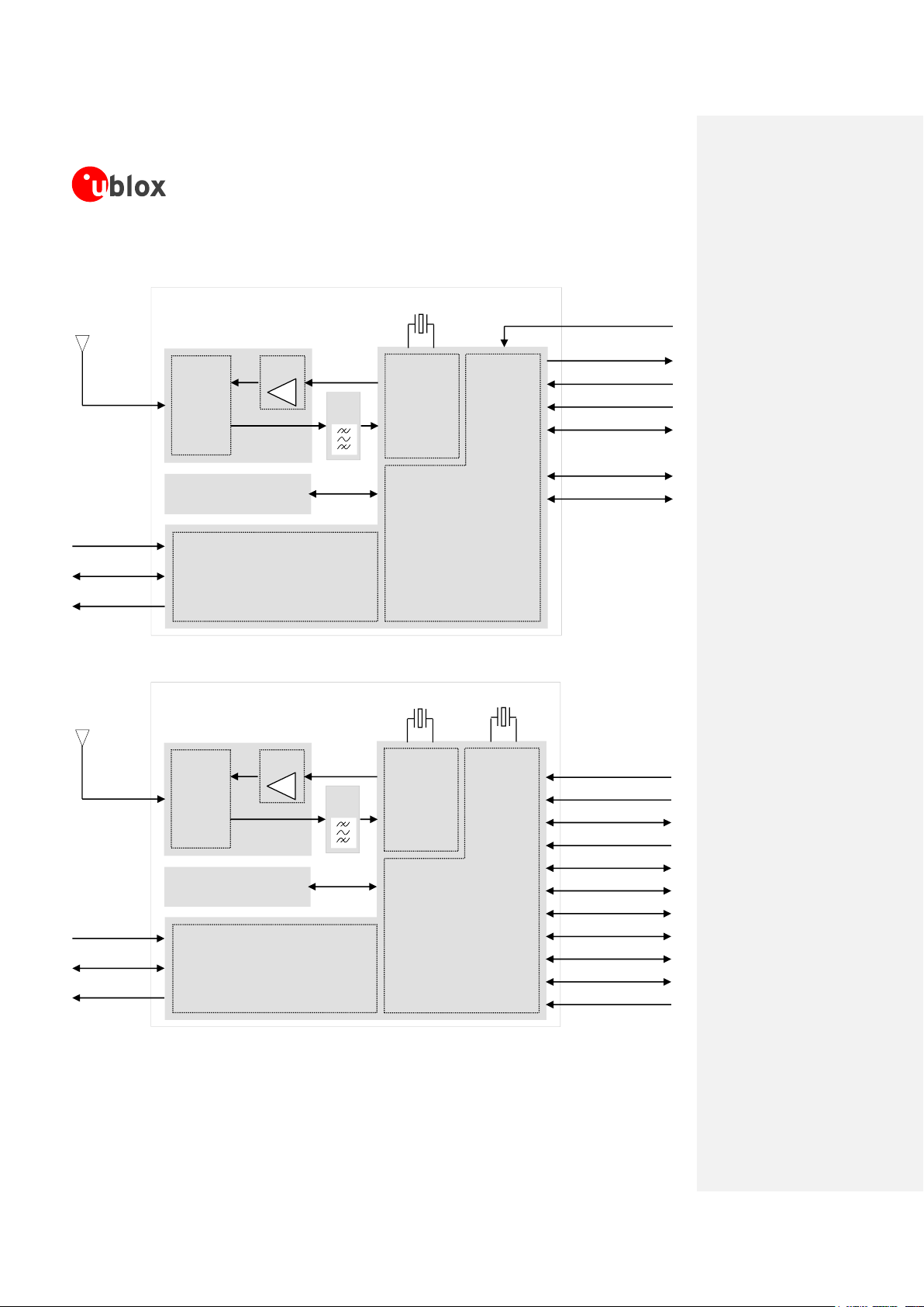
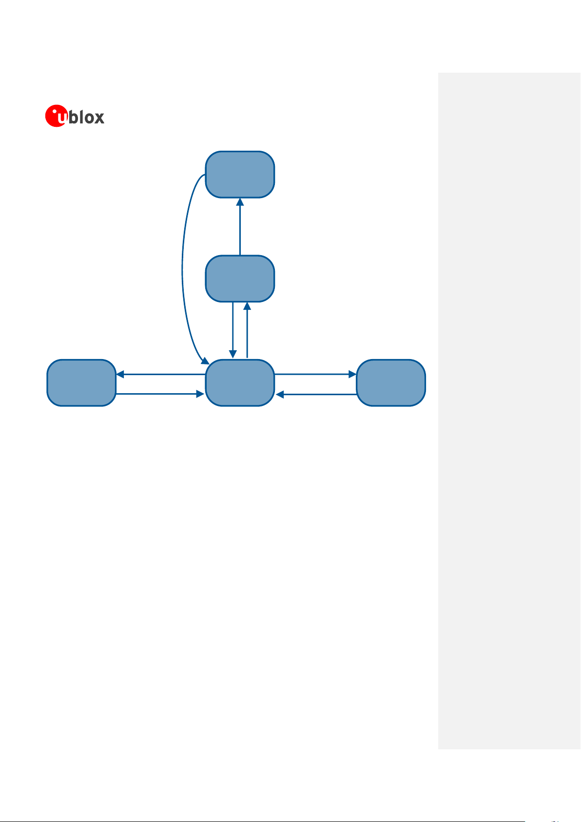
1.2 Architecture
Memory
V_BCKP (RTC)
V_INT (I/O)
32 kHz
26 MHz
RF
Transceiver
Power
Management
Baseband
ANT
SAW
Filter
Sw itch
PA
VCC (Supply)
32 kHz
Auxiliary UART
SIM Card
UART
Power-On
Reset
Memory
V_BCKP (RTC)
V_INT (I/O)
26 MHz
32.768 kHz
RF
Transceiver
Power
Management
Baseband
ANT
SAW
Filter
Switch
PA
VCC (Supply)
Auxiliary UART
DDC (for GNSS)
SIM Card Detection
SIM Card
UART
Power-On
Reset
Digital Audio
Analog Audio
GPIO
Antenna Detection
SARA-G3 series - System Integration Manual
Figure 1: SARA-G300 and SARA-G310 modules block diagram
Figure 2: SARA-G350 modules block diagram
UBX-13000995 - R06 Objective Specification System description
Page 13 of 218
Page 14

SARA-G3 series - System Integration Manual
UBX-13000995 - R06 Objective Specification System description
Page 14 of 218
Page 15

SARA-G3 series - System Integration Manual
1.2.1 Internal blocks
SARA-G3 modules consist of the following internal sections: RF, Baseband and Power Management.
RF section
The RF section is composed of the following main elements:
RF transceiver performing modulation, up-conversion of the baseband I/Q signals, down-conversion and
demodulation of the RF received signals. The RF transceiver includes:
Constant gain direct conversion receiver with integrated LNAs
Highly linear RF quadrature GMSK demodulator
Digital Sigma-Delta transmitter GMSK modulator
Fractional-N Sigma-Delta RF synthesizer
3.8 GHz VCO
Digital controlled crystal oscillator
Transmit module, which amplifies the signals modulated by the RF transceiver and connects the single
antenna input/output pin (ANT) of the module to the suitable RX/TX path, via its integrated parts:
Power amplifier
Antenna switch
RX diplexer SAW (band pass) filters
26 MHz crystal, connected to the digital controlled crystal oscillator to perform the clock reference in
active-mode or connected-mode
Baseband and Power Management section
The Baseband and Power Management section is composed of the following main elements:
Baseband processor, a mixed signal ASIC which integrates:
Microprocessor for controller functions
DSP core for GSM/GPRS Layer 1 and audio processing
Dedicated peripheral blocks for parallel control of the digital interfaces
Audio analog front-end
Memory system in a multi-chip package integrating two devices:
NOR flash non-volatile memory
PSRAM volatile memory
Voltage regulators to derive all the system supply voltages from the module supply VCC
SARA-G350 modules have an internal 32.768 kHz crystal connected to the oscillator of the RTC (Real
Time Clock) block that gives the RTC clock reference needed to provide the RTC functions as well as to
reach the very low power idle-mode (with power saving configuration enabled by the AT+UPSV
command).
SARA-G300 and SARA-G310 modules do not have an internal 32.768 kHz crystal: a proper 32 kHz
signal must be provided at the EXT32K input pin of the modules to give the RTC clock reference and to
provide the RTC functions as well as to reach the very low power idle-mode (with power saving
configuration enabled by the AT+UPSV command). The 32K_OUT output pin of SARA-G300 and SARA-
UBX-13000995 - R06 Objective Specification System description
Page 15 of 218
Page 16

SARA-G3 series - System Integration Manual
G310 modules provides a 32 kHz reference signal suitable only to feed the EXT32K input pin, furnishes
the reference clock for the RTC, and allows low power idle-mode and RTC functions support with modules
switched on.
UBX-13000995 - R06 Objective Specification System description
Page 16 of 218
Page 17
SARA-G3 series - System Integration Manual
Function
Pin Name
Module
Pin No
I/O
Description
Remarks
Power
VCC
All
51, 52,
53
I
Module supply
input
VCC pins are internally connected each other.
VCC supply circuit affects the RF performance
and compliance of the device integrating the
module with applicable required certification
schemes.
See section 1.5.11.5.1 for functional description
and requirements for the VCC module supply.
See section 2.1.12.1.1 for external circuit designin.
GND
All
1, 3, 5,
14,
20-22,
30, 32,
43, 50,
54, 55,
57-61,
63-96
N/A
Ground
GND pins are internally connected each other.
External ground connection affects the RF and
thermal performance of the device.
See section 1.5.11.5.1 for functional description.
See section 2.1.12.1.1 for external circuit designin.
V_BCKP
All 2 I/O
Real Time Clock
supply
input/output
V_BCKP = 2.3 V (typical) generated by
internal regulator when valid VCC supply is
present.
See section 1.5.21.5.2 for functional description.
See section 2.1.22.1.2 for external circuit designin.
V_INT
All 4 O
Digital Interfaces
supply output
V_INT = 1.8 V (typical) generated by internal
regulator when the module is switched on.
See section 1.5.31.5.3 for functional description.
See section 2.1.32.1.3 for external circuit designin.
System
PWR_ON
All
15 I Power-on input
High input impedance: input voltage level has to
be properly fixed, e.g. adding external pull-up.
See section 1.6.11.6.1 for functional description.
See section 2.2.12.2.1 for external circuit designin.
RESET_N
All
18 I External reset
input
A series Schottky diode is integrated in the
module as protection, and then an internal 10
k pull-up resistor to V_INT is provided.
See section 1.6.31.6.3 for functional description.
See section 2.2.22.2.2 for external circuit
design-in.
EXT32K
SARA-G300
SARA-G310
31 I 32 kHz input
Input for RTC reference clock, needed to enter
the low power idle-mode and provide RTC
functions.
See section 1.6.41.6.4 for functional description.
See section 2.2.32.2.3 for external circuit
design-in.
1.3 Pin-out
Table 3Table 3 lists the pin-out of the SARA-G3 modules, with pins grouped by function.
UBX-13000995 - R06 Objective Specification System description
Page 17 of 218
Page 18
SARA-G3 series - System Integration Manual
Function
Pin Name
Module
Pin No
I/O
Description
Remarks
32K_OUT
SARA-G300
SARA-G310
24 O 32 kHz output
32 kHz output suitable only to feed the EXT32K
input giving the RTC reference clock, allowing
low power idle-mode and RTC functions support.
See section 1.6.51.6.5 for functional description.
See section 2.2.32.2.3 for external circuit
design-in.
Antenna
ANT
All
56
I/O
RF input/output
for antenna
50 nominal characteristic impedance.
Antenna circuit affects the RF performance and
compliance of the device integrating the module
with applicable required certification schemes.
See section 1.7 for functional description and
requirements for the antenna RF interface.
See section 2.32.3 for external circuit design-in.
ANT_DET
SARA-G350
62 I Input for antenna
detection
ADC input for antenna detection function.
See section 1.7.2 for functional description.
See section 2.3.2 for external circuit design-in.
SIM
VSIM
All
41 O SIM supply
output
VSIM = 1.80 V typ. or 2.85 V typ.
automatically generated according to the connected
SIM type.
See section 1.81.8 for functional description.
See section 2.42.4 for external circuit design-in.
SIM_IO
All
39
I/O
SIM data
Data input/output for 1.8 V / 3 V SIM
Internal 4.7 k pull-up to VSIM.
See section 1.81.8 for functional description.
See section 2.42.4 for external circuit design-in.
SIM_CLK
All
38 O SIM clock
3.25 MHz clock output for 1.8 V / 3 V SIM
See section 1.81.8 for functional description.
See section 2.42.4 for external circuit design-in.
SIM_RST
All
40 O SIM reset
Reset output for 1.8 V / 3 V SIM
See section 1.81.8 for functional description.
See section 2.42.4 for external circuit design-in.
SIM_DET
All
42 I SIM detection
1.8 V input for SIM presence detection function.
See section 1.8.2 for functional description.
See section 2.4 for external circuit design-in.
UBX-13000995 - R06 Objective Specification System description
Page 18 of 218
Page 19
SARA-G3 series - System Integration Manual
Function
Pin Name
Module
Pin No
I/O
Description
Remarks
UART
RXD
All
13 O UART data
output
1.8 V output, Circuit 104 (RXD) in ITU-T
V.24,
for AT command, data communication, FOAT.
See section 1.9.11.9.1 for functional description.
See section 2.5.12.5.1 for external circuit designin.
TXD
All
12 I UART data input
1.8 V input, Circuit 103 (TXD) in ITU-T V.24,
for AT command, data communication, FOAT.
Internal active pull-up to V_INT.
See section 1.9.11.9.1 for functional description.
See section 2.5.12.5.1 for external circuit designin.
CTS
All
11 O UART clear to
send output
1.8 V output, Circuit 106 (CTS) in ITU-T
V.24,
for AT command, Data communication, FOAT.
See section 1.9.11.9.1 for functional description.
See section 2.5.12.5.1 for external circuit designin.
RTS
All
10 I UART ready to
send input
1.8 V input, Circuit 105 (RTS) in ITU-T V.24,
for AT command, data communication, FOAT.
Internal active pull-up to V_INT.
See section 1.9.11.9.1 for functional description.
See section 2.5.12.5.1 for external circuit designin.
DSR
All 6 O
UART data set
ready output
1.8 V output, Circuit 107 (DSR) in ITU-T
V.24,
for AT command, data communication, FOAT.
See section 1.9.11.9.1 for functional description.
See section 2.5.12.5.1 for external circuit designin.
RI
All 7 O
UART ring
indicator output
1.8 V output, Circuit 125 (RI) in ITU-T V.24,
for AT command, data communication, FOAT.
See section 1.9.11.9.1 for functional description.
See section 2.5.12.5.1 for external circuit designin.
DTR
All 9 I
UART data
terminal ready
input
1.8 V input, Circuit 108/2 (DTR) in ITU-T
V.24,
for AT command, data communication, FOAT.
Internal active pull-up to V_INT.
See section 1.9.11.9.1 for functional description.
See section 2.5.12.5.1 for external circuit designin.
DCD
All 8 O
UART data
carrier detect
output
1.8 V input, Circuit 109 (DCD) in ITU-T V.24,
for AT command, data communication, FOAT.
See section 1.9.11.9.1 for functional description.
See section 2.5.12.5.1 for external circuit designin.
UBX-13000995 - R06 Objective Specification System description
Page 19 of 218
Page 20
SARA-G3 series - System Integration Manual
Function
Pin Name
Module
Pin No
I/O
Description
Remarks
Auxiliary
UART
RXD_AUX
All
28 O Auxiliary UART
data output
1.8 V output, Circuit 104 (RXD) in ITU-T
V.24,
for FW upgrade and trace log capture.
Access by external test-point is recommended.
See section 1.9.21.9.2 for functional description.
See section 2.5.22.5.2 for external circuit
design-in.
TXD_AUX
All
29 I Auxiliary UART
data input
1.8 V input, Circuit 103 (TXD) in ITU-T V.24,
for FW upgrade and trace log capture.
Access by external test-point is recommended.
Internal active pull-up to V_INT.
See section 1.9.21.9.2 for functional description.
See section 2.5.22.5.2 for external circuit
design-in.
DDC
SCL
SARA-G350
27 O I2C bus clock
line
1.8 V open drain, for the communication with
u-blox positioning modules and chips.
External pull-up required.
See section 1.9.31.9.3 for functional description.
See section 2.5.32.5.3 for external circuit
design-in.
SDA
SARA-G350
26
I/O
I2C bus data line
1.8 V open drain, for the communication with
u-blox positioning modules and chips.
External pull-up required.
See section 1.9.31.9.3 for functional description.
See section 2.5.32.5.3 for external circuit
design-in.
UBX-13000995 - R06 Objective Specification System description
Page 20 of 218
Page 21
SARA-G3 series - System Integration Manual
Function
Pin Name
Module
Pin No
I/O
Description
Remarks
Analog
Audio
MIC_BIAS
SARA-G350
46 O Microphone
supply output
Supply output (2.2 V typ) for external
microphone.
See section 1.10.11.10.1 for functional description.
See section 2.6.12.6.1 for external circuit designin.
MIC_GND
SARA-G350
47 I Microphone
analog reference
Local ground for the external microphone
(reference for the analog audio uplink path).
See section 1.10.11.10.1 for functional description.
See section 2.6.12.6.1 for external circuit designin.
MIC_N
SARA-G350
48 I Differential analog
audio input
(negative)
Differential analog audio signal input (negative)
shared for all the analog uplink path modes:
handset, headset, hands-free mode.
No internal DC blocking capacitor.
See section 1.10.11.10.1 for functional description.
See section 2.6.12.6.1 for external circuit designin.
MIC_P
SARA-G350
49 I Differential analog
audio input
(positive)
Differential analog audio signal input (positive)
shared for all the analog uplink path modes:
handset, headset, hands-free mode.
No internal DC blocking capacitor.
See section 1.10.11.10.1 for functional description.
See section 2.6.12.6.1 for external circuit designin.
SPK_P
SARA-G350
44 O Differential analog
audio output
(positive)
Differential analog audio signal output (positive)
shared for all the analog downlink path modes:
earpiece, headset and loudspeaker mode.
See section 1.10.11.10.1 for functional description.
See section 2.6.12.6.1 for external circuit designin.
SPK_N
SARA-G350
45 O Differential analog
audio output
(negative)
Differential analog audio signal output (negative)
shared for all the analog downlink path modes:
earpiece, headset and loudspeaker mode.
See section 1.10.11.10.1 for functional description.
See section 2.6.12.6.1 for external circuit designin.
UBX-13000995 - R06 Objective Specification System description
Page 21 of 218
Page 22
SARA-G3 series - System Integration Manual
Function
Pin Name
Module
Pin No
I/O
Description
Remarks
Digital
Audio
I2S_CLK
SARA-G350
36 O I2S clock
1.8 V clock output for PCM / normal I2S
modes.
See section 1.10.21.10.2 for functional description.
See section 2.6.22.6.2 for external circuit
design-in.
I2S_RXD
SARA-G350
37 I I2S receive data
1.8 V data input for PCM / normal I2S modes.
Internal active pull-down to GND.
See section 1.10.21.10.2 for functional description.
See section 2.6.22.6.2 for external circuit
design-in.
I2S_TXD
SARA-G350
35 O I2S transmit data
1.8 V data output for PCM / normal I2S modes.
See section 1.10.21.10.2 for functional description.
See section 2.6.22.6.2 for external circuit
design-in.
I2S_WA
SARA-G350
34 O I2S word
alignment
1.8 V word al. output for PCM / normal I2S
modes
See section 1.10.21.10.2 for functional description.
See section 2.6.22.6.2 for external circuit
design-in.
GPIO
GPIO1
SARA-G350
16
I/O
GPIO
1.8 V GPIO by default configured as pad
disabled.
See section 1.111.11 for functional description.
See section 2.72.7 for external circuit design-in.
GPIO2
SARA-G350
23
I/O
GPIO
1.8 V GPIO by default configured to provide the
custom GNSS supply enable function.
See section 1.111.11 for functional description.
See section 2.72.7 for external circuit design-in.
GPIO3
SARA-G350
24
I/O
GPIO
1.8 V GPIO by default configured to provide the
custom GNSS data ready function.
See section 1.111.11 for functional description.
See section 2.72.7 for external circuit design-in.
GPIO4
SARA-G350
25
I/O
GPIO
1.8 V GPIO by default configured to provide the
custom GNSS RTC sharing function.
See section 1.111.11 for functional description.
See section 2.72.7 for external circuit design-in.
Reserved
RSVD
All
33
N/A
RESERVED pin
This pin must be connected to ground.
See section 2.82.8
RSVD
All
17, 19
N/A
RESERVED pin
Leave unconnected.
See section 2.82.8
RSVD
SARA-G350
31
N/A
RESERVED pin
Internally not connected. Leave unconnected.
See section 2.82.8
RSVD
SARA-G300
SARA-G310
16, 23,
25-27,
34-37
N/A
RESERVED pin
Pad disabled. Leave unconnected.
See section 2.82.8
RSVD
SARA-G300
SARA-G310
44-49,
62
N/A
RESERVED pin
Leave unconnected.
See section 2.82.8
Table 3: SARA-G3 series modules pin definition, grouped by function
UBX-13000995 - R06 Objective Specification System description
Page 22 of 218
Page 23

SARA-G3 series - System Integration Manual
UBX-13000995 - R06 Objective Specification System description
Page 23 of 218
Page 24
SARA-G3 series - System Integration Manual
General Status
Operating Mode
Definition
Power-down
Not-Powered Mode
VCC supply not present or below operating range: module is switched off.
Power-Off Mode
VCC supply within operating range and module is switched off.
Normal Operation
Idle-Mode
Module processor core runs with 32 kHz reference, that is generated by:
The internal 32 kHz oscillator (SARA-G350)
The 32 kHz signal provided at the EXT32K pin (SARA-G300 and SARA-
G310)
Active-Mode
Module processor core runs with 26 MHz reference generated by the internal
oscillator.
Connected-Mode
Voice or data call enabled and processor core runs with 26 MHz reference.
Operating Mode
Description
Transition between operating modes
Not-Powered Mode
Module is switched off.
Application interfaces are not accessible.
Internal RTC timer operates on SARA-G350
modules only if a valid voltage is applied to
V_BCKP pin. Additionally, a proper external 32 kHz
signal must be fed to EXT32K pin on SARA-G300
/ SARA-G310 to let RTC timer running that
otherwise is not in operation.
When VCC supply is removed, the module enters
not-powered mode.
When in not-powered mode, the module cannot be
switched on by a low level on PWR_ON input or by
a preset RTC alarm.
When in not-powered mode, the module can be
switched on applying VCC supply (refer to 2.2.1) so
that the module switches from not-powered to activemode.
Power-Off Mode
Module is switched off: normal shutdown by an
appropriate power-off event (refer to 1.6.2).
Application interfaces are not accessible.
Internal RTC timer operates on SARA-G350
modules.
A proper external 32 kHz signal must be fed to the
EXT32K pin on SARA-G300 / SARA-G310 to let
RTC timer running that otherwise is not in
operation.
When the module is switched off by an appropriate
power-off event (refer to 1.6.2), the module enters
power-off mode from active-mode.
When in power-off mode, the module can be
switched on by a low level on PWR_ON input or by
a preset RTC alarm (refer to 2.2.1): module
switches from power-off to active-mode.
When VCC supply is removed, the module switches
from power-off mode to not-powered mode.
1.4 Operating modes
SARA-G3 modules have several operating modes. The operating modes defined in Table 4Table 4 and
described in detail in Table 5Table 5 provide general guidelines for operation.
Table 4: Module operating modes definition
UBX-13000995 - R06 Objective Specification System description
Page 24 of 218
Page 25
SARA-G3 series - System Integration Manual
Operating Mode
Description
Transition between operating modes
Idle-Mode
The module is not ready to communicate with an
external device by means of the application
interfaces since configured to reduce power
consumption.
The module automatically enters idle-mode whenever
possible if power saving is enabled by the
AT+UPSV command (refer to
u-blox AT Commands
Manual
[2]), reducing power consumption (refer to
1.5.1.3).
The CTS output line indicates when the UART
interface is disabled/enabled due to the module
idle/active-mode according to power saving and
hardware flow control settings (refer to 1.9.1.3,
1.9.1.4).
Power saving configuration is not enabled by default:
it can be enabled by the AT+UPSV command (see
u-blox AT Commands Manual
[2]).
A proper 32 kHz signal must be fed to the EXT32K
pin of SARA-G300 and SARA-G310 modules to let
idle-mode that otherwise cannot be reached (this is
not needed for the other SARA-G3 series
modules).
The module automatically switches from active-mode
to idle-mode whenever possible if power saving is
enabled (refer to sections 1.5.1.3, 1.9.1.4 and to the
u-blox AT Commands Manual
[2], AT+UPSV).
The module wakes up from idle-mode to active-mode
in the following events:
Automatic periodic monitoring of the paging
channel for the paging block reception according
to network conditions (refer to 1.5.1.3, 1.9.1.4)
Automatic periodic enable of the UART interface
to receive and send data, if the power saving
AT command is set to 1 (refer to 1.9.1.4)
RTC alarm occurs (refer to
u-blox AT
Commands Manual
[2], AT+CALA command)
Data received on UART interface (refer to
1.9.1.4)
RTS input line set to the ON state by the DTE
if hardware flow control has been disabled by
AT&K3 and the power saving AT command is
set to 2 (refer to 1.9.1.4)
GNSS data ready: when the GPIO3 pin is
informed by the connected u-blox GNSS receiver
that it is ready to send data via the DDC
(I2C) interface (refer to 1.11, 1.9.3)
Active-Mode
The module is ready to communicate with an
external device by means of the application
interfaces unless power saving configuration is
enabled by the AT+UPSV command (refer to
sections 1.5.1.3, 1.9.1.4 and to the
u-blox AT
Commands Manual
[2]).
When the module is switched on by an appropriate
power-on event (refer to 2.2.1), the module enters
active-mode from not-powered or power-off mode.
If power saving configuration is enabled by the
AT+UPSV command, the module automatically
switches from active to idle-mode whenever possible
and the module wakes up from idle to active-mode
in the events listed above (refer to idle to active
transition description).
When a voice call or a data call is initiated, the
module switches from active-mode to connectedmode.
Connected-Mode
A voice call or a data call is in progress.
The module is ready to communicate with an
external device by means of the application
interfaces unless power saving configuration is
enabled by the AT+UPSV command (see sections
1.5.1.3, 1.9.1.4 and the
u-blox AT Commands
Manual
[2][2]).
When a voice call or a data call is initiated, the
module enters connected-mode from active-mode.
When a voice call or a data call is terminated, the
module returns to the active-mode.
Table 5: Module operating modes description
Figure 3Figure 3 describes the transition between the different operating modes.
UBX-13000995 - R06 Objective Specification System description
Page 25 of 218
Page 26
SARA-G3 series - System Integration Manual
Switch ON:
• Apply VCC
If power saving is enabled
and there is no activity for
a defined time interval
Any wake up event described
in the module operating
modes summary table above
Incoming/outgoing call or
other dedicated device
network communication
Call terminated,
communication dropped
Remove VCC
Switch ON:
• PWR_ON
• RTC Alarm
Not
powered
Power off
ActiveConnected Idle
Switch OFF:
• AT+CPWROFF
Figure 3: Operating modes transition
UBX-13000995 - R06 Objective Specification System description
Page 26 of 218
Page 27
SARA-G3 series - System Integration Manual
Item
Requirement
Remark
VCC nominal voltage
Within VCC normal operating range:
3.35 V min. / 4.50 V max.
The module cannot be switched on if VCC voltage
value is below the normal operating range minimum
limit.
Ensure that the input voltage at VCC pins is above
the minimum limit of the normal operating range for at
least more than 3 s after the module switch-on.
VCC voltage during
normal operation
Within VCC extended operating range:
3.00 V min. / 4.50 V max.
The module may switch off when VCC voltage drops
below the extended operating range minimum limit.
Operation above extended operating range maximum
limit is not recommended and exposure beyond it may
affect device reliability.
VCC average current
Considerably withstand maximum average current
consumption value in connected-mode conditions
specified in
SARA-G3 series Data Sheet
[1][1].
The maximum average current consumption can be
greater than the specified value according to the actual
antenna mismatching, temperature and VCC voltage.
Section 1.5.1.21.5.1.2 describes connected-mode
current.
1.5 Supply interfaces
1.5.1 Module supply input (VCC)
SARA-G3 modules must be supplied via the three VCC pins that represent the module power supply
input.
The VCC pins are internally connected to the RF power amplifier and to the integrated Power Management
Unit: all supply voltages needed by the module are generated from the VCC supply by integrated voltage
regulators, including V_BCKP Real Time Clock supply, V_INT digital interfaces supply and VSIM SIM card
supply.
During operation, the current drawn by the SARA-G3 series modules through the VCC pins can vary by
several orders of magnitude. This ranges from the high peak of current consumption during GSM
transmitting bursts at maximum power level in connected-mode (as described in section 1.5.1.2), to the
low current consumption during low power idle-mode with power saving enabled (as described in section
1.5.1.3).
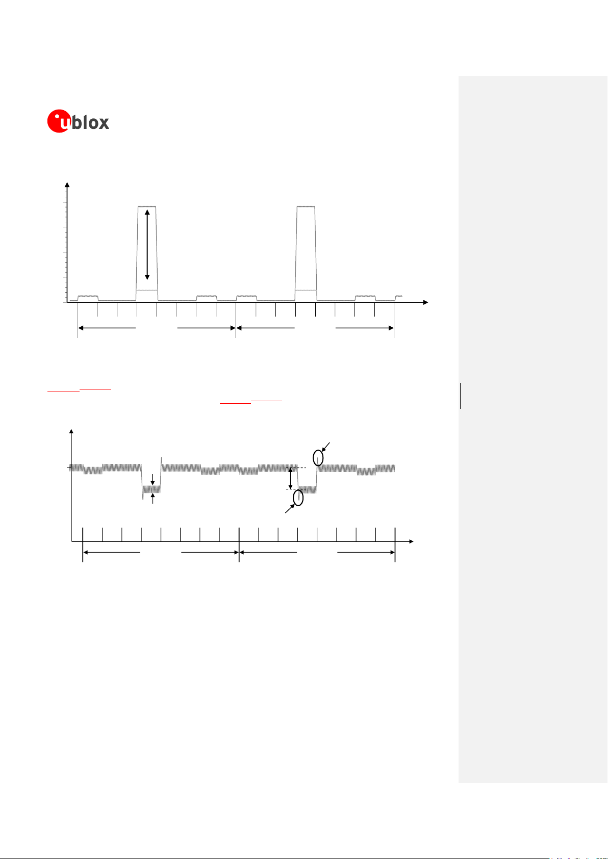
1.5.1.1 VCC supply requirements
Table 6Table 6 summarizes the requirements for the VCC module supply. Refer to section 2.1.1 for all
the suggestions to properly design a VCC supply circuit compliant to the requirements listed in Table
6Table 6.
The VCC supply circuit affects the RF compliance of the device integrating SARA-G3 series module with
applicable required certification schemes as well as antenna circuit design. Compliance is guaranteed if
the VCC requirements summarized in the Table 6Table 6 are fulfilled.
UBX-13000995 - R06 Objective Specification System description
Page 27 of 218
Formatted: Font: 8 pt
Formatted: Font: 8 pt, French
(France)
Page 28
Item
Requirement
Remark
VCC peak current
Withstand the maximum peak current consumption
specified in the
SARA-G3 series Data
Sheet
[1][1].
The specified maximum peak of current consumption
occurs during GSM single transmit slot in 850/900
MHz connected-mode, in case of mismatched antenna.
Section 1.5.1.21.5.1.2 describes connected-mode
current.
VCC voltage drop
during Tx slots
Lower than 400 mV
VCC voltage drop values greater than recommended
during 2G TDMA transmission slots directly affect the
RF compliance with applicable certification schemes.
Figure 5Figure 5 describes VCC voltage drop during
Tx slots.
VCC voltage ripple
during Tx slots
Lower than 30 mVpp if f
ripple
≤ 200 kHz
Lower than 10 mVpp if 200 kHz < f
ripple
≤ 400
kHz
Lower than 2 mVpp if f
ripple
> 400 kHz
VCC voltage ripple values higher than recommended
during 2G transmission directly affect the RF
compliance with applicable certification schemes.
Figure 5Figure 5 describes VCC voltage ripple during
Tx slots.
VCC under/over-shoot
at start/end of Tx
slots
Absent or at least minimized
VCC under/over-shoot higher than recommended at
the start/end of 2G TDMA transmission slots directly
affect the RF compliance with applicable certification
schemes.
Figure 5Figure 5 describes VCC voltage under/over-
shoot at the start/end of Tx slots
Table 6: Summary of VCC supply requirements
SARA-G3 series - System Integration Manual
Formatted: Font: 8 pt
Formatted: Font: 8 pt, French
(France)
Formatted: Font: 8 pt
Formatted: Font: 8 pt
Formatted: Font: 8 pt
For the additional specific requirement for SARA-G350 ATEX modules integration in potentially
explosive atmospheres applications, refer to section 2.13.
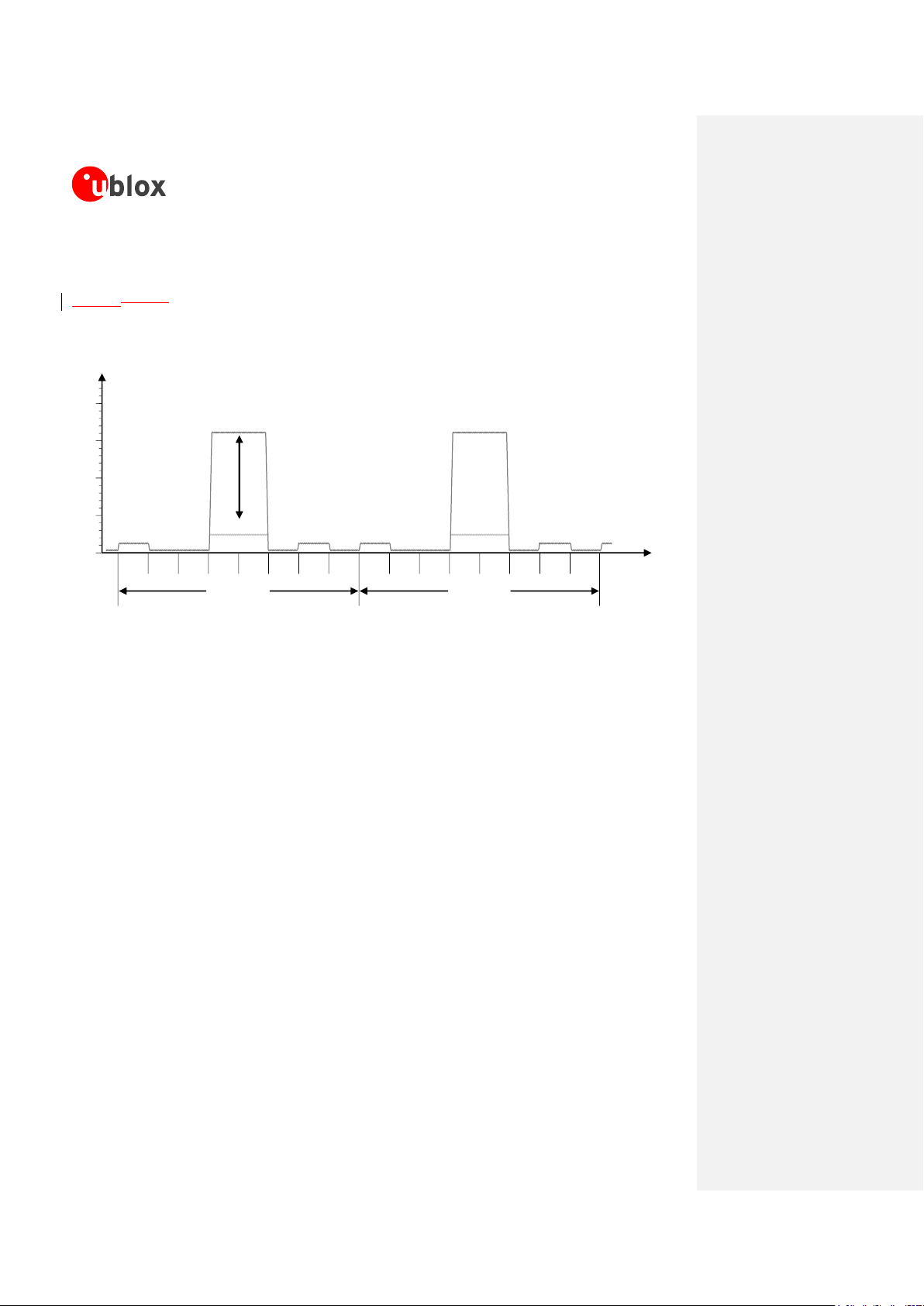
1.5.1.2 VCC current consumption in connected-mode
When a GSM call is established, the VCC consumption is determined by the current consumption profile
typical of the GSM transmitting and receiving bursts.
The current consumption peak during a transmission slot is strictly dependent on the transmitted power,
which is regulated by the network. If the module is transmitting in GSM talk mode in the 850 or 900
MHz bands, at the maximum RF power control level (approximately 2 W or 33 dBm in the allocated
transmit slot/burst) the current consumption can reach up to 1900 mA (with a highly unmatched
antenna) for 576.9 µs (width of the transmit slot/burst) with a periodicity of 4.615 ms (width of 1
frame = 8 slots/burst), so with a 1/8 duty cycle according to GSM TDMA (Time Division Multiple
Access). If the module is in GSM connected-mode in the 1800 or 1900 MHz bands, the current
consumption figures are lower than the one in the 850 or 900 MHz bands, due to 3GPP transmitter
output power specifications (refer to
During a GSM call, current consumption is in the order of 60-120 mA in receiving or in monitor bursts
and is about 10-40 mA in the inactive unused bursts (low current period). The more relevant factor for
determining the average current consumption, is the transmitted power in the transmit slot.
Figure 4Figure 4 shows an example of the module current consumption profile versus time in GSM talk
mode.
SARA-G3 series Data Sheet
[1]).
UBX-13000995 - R06 Objective Specification System description
Page 28 of 218
Page 29
SARA-G3 series - System Integration Manual
Time [ms]
RX
slot
unused
slot
unused
slot
TX
slot
unused
slot
unused
slot
MON
slot
unused
slot
RX
slot
unused
slot
unused
slot
TX
slot
unused
slot
unused
slot
MON
slot
unused
slot
GSM frame
4.615 ms
(1 frame = 8 slots)
Current [A]
200 mA
60-120 mA
1900 mA
Peak current
depends on
TX power
GSM frame
4.615 ms
(1 frame = 8 slots)
1.5
1.0
0.5
0.0
2.0
60-120 mA
10-40 mA
Time
undershoot
overshoot
ripple
drop
Voltage
3.8 V
(typ)
RX
slot
unused
slot
unused
slot
TX
slot
unused
slot
unused
slot
MON
slot
unused
slot
RX
slot
unused
slot
unused
slot
TX
slot
unused
slot
unused
slot
MON
slot
unused
slot
GSM frame
4.615 ms
(1 frame = 8 slots)
GSM frame
4.615 ms
(1 frame = 8 slots)
Figure 4: VCC current consumption profile versus time during a GSM call (1 TX slot, 1 RX slot)
Figure 5Figure 5 illustrates VCC voltage profile versus time during a GSM call, according to the relative
VCC current consumption profile described in Figure 4Figure 4.
Figure 5: Description of the VCC voltage profile versus time during a GSM call
When a GPRS connection is established, more than one slot can be used to transmit and/or more than
one slot can be used to receive. The transmitted power depends on network conditions, which set the
peak current consumption, but following the GPRS specifications the maximum transmitted RF power is
reduced if more than one slot is used to transmit, so the maximum peak of current is not as high as
can be in case of a GSM call.
If the module transmits in GPRS multi-slot class 10, in the 850 or 900 MHz bands, at the maximum
power control level, the consumption can reach up to 1600 mA (with highly unmatched antenna). This
happens for 1.154 ms (width of the 2 Tx slots/bursts) with a periodicity of 4.615 ms (width of 1 frame
UBX-13000995 - R06 Objective Specification System description
Page 29 of 218
Page 30
SARA-G3 series - System Integration Manual
Time [ms]
RX
slot
unused
slot
unused
slot
TX
slot
TX
slot
unused
slot
MON
slot
unused
slot
RX
slot
unused
slot
unused
slot
TX
slot
TX
slot
unused
slot
MON
slot
unused
slot
GSM frame
4.615 ms
(1 frame = 8 slots)
Current [A]
60-120mA
GSM frame
4.615 ms
(1 frame = 8 slots)
1.5
1.0
0.5
0.0
2.0
60-120mA
10-40mA
200mA
Peak current
depends on
TX power
1600 mA
= 8 slots/bursts), so with a 1/4 duty cycle, according to GSM TDMA. If the module is in GPRS
connected-mode in 1800 or 1900 MHz bands, consumption figures are lower than in the 850 or 900
MHz band, due to 3GPP Tx power specifications.
Figure 6Figure 6 reports the current consumption profiles in GPRS connected-mode, in the 850 or 900
MHz bands, with 2 slots used to transmit and 1 slot used to receive.
Figure 6: VCC current consumption profile versus time during a GPRS connection (2 TX slots, 1 RX slot)
UBX-13000995 - R06 Objective Specification System description
Page 30 of 218
Page 31

SARA-G3 series - System Integration Manual
1.5.1.3 VCC current consumption in cyclic idle/active-mode (power saving enabled)
The power saving configuration is by default disabled, but it can be enabled using the appropriate AT
command (refer to
u-blox AT Commands Manual
[2], AT+UPSV command). When power saving is
enabled, the module automatically enters idle-mode whenever possible, reducing current consumption.
During idle-mode, the module processor runs with 32 kHz reference clock frequency. For SARA-G350
modules, the internal oscillator automatically generates the 32 kHz clock. For SARA-G300 and SARAG310 modules, a valid 32 kHz signal must be properly provided to the EXT32K input pin of the module
to let idle-mode, that otherwise cannot be reached (this is not needed for the other SARA-G3 series
modules).
When power saving is enabled, the module is registered or attached to a network and a voice or data
call is not enabled, the module automatically enters idle-mode whenever possible, but it must periodically
monitor the paging channel of the current base station (paging block reception), in accordance to GSM
system requirements. When the module monitors the paging channel, it wakes up to active-mode, to
enable the reception of paging block. In between, the module switches to idle-mode. This is known as
GSM discontinuous reception (DRX).
The module processor core is activated during the paging block reception, and automatically switches its
reference clock frequency from 32 kHz to the 26 MHz used in active-mode.
The time period between two paging block receptions is defined by the network. This is the paging period
parameter, fixed by the base station through broadcast channel sent to all users on the same serving cell.
The time interval between two paging block receptions can be from 470.76 ms (DRX = 2, i.e. width of
2 GSM multiframes = 2 x 51 GSM frames = 2 x 51 x 4.615 ms) up to 2118.42 ms (DRX = 9, i.e.
width of 9 GSM multiframes = 9 x 51 frames = 9 x 51 x 4.615 ms).
Figure 7Figure 7 roughly describes the current consumption profile of SARA-G350 modules, or specifically
of SARA-G300 / SARA-G310 modules when their EXT32K input pin is fed by an external 32 kHz signal
with characteristics compliant to the one specified in
SARA-G3 series Data Sheet
[1], when power saving
is enabled. The module is registered with the network, automatically enters the very low power idle-mode,
and periodically wakes up to active-mode to monitor the paging channel for paging block reception.
UBX-13000995 - R06 Objective Specification System description
Page 31 of 218
Page 32

SARA-G3 series - System Integration Manual
20-30 ms
IDLE MODE ACTIVE MODE IDLE MODE
300-600 µA
Active Mode
Enabled
Idle Mode
Enabled
300-600 µA
60-120 mA
0.44-2.09 s
IDLE MODE
20-30 ms
ACTIVE MODE
Time [s]
Current [mA]
100
50
0
Time [ms]
Current [mA]
100
50
0
4-5 mA
60-120 mA
RX
Enabled
20-40 mA
DSP
Enabled
Figure 7: VCC current consumption profile versus time of the SARA-G350 modules or the SARA-G300 / SARA-G310 modules (with the
EXT32K input fed by a proper external 32 kHz signal), when registered with the network, with power saving enabled: the very low power
idle-mode is reached and periodical wake up to active-mode are performed to monitor the paging channel
Figure 8Figure 8 roughly describes the current consumption profile of SARA-G300 / SARA-G310 modules
when the EXT32K input pin is fed by the 32K_OUT output pin provided by these modules, when power
saving is enabled. The module is registered with the network, automatically enters the low power idlemode and periodically wakes up to active-mode to monitor the paging channel for paging block reception.
UBX-13000995 - R06 Objective Specification System description
Page 32 of 218
Page 33

SARA-G3 series - System Integration Manual
20-30 ms
IDLE MODE ACTIVE MODE IDLE MODE
3-4 mA
Active Mode
Enabled
Idle Mode
Enabled
3-4 mA
60-120 mA
0.44-2.09 s
IDLE MODE
20-30 ms
ACTIVE MODE
Time [s]
Current [mA]
100
50
0
Time [ms]
Current [mA]
100
50
0
4-5 mA
60-120 mA
RX
Enabled
20-40 mA
DSP
Enabled
Figure 8: VCC current consumption profile versus time of the SARA-G300 / SARA-G310 modules (with the EXT32K input pin fed by the
32K_OUT output pin provided by these modules), when registered with the network, with power saving enabled:
the low power idle-mode is reached and periodical wake up to active-mode are performed to monitor the paging channel
UBX-13000995 - R06 Objective Specification System description
Page 33 of 218
Page 34

SARA-G3 series - System Integration Manual
ACTIVE MODE
60-120 mA
0.47-2.12 s
Paging period
Time [s]
Current [mA]
100
50
0
Time [ms]
Current [mA]
100
50
0
3-5 mA
60-120 mA
RX
Enabled
20-40 mA
DSP
Enabled
3-5 mA
3-5 mA
1.5.1.4 VCC current consumption in fixed active-mode (power saving disabled)
Power saving configuration is by default disabled, or it can be disabled using the appropriate AT command
(refer to
u-blox AT Commands Manual
[2], AT+UPSV command). When power saving is disabled, the
module does not automatically enter idle-mode whenever possible: the module remains in active-mode.
The module processor core is activated during active-mode, and the 26 MHz reference clock frequency is
used.
Figure 9Figure 9 roughly describes the current consumption profile of SARA-G300 / SARA-G310 modules
when the EXT32K input pin is fed by external 32 kHz signal with characteristics compliant to the one
specified in
SARA-G3 series Data Sheet
[1], or by the 32K_OUT output pin provided by these modules,
when power saving is disabled. The module is registered with the network, active-mode is maintained, and
the receiver and the DSP are periodically activated to monitor the paging channel for paging block
reception.
Figure 9: VCC current consumption profile versus time of the SARA-G300 / SARA-G310 modules (with the EXT32K input pin fed by proper
external 32 kHz signal or by 32K_OUT output pin), when registered with the network, with power saving disabled:
the active-mode is always held, and the receiver and the DSP are periodically activated to monitor the paging channel
UBX-13000995 - R06 Objective Specification System description
Page 34 of 218
Page 35

SARA-G3 series - System Integration Manual
ACTIVE MODE
15-18 mA
60-120 mA
0.47-2.12 s
Paging period
Time [s]
Current [mA]
100
50
0
Time [ms]
Current [mA]
100
50
0
15-18 mA
60-120 mA
RX
Enabled
20-40 mA
DSP
Enabled
15-18 mA
Figure 10Figure 10 roughly describes the current consumption profile of SARA-G350 modules or the
current consumption profile of SARA-G300 / SARA-G310 modules when their EXT32K input is not fed
by a signal (left unconnected), when power saving is disabled: the module is registered with the network,
active-mode is maintained, and the receiver and the DSP are periodically activated to monitor the paging
channel for paging block reception.
Figure 10: VCC current consumption profile versus time of the SARA-G350 modules or the SARA-G300 / SARA-G310 modules (with the
EXT32K input pin not fed by any 32 kHz signal), when registered with the network, with power saving disabled:
the active-mode is always held, and the receiver and the DSP are periodically activated to monitor the paging channel
UBX-13000995 - R06 Objective Specification System description
Page 35 of 218
Page 36

SARA-G3 series - System Integration Manual
Baseband
Processor
51
VCC
52
VCC
53
VCC
2
V_BCKP
Linear
LDO
RTC
Power
Management
SARA-G350
32 kHz
Baseband
Processor
51
VCC
52
VCC
53
VCC
2
V_BCKP
Linear
LDO
RTC
Power
Management
SARA-G300 / SARA-G310
32 kHz
31
EXT32K
V_BCKP voltage value
RTC value reliability
Notes
1.00 V < V_BCKP < 2.40 V
RTC oscillator does not stop operation
RTC value read after a restart of the system is reliable
V_BCKP within operating range
0.05 V < V_BCKP < 1.00 V
RTC oscillator does not necessarily stop operation
RTC value read after a restart of the system is not
reliable
V_BCKP below operating range
0.00 V < V_BCKP < 0.05 V
RTC oscillator stops operation
RTC value read after a restart of the system is reliable
V_BCKP below operating range
1.5.2 RTC supply input/output (V_BCKP)
The V_BCKP pin of SARA-G3 modules connects the supply for the Real Time Clock (RTC) and PowerOn internal logic. This supply domain is internally generated by a linear LDO regulator integrated in the
Power Management Unit, as described in Figure 11Figure 11. The output of this linear regulator is always
enabled when the main voltage supply provided to the module through the VCC pins is within the valid
operating range, with the module switched off or switched on.
Figure 11: SARA-G3 series RTC supply input/output (V_BCKP) and 32 kHz RTC timing reference clock simplified block diagram
The RTC provides the module time reference (date and time) that is used to set the wake-up interval
during the idle-mode periods between network paging, and is able to make available the programmable
alarm functions.
The RTC functions are available also in power-down mode when the V_BCKP voltage is within its valid
range (specified in the “Input characteristics of Supply/Power pins” table in
Sheet
[1]) and, for SARA-G300 / SARA-G310 modules only, when their EXT32K input pin is fed by
an external 32.768 kHz signal with proper characteristics (specified in the “EXT32K pin characteristics”
table in
SARA-G3 series Data Sheet
[1]).
The RTC can be supplied from an external back-up battery through the V_BCKP, when the main voltage
supply is not provided to the module through VCC. This lets the time reference (date and time) run until
the V_BCKP voltage is within its valid range, even when the main supply is not provided to the module.
The RTC oscillator does not necessarily stop operation (i.e. the RTC counting does not necessarily stop)
when V_BCKP voltage value drops below the specified operating range minimum limit (1.00 V): the RTC
value read after a system restart could be not reliable, as explained in Table 7Table 7.
SARA-G3 series Data
UBX-13000995 - R06 Objective Specification System description
Page 36 of 218
Page 37

SARA-G3 series - System Integration Manual
Baseband
Processor
51
VCC
52
VCC
53
VCC
4
V_INT
Switching
Step-Down
Digital I/O
Interfaces
Power
Management
SARA-G3 series
Table 7: RTC value reliability as function of V_BCKP voltage value
Consider that the module cannot switch on if a valid voltage is not present on VCC even when the RTC
is supplied through V_BCKP (meaning that VCC is mandatory to switch on the module).
The RTC has very low power consumption, but is highly temperature dependent. For example at 25 °C,
with the V_BCKP voltage equal to the typical output value, the power consumption is approximately 2 µA
(refer to the “Input characteristics of Supply/Power pins” table in the
SARA-G3 series Data Sheet
[1] for
the detailed specification), whereas at 70 °C and an equal voltage the power consumption increases to
5-10 µA.
If V_BCKP is left unconnected and the module main voltage supply is removed from VCC, the RTC is
supplied from the bypass capacitor mounted inside the module. However, this capacitor is not able to
provide a long buffering time: within few milliseconds the voltage on V_BCKP will go below the valid
range (1 V min). This has no impact on wireless connectivity, as all the module functionalities do not
rely on date and time setting.
1.5.3 Interfaces supply output (V_INT)
The same 1.8 V voltage domain used internally to supply the digital interfaces of SARA-G3 modules is
also available on the V_INT supply output pin, as described in Figure 12Figure 12.
Figure 12: SARA-G3 series interfaces supply output (V_INT) simplified block diagram
The internal regulator that generates the V_INT supply is a switching step-down converter that is directly
supplied from VCC. The voltage regulator output is set to 1.8 V (typical) when the module is switched
on and it is disabled when the module is switched off.
The switching regulator operates in Pulse Width Modulation (PWM) for greater efficiency at high output
loads when the module is in active-mode or in connected-mode. When the module is in low power idlemode between paging periods and with power saving configuration enabled by the appropriate AT
command, it automatically switches to Pulse Frequency Modulation (PFM) for greater efficiency at low
output loads. Refer to the
u-blox AT Commands Manual
[2], +UPSV command.
UBX-13000995 - R06 Objective Specification System description
Page 37 of 218
Page 38

SARA-G3 series - System Integration Manual
1.6 System function interfaces
1.6.1 Module power-on
The power-on sequence of SARA-G3 series modules is initiated in one of these ways:
Rising edge on the VCC pin to a valid voltage as module supply (i.e. applying module supply)
Low level on the PWR_ON pin (normally high with external pull-up) for an appropriate time period
RTC alarm (i.e. pre-programmed scheduled time by AT+CALA command)
1.6.1.1 Rising edge on VCC
When a SARA-G3 module is in the not-powered mode, it can be switched on by applying the VCC
supply.
The module is switched on when the voltage rises up to the VCC normal operating range minimum limit
(3.35 V) starting from a voltage value lower than 2.25 V, and with a proper voltage slope: the voltage
at the VCC pins must ramp from 2.5 V to 3.2 V within 4 ms to switch on the module. When the VCC
voltage is stabilized at its nominal value within the normal operating range, the module can be switched
on by a low level on PWR_ON pin (see section 1.6.1.2) or by RTC alarm (see section 1.6.1.3).
If the PWR_ON input pin is held low during the VCC apply phase, the SARA-G3 module switches on
when voltage rises up to the VCC normal operating range minimum limit (3.35 V).
1.6.1.2 Low level on PWR_ON
When a SARA-G3 module is in the power-off mode (i.e. switched off with valid VCC supply
maintained), the module can be switched on by forcing a low level on the PWR_ON input pin at least
for 5 ms.
The electrical characteristics of the PWR_ON input pin are different from the other digital I/O interfaces.
The input voltage thresholds are slightly different since the PWR_ON input pin is tolerant of voltages up to
the module supply level. The detailed electrical characteristics are described in
Sheet
[1].
There is no internal pull-up resistor on the PWR_ON pin: the pin has high input impedance and is
weakly pulled to the high level by the internal circuit. Therefore the external circuit must be able to hold
the high logic level stable, e.g. providing an external pull-up resistor (for further design-in guidelines refer
to section 2.2.1).
1.6.1.3 RTC alarm
When a SARA-G3 module is in the power-off mode (i.e. switched off with valid VCC supply
maintained) and the RTC timing (32 kHz reference clock) is available, the module can be switched on
by an RTC alarm previously programmed by AT command at a scheduled time (refer to the
Commands Manual
boot sequence by instructing the Power Management Unit to turn on power. Also included in this setup is
an interrupt signal from the RTC block to indicate to the baseband processor that an RTC event has
occurred.
The RTC timing is automatically generated by the 32.768 kHz reference clock provided by the internal
oscillator on SARA-G350 modules. A valid external 32.768 kHz signal must be provided at the EXT32K
[2], AT+CALA command). The internal RTC block system will then initiate the module
SARA-G3 series Data
u-blox AT
UBX-13000995 - R06 Objective Specification System description
Page 38 of 218
Page 39

SARA-G3 series - System Integration Manual
VCC
V_BCKP
PWR_ON
V_INT
Internal Reset
System State
BB Pads State
Internal Reset → Operational Operational
Tristate / Floating
Internal Reset
OFF
ON
Start-up
event
PWR_ON
can be set high
Start of interface
configuration
All interfaces
are configured
input pin of the SARA-G300 / SARA-G310 modules to enable RTC timing, otherwise the switch-on of
SARA-G300 / SARA-G310 modules by means of a pre-programmed RTC alarm is not possible (refer to
section 1.6.4).
1.6.1.4 Additional considerations
The module is switched on when the VCC voltage rises to the normal operating range (i.e. applying
module supply): the first time that the module is used, it is switched on in this way. SARA-G3 modules
can be switched off by means of the AT+CPWROFF command, entering power-off mode. In this state,
the digital input-output pads of the baseband chipset (i.e. all the digital pins of the module) are locked
in tri-state (i.e. floating). The power down tri-state function isolates the module pins from the
environment, when no proper operation of the outputs can be guaranteed.
The module can be switched on from power-off mode by forcing a proper start-up event (e.g. PWR_ON
low). After the detection of a start-up event, all the module digital pins are held in tri-state until all the
internal LDO voltage regulators are turned on in a defined power-on sequence. Then, as described in
Figure 13Figure 13, the baseband core is still held in reset state for a time interval: the internal reset
signal (which is not available on a module pin) is still low and all the digital pins of the module are
held in reset state. The reset state of all the digital pins is reported in the pin description table of
SARA-G3 Series Data Sheet
[1]. When the internal signal is released, the configuration of the module
interfaces starts: during this phase any digital pin is set in a proper sequence from the reset state to the
default operational configuration. Finally, the module is fully ready to operate when all interfaces are
configured.
Figure 13: SARA-G3 series power-on sequence description
The Internal Reset signal is not available on a module pin, but the application can monitor the
UBX-13000995 - R06 Objective Specification System description
Page 39 of 218
V_INT pin to sense the start of the SARA-G3 series power-on sequence.
Page 40

SARA-G3 series - System Integration Manual
VCC
V_BCKP
PWR_ON
V_INT
Internal Reset
System State
BB Pads State Operational
OFF
Tristate / Floating
ON
Operational → Tristate / Floating
AT+CPWROFF
sent to the module
OK
replied by the module
1.6.2 Module power-off
The correct way to switch off SARA-G3 modules is by means of +CPWROFF AT command (more details
in
u-blox AT Commands Manual
module’s non-volatile memory and a proper network detach is performed.
An under-voltage shutdown occurs on SARA-G3 modules when the VCC supply is removed, but in this
case the current parameter settings are not saved in the module’s non-volatile memory and a proper
network detach cannot be performed.
An over-temperature or an under-temperature shutdown occurs when the temperature measured within the
wireless module reaches the dangerous area, if the optional Smart Temperature Supervisor feature is
activated and configured by the dedicated AT+USTS command. Refer to section 1.13.8 and to the
AT Commands Manual
[2] for more details.
Figure 14Figure 14 describes the power-off sequence by means of +CPWROFF AT command. When the
+CPWROFF AT command is sent, the module starts the switch-off routine replying OK on the AT
interface. At the end of the switch-off routine, all digital pins are locked in tri-state by the module and
all the internal LDO voltage regulators except the RTC supply (V_BCKP) are turned off in a defined
power-off sequence. The module remains in power-off mode as long as a switch on event does not
occur (i.e. applying a low level on the PWR_ON pin, or by a pre-programmed RTC alarm), and enters
not-powered mode if the supply is removed from the VCC pin.
Current parameter settings are stored to the module’s non-volatile memory and a network detach is
performed before the OK reply from AT+CPWROFF command.
The duration of the switch-off routine phases can largely differ from the values reported in Figure 14Figure
14, depending on the network settings and the concurrent activities of the module performing a network
detach.
[2]): in this way the current parameter settings are saved in the
u-blox
Figure 14: SARA-G3 series power-off sequence description
The Internal Reset signal is not available on a module pin, but the application can monitor the
V_INT pin to sense the end of the SARA-G3 series power-off sequence.
UBX-13000995 - R06 Objective Specification System description
Page 40 of 218
Page 41

SARA-G3 series - System Integration Manual
Baseband
Processor
18
RESET_N
Reset Input
SARA-G3 series
10k
1.8 V
1.6.3 Module reset
A SARA-G3 module reset can be performed in one of two ways.
RESET_N input pin: Forces a low level on the RESET_N input pin, causing an “external” or “hardware”
reset. This must be for at least 50 ms on SARA-G350 modules or 3000 ms on SARA-G300 and
SARA-G310 modules. This causes an asynchronous reset of the module baseband processor, excluding the
integrated Power Management Unit and the RTC internal block: the V_INT interfaces supply is enabled and
each digital pin is set in its reset state, the V_BCKP supply and the RTC block are enabled. Forcing an
“external” or “hardware” reset, the current parameter settings are not saved in the module’s non-volatile
memory and a proper network detach is not performed.
AT+CFUN command (refer to the
causes an “internal” or “software” reset, which is an asynchronous reset of the module baseband
processor. The electrical behavior is the same as that of the “external” or “hardware” reset, but in an
“internal” or “software” reset the current parameter settings are saved in the module’s non-volatile
memory and a proper network detach is performed.
After either reset, when RESET_N is released from the low level, the module automatically starts its
power-on sequence from the reset state.
The reset state of all digital pins is reported in the pin description table in
Sheet
[1].
The electrical characteristics of RESET_N are different from the other digital I/O interfaces: the RESET_N
input pin is tolerant of voltages up to the module supply level due to the series Schottky diode mounted
inside the module on the RESET_N pin. As described in Figure 15Figure 15, the module has an internal
pull-up resistor which pulls the line to the high logic level when the RESET_N pin is not forced low from
the external. Detailed electrical characteristics are described in
u-blox AT Commands Manual
SARA-G3 series Data Sheet
[2] for more details): This command
SARA-G3 series Data
[1].
Figure 15: SARA-G3 series reset input (RESET_N) description
1.6.4 External 32 kHz signal input (EXT32K)
The EXT32K pin of SARA-G300 / SARA-G310 modules is an input pin that must be fed by a proper
32 kHz signal to make available the reference clock for the Real Time Clock (RTC) timing, used by the
module processor when in the low power idle-mode.
SARA-G300 / SARA-G310 modules can enter the low power idle-mode only if a proper 32 kHz signal
is provided at the EXT32K input pin, with power saving configuration enabled by the AT+UPSV command.
UBX-13000995 - R06 Objective Specification System description
Page 41 of 218
Page 42

SARA-G3 series - System Integration Manual
In this way the different current consumption figures can be reached with the EXT32K input fed by the
32K_OUT output or by a proper external 32 kHz signal (for more details refer to section 1.5.1.3 and to
“Current consumption” section in
SARA-G3 series Data Sheet
[1]).
SARA-G300 / SARA-G310 modules can provide the RTC functions (as RTC timing by AT+CCLK
command and RTC alarm by AT+CALA command) only if a proper 32 kHz signal is provided at the
EXT32K input pin. The RTC functions will be available only when the module is switched on if the
EXT32K input is fed by the 32K_OUT output, or they will be available also when the module is not
powered or switched off if the EXT32K input is fed by a proper external 32 kHz signal.
SARA-G3 series Data Sheet
[1] describes the detailed electrical characteristics of the EXT32K input pin.
The 32 kHz reference clock for the RTC timing is automatically generated by the internal oscillator
provided on the SARA-G350 modules: the same pin (31) is a reserved (RSVD) pin internally not
connected, since an external 32 kHz signal is not needed to enter the low power idle-mode and to
provide the RTC functions.
1.6.5 Internal 32 kHz signal output (32K_OUT)
The 32K_OUT pin of SARA-G300 / SARA-G310 modules is an output pin that provides a 32 kHz
reference signal generated by the module, suitable only to feed the EXT32K input pin of SARA-G300 /
SARA-G310 modules, to make available the reference clock for the Real Time Clock (RTC) timing, so
that the modules can enter the low power idle-mode and can provide the RTC functions with modules
switched on.
The 32K_OUT pin does not provide the 32 kHz output signal when the SARA-G300 / SARA-G310
modules are in power down mode: the EXT32K input pin must be fed by an external proper 32 kHz
signal to make available the RTC functions when the modules are not powered or switched off.
SARA-G350 modules do not provide the 32K_OUT output, as there is no EXT32K input to feed on the
modules: the pin 24 constitute the GPIO3 on these modules.
UBX-13000995 - R06 Objective Specification System description
Page 42 of 218
Page 43

SARA-G3 series - System Integration Manual
Item
Requirements
Remarks
Impedance
50 nominal characteristic impedance
The impedance of the antenna RF connection must
match the 50 impedance of the ANT pin.
Frequency Range
SARA-G350, SARA-G310:
824..960 MHz (GSM 850, GSM 900)
1710..1990 MHz (GSM 1800, GSM
1900)
SARA-G300:
880..960 MHz (GSM 900)
1710..1880 MHz (GSM 1800)
The required frequency range of the antenna depends
on the operating bands of the used SARA-G3 module
and the used Mobile Network.
V.S.W.R
Return Loss
< 2:1 recommended, < 3:1 acceptable
S11 < -10 dB recommended, S11 < -6 dB
acceptable
The impedance of the antenna termination must match
as much as possible the 50 impedance of the ANT
pin over the operating frequency range.
Input Power
> 2 W peak
The antenna termination must withstand the maximum
peak of power transmitted by SARA-G3 modules during
a GSM single-slot call.
Gain
See section 4.2.2 for gain limits
The antenna gain must not exceed the herein specified
value to comply with FCC radiation exposure limits.
Detection
Application board with antenna detection circuit
If antenna detection is required by the custom
application, proper antenna detection circuit must be
implemented on the application board as described in
section 2.3.2.
Antenna assembly with built-in diagnostic circuit
If antenna detection is required by the custom
application, the external antenna assembly must be
provided with proper diagnostic circuit as described in
section 2.3.2.
1.7 Antenna interface
1.7.1 Antenna RF interface (ANT)
The ANT pin of SARA-G3 modules represents the RF input/output for transmission and reception of the
GSM/GPRS RF signal. The ANT pin has a nominal characteristic impedance of 50 and must be
connected to the antenna through a 50 transmission line to allow proper RF transmission and reception
in operating bands.
1.7.1.1 Antenna RF interface requirements
Table 8Table 8 summarizes the requirements for the antenna RF interface (ANT). Refer to section 2.3.1
for suggestions to properly design an antenna circuit compliant to these requirements.
The antenna circuit affects the RF compliance of the device integrating SARA-G3 series module with
applicable required certification schemes. Compliance is guaranteed if the antenna RF interface (ANT)
requirements summarized in Table 8Table 8 are fulfilled.
Table 8: Summary of antenna RF interface (ANT) requirements
UBX-13000995 - R06 Objective Specification System description
Page 43 of 218
Page 44

SARA-G3 series - System Integration Manual
For the additional specific requirement for SARA-G350 ATEX modules integration in potentially
explosive atmospheres applications, refer to section 2.13.
UBX-13000995 - R06 Objective Specification System description
Page 44 of 218
Page 45

SARA-G3 series - System Integration Manual
1.7.2 Antenna detection interface (ANT_DET)
SARA-G300 and SARA-G310 modules do not support antenna detection interface (ANT_DET).
The antenna detection is based on ADC measurement. The ANT_DET pin is an Analog to Digital
Converter (ADC) provided to sense the antenna presence.
The antenna detection function provided by ANT_DET pin is an optional feature that can be implemented if
the application requires it. The antenna detection is forced by the +UANTR AT command. Refer to the
blox AT Commands Manual
The ANT_DET pin generates a DC current (20 µA for 5.4 ms) and measures the resulting DC voltage,
thus determining the resistance from the antenna connector provided on the application board to GND. So,
the requirements to achieve antenna detection functionality are the following:
an RF antenna assembly with a built-in resistor (diagnostic circuit) must be used
an antenna detection circuit must be implemented on the application board
Refer to section 2.3.2 for antenna detection circuit on application board and diagnostic circuit on antenna
assembly design-in guidelines.
[2] for more details on this feature.
u-
1.8 SIM interface
1.8.1 (U)SIM card interface
SARA-G3 modules provide a high-speed SIM/ME interface, including automatic detection and configuration
of the voltage required by the connected (U)SIM card or chip.
Both 1.8 V and 3 V SIM types are supported: activation and deactivation with automatic voltage switch
from 1.8 V to 3 V is implemented, according to ISO-IEC 7816-3 specifications. The VSIM supply output
pin provides internal short circuit protection to limit start-up current and protect the device in short circuit
situations.
The SIM driver supports the PPS (Protocol and Parameter Selection) procedure for baud-rate selection,
according to the values determined by the SIM Card.
SIM Application Toolkit (R99) is supported only by SARA-G350 modules.
1.8.2 SIM card detection interface (SIM_DET)
Not supported by SARA-G300-00S and SARA-G310-00S modules.
The SIM_DET pin is configured as an external interrupt to detect the SIM card mechanical / physical
presence. The pin is configured as input with an internal active pull-down enabled, and it can sense SIM
card presence only if properly connected to the mechanical switch of a SIM card holder as described in
section 2.4:
Low logic level at SIM_DET input pin is recognized as SIM card not present
UBX-13000995 - R06 Objective Specification System description
Page 45 of 218
Page 46

SARA-G3 series - System Integration Manual
High logic level at SIM_DET input pin is recognized as SIM card present
The SIM card detection function provided by SIM_DET pin is an optional feature that can be implemented
/ used or not according to the application requirements.
For more details on SIM detection function refer to the
u-blox AT Commands Manual
[2], “simind” value
of the <descr> parameter of the +CIND and +CMER commands.
UBX-13000995 - R06 Objective Specification System description
Page 46 of 218
Page 47

SARA-G3 series - System Integration Manual
1.9 Serial interfaces
SARA-G3 series modules provide the following serial communication interfaces:
UART interface: 9-wire unbalanced 1.8 V asynchronous serial interface available for AT commands
interface, Packet-Switched / Circuit-Switched Data communication, FW upgrades by means of the
FOAT feature
Auxiliary UART interface: 3-wire unbalanced 1.8 V asynchronous serial interface available only for the
FW upgrade by means of the u-blox EasyFlash tool and for the Trace log capture (debug purpose)
DDC interface: I2C compatible 1.8 V interface available only for the communication with u-blox
positioning chips and modules
1.9.1 Asynchronous serial interface (UART)
1.9.1.1 UART features
The UART interface is a 9-wire 1.8 V unbalanced asynchronous serial interface, and it is the only serial
interface of the SARA-G3 modules available for an AT command interface and for Packet-Switched /
Circuit-Switched Data communication.
The module firmware can be upgraded over the UART interface by means of the Firmware upgrade over
AT (FOAT) feature only: for more details refer to section 1.13 and
[22].
UART interface provides RS-232 functionality conforming to the ITU-T V.24 Recommendation (more
details available in
or ON state, and 1.8 V for high data bit or OFF state. For detailed electrical characteristics refer to
SARA-G3 series Data Sheet
SARA-G3 modules are designed to operate as a GSM/GPRS wireless modem, which represents the data
circuit-terminating equipment (DCE) as described by the
application processor connected to the module through the UART interface represents the data terminal
equipment (DTE).
ITU Recommendation
[1].
[9]), with CMOS compatible signal levels: 0 V for low data bit
ITU-T V.24 Recommendation
The signal names of the UART interface of the SARA-G3 modules conform to the
Recommendation
processor data output) and received by the DCE (module input).
The UART interface is controlled and operated with:
AT commands according to
AT commands according to
AT commands according to
u-blox AT commands
[9]: e.g. TXD line represents the data transmitted by the DTE (application
3GPP TS 27.007
3GPP TS 27.005
3GPP TS 27.010
[10]
[11]
[12]
For the complete list of supported AT commands and their syntax refer to the
Commands Manual
[2].
Firmware update application note
[9]. A customer
ITU-T V.24
u-blox AT
UBX-13000995 - R06 Objective Specification System description
Page 47 of 218
Page 48

SARA-G3 series - System Integration Manual
All flow control handshakes are supported by the UART interface and can be set by appropriate AT
commands (see
(RTS/CTS), software flow control (XON/XOFF), or none flow control.
u-blox AT Commands Manual
[2], &K, +IFC, \Q AT commands): hardware flow control
Hardware flow control is enabled by default.
The following baud rates can be configured by AT command:
2400 b/s
4800 b/s
9600 b/s
19200 b/s
38400 b/s
57600 b/s
115200 b/s, default value when the autobauding is disabled
The following baud rates are available with autobauding only:
1200 b/s
230400 b/s
Autobauding is enabled by default.
The following frame formats can be configured by AT command:
8N1 (8 data bits, No parity, 1 stop bit), default frame configuration with fixed baud rate
8E1 (8 data bits, even parity, 1 stop bit)
8O1 (8 data bits, odd parity, 1 stop bit)
8N2 (8 data bits, No parity, 2 stop bits)
7E1 (7 data bits, even parity, 1 stop bit)
7O1 (7 data bits, odd parity, 1 stop bit)
Automatic frame recognition is supported and enabled by default in conjunction with the auto-
bauding. When auto-bauding is active, the auto-framing is enabled overruling the frame format
setting.
Figure 16Figure 16 describes the 8N1 frame format, which is the default configuration with fixed baud rate.
UBX-13000995 - R06 Objective Specification System description
Page 48 of 218
Page 49

D0 D1 D2 D3 D4 D5 D6 D7
Start of 1-Byte
transfer
Start Bit
(Always 0)
Possible Start of
next transfer
Stop Bit
(Always 1)
t
bit
= 1/(Baudrate)
Normal Transfer, 8N1
Figure 16: Description of UART default frame format (8N1) with fixed baud rate
SARA-G3 series - System Integration Manual
UBX-13000995 - R06 Objective Specification System description
Page 49 of 218
Page 50

SARA-G3 series - System Integration Manual
Interface
AT Settings
Comments
UART interface
AT interface: enabled
AT command interface is enabled by default on the UART physical interface
AT+IPR=0
Automatic baud rate detection enabled by default
AT+ICF=0
Automatic frame format recognition enabled by default
AT&K3
HW flow control enabled
AT&S1
DSR line set ON in data mode5 and set OFF in command mode5
AT&D1
Upon an ON-to-OFF transition of DTR, the DCE enters online command mode5 and
issues an OK result code
AT&C1
Circuit 109 changes in accordance with the Carrier detect status; ON if the Carrier is
detected, OFF otherwise
MUX protocol: disabled
Multiplexing mode is disabled by default and it can be enabled by AT+CMUX
command.
The following virtual channels are defined for SARA-G350 modules:
Channel 0: control channel
Channel 1 – 5: AT commands / data connection
Channel 6: GNSS tunneling
The following virtual channels are defined for SARA-G300 and SARA-G310 modules:
Channel 0: control channel
Channel 1 – 2: AT commands / data connection
5
6
1.9.1.2 UART AT interface configuration
The UART interface is the only AT command interface on SARA-G3 series modules. UART is configured
as described in Table 9Table 9 (for information about further settings, refer to the
Manual
[2]).
u-blox AT Commands
Table 9: Default UART AT interface configuration
1.9.1.3 UART signal behavior (AT commands interface case)
At the module switch-on, before the UART interface initialization (as described in the power-on sequence
reported in Figure 13Figure 13), each pin is first tri-stated and then is set to its relative internal reset
state.6 At the end of the boot sequence, the UART interface is initialized, the module is by default in
active-mode, and the UART interface is enabled.
The configuration and the behavior of the UART signals after the boot sequence are described below. See
section 1.4 for definition and description of module operating modes referred to in this section.
RXD signal behavior
The module data output line (RXD) is set by default to the OFF state (high level) at UART
initialization. The module holds RXD in the OFF state until the module does not transmit some data.
Refer to the
mode.
See the pin description table in the SARA-G3 series Data Sheet [1].
UBX-13000995 - R06 Objective Specification System description
Page 50 of 218
u-blox AT Commands Manual
[2] for the definition of the interface data mode, command mode and online command
Page 51

SARA-G3 series - System Integration Manual
TXD signal behavior
The module data input line (TXD) is set by default to the OFF state (high level) at UART initialization.
The TXD line is then held by the module in the OFF state if the line is not activated by the DTE: an
active pull-up is enabled inside the module on the TXD input.
UBX-13000995 - R06 Objective Specification System description
Page 51 of 218
Page 52

SARA-G3 series - System Integration Manual
CTS signal behavior
The module hardware flow control output (CTS line) is set to the ON state (low level) at UART
initialization.
If the hardware flow control is enabled, the CTS line indicates when the UART interface is enabled (data
can be sent and received). The module drives the CTS line to the ON state or to the OFF state when
it is either able or not able to accept data from the DTE.
Refer to section 1.9.1.4 for the complete description. For more details, refer to
Manual
[2], AT&K, AT\Q, AT+IFC AT command.
If the hardware flow control is not enabled, the CTS line is always held in the ON state after UART
initialization.
u-blox AT Commands
If hardware flow control is enabled, then when the CTS line is ON the UART is enabled and the
module is in active-mode. If the CTS line is OFF it does not necessarily mean that the module is
in idle-mode, but only that the UART is not enabled (the module could be forced to stay in
active-mode for other activities, e.g. network related).
When the power saving configuration is enabled and the hardware flow-control is not implemented in
the DTE/DCE connection, data sent by the DTE can be lost: the first character sent when the
module is in idle-mode will not be a valid communication character (see section 1.9.1.4 for
complete description).
When the multiplexer protocol is active, the CTS line state is mapped to FCon / FCoff MUX
command for flow control issues outside the power saving configuration while the physical CTS line
is still used as a power state indicator. For more details, refer to
Note
[20].
RTS signal behavior
The hardware flow control input (RTS line) is set by default to the OFF state (high level) at UART
initialization. The module then holds the RTS line in the OFF state if the line is not activated by the
DTE: an active pull-up is enabled inside the module on the RTS input.
If the HW flow control is enabled (for more details, refer to
AT\Q, AT+IFC command descriptions) the module monitors the RTS line to detect permission from the
DTE to send data to the DTE itself. If the RTS line is set to the OFF state, any on-going data
transmission from the module is immediately interrupted or any subsequent transmission forbidden until the
RTS line changes to the ON state.
u-blox AT Commands Manual
Mux Implementation Application
[2] AT&K,
The DTE must still be able to accept a certain number of characters after the RTS line is set to
the OFF state: the module guarantees the transmission interruption within two characters from RTS
state change.
If AT+UPSV=2 is set and HW flow control is disabled, the module monitors the RTS line to manage the
power saving configuration:
When an OFF-to-ON transition occurs on the RTS input line, the UART is enabled and the module
is forced to active-mode; after ~20 ms from the transition the switch is completed and data can be
UBX-13000995 - R06 Objective Specification System description
Page 52 of 218
Page 53

SARA-G3 series - System Integration Manual
received without loss. The module cannot enter idle-mode and the UART is keep enabled as long as
the RTS input line is held in the ON state
If the RTS input line is set to the OFF state by the DTE, the UART is disabled (held in low power
mode) and the module automatically enters idle-mode whenever possible
For more details, refer to section 1.9.1.4 and
u-blox AT Commands Manual
[2], AT+UPSV command.
DSR signal behavior
If AT&S0 is set, the DSR module output line is set by default to the ON state (low level) at UART
initialization and is then always held in the ON state.
If AT&S1 is set, the DSR module output line is set by default to the OFF state (high level) at UART
initialization. The DSR line is then set to the OFF state when the module is in command mode or in
online command mode and is set to the ON state when the module is in data mode (refer to the
AT Commands Manual
[2] for the definition of the interface data mode, command mode and online
u-blox
command mode).
UBX-13000995 - R06 Objective Specification System description
Page 53 of 218
Page 54

SARA-G3 series - System Integration Manual
DTR signal behavior
The DTR module input line is set by default to the OFF state (high level) at UART initialization. The
module then holds the DTR line in the OFF state if the line is not activated by the DTE: an active pullup is enabled inside the module on the DTR input. Module behavior according to DTR status depends on
the AT command configuration (see
DCD signal behavior
If AT&C0 is set, the DCD module output line is set by default to the ON state (low level) at UART
initialization and is then always held in the ON state.
If AT&C1 is set, the DCD module output line is set by default to the OFF state (high level) at UART
initialization. The module then sets the DCD line according to the carrier detect status: ON if the carrier
is detected, OFF otherwise. For voice calls, DCD is set to the ON state when the call is established. For
a data call there are the following scenarios (refer to the
definition of the interface data mode, command mode and online command mode):
Packet Switched Data call: Before activating the PPP protocol (data mode) a dial-up application must
provide the ATD*99***<context_number># to the module: with this command the module switches
from command mode to data mode and can accept PPP packets. The module sets the DCD line to
the ON state, then answers with a CONNECT to confirm the ATD*99 command. The DCD ON is not
related to the context activation but with the data mode
Circuit Switched Data call: To establish a data call, the DTE can send the ATD<number> command to
the module which sets an outgoing data call to a remote modem (or another data module). Data
can be transparent (non reliable) or non transparent (with the reliable RLP protocol). When the
remote DCE accepts the data call, the module DCD line is set to ON and the CONNECT
<communication baudrate> string is returned by the module. At this stage the DTE can send
characters through the serial line to the data module which sends them through the network to the
remote DCE attached to a remote DTE
u-blox AT Commands Manual
u-blox AT Commands Manual
[2], &D AT command).
[2] for the
The DCD is set to ON during the execution of the +CMGS, +CMGW, +USOWR, +USODL AT
commands requiring input data from the DTE: the DCD line is set to the ON state as soon as the
switch to binary/text input mode is completed and the prompt is issued; DCD line is set to OFF
as soon as the input mode is interrupted or completed (for more details refer to the
Commands Manual
[2]).
u-blox AT
The DCD line is kept in the ON state, even during the online command mode, to indicate that the
data call is still established even if suspended, while if the module enters command mode, the DSR
line is set to the OFF state. For more details refer to DSR signal behaviorDSR signal behavior
description.
For scenarios when the DCD line setting is requested for different reasons (e.g. SMS texting during
online command mode), the DCD line changes to guarantee the correct behavior for all the
scenarios. For instance, in case of SMS texting in online command mode, if the data call is
released, the DCD line is kept to ON till the SMS command execution is completed (even if the
data call release would request the DCD setting to OFF).
Formatted: Font: Bold
UBX-13000995 - R06 Objective Specification System description
Page 54 of 218
Page 55

SARA-G3 series - System Integration Manual
SMS arrives
time [s]
0
RI ON
RI OFF
1s
SMS
time [s]
0
RI ON
RI OFF
1s
1s
time [s]
151050
RI ON
RI OFF
Call incomes
1s
time [s]
151050
RI ON
RI OFF
Call incomes
RI signal behavior
The RI module output line is set by default to the OFF state (high level) at UART initialization. Then,
during an incoming call, the RI line is switched from the OFF state to the ON state with a 4:1 duty
cycle and a 5 s period (ON for 1 s, OFF for 4 s, see Figure 17Figure 17), until the DTE attached to
the module sends the ATA string and the module accepts the incoming data call. The RING string sent
by the module (DCE) to the serial port at constant time intervals is not correlated with the switch of the
RI line to the ON state.
Figure 17: RI behavior during an incoming call
The RI line can notify an SMS arrival. When the SMS arrives, the RI line switches from OFF to ON for
1 s (see Figure 18Figure 18), if the feature is enabled by the proper AT command (refer to the
AT Commands Manual
[2], AT+CNMI command).
u-blox
Figure 18: RI behavior at SMS arrival
This behavior allows the DTE to stay in power saving mode until the DCE related event requests service.
For SMS arrival, if several events coincidently occur or in quick succession each event independently
triggers the RI line, although the line will not be deactivated between each event. As a result, the RI line
may stay to ON for more than 1 s.
If an incoming call is answered within less than 1 s (with ATA or if auto-answering is set to ATS0=1)
than the RI line is set to OFF earlier.
As a result:
RI line monitoring cannot be used by the DTE to determine the number of received SMSes.
For multiple events (incoming call plus SMS received), the RI line cannot be used to discriminate
the two events, but the DTE must rely on the subsequent URCs and interrogate the DCE with the
proper commands.
UBX-13000995 - R06 Objective Specification System description
Page 55 of 218
Page 56

SARA-G3 series - System Integration Manual
AT+UPSV
HW flow control
RTS line
Communication during idle-mode and wake up
0
Enabled (AT&K3)
ON
Data sent by the DTE is correctly received by the module.
0
Enabled (AT&K3)
OFF
Data sent by the module is buffered by the module and will be correctly received by
the DTE when it is ready to receive data (i.e. RTS line is ON).
0
Disabled
(AT&K0)
ON
Data sent by the DTE is correctly received by the module.
0
Disabled
(AT&K0)
OFF
Data sent by the module is correctly received by the DTE if it is ready to receive
data, otherwise data is lost.
1
Enabled (AT&K3)
ON
Data sent by the DTE is buffered by the DTE and will be correctly received by the
module when active-mode is entered.
1
Enabled (AT&K3)
OFF
Data sent by the module is buffered by the module and will be correctly received by
the DTE when it is ready to receive data (i.e. RTS line will be ON).
1
Disabled
(AT&K0)
ON
The first character sent by the DTE is lost, but it wakes up the UART (if disabled)
and the module (if in idle-mode) after ~20 ms. Recognition of subsequent characters
is guaranteed only after the complete wake-up of the UART and the module (i.e.
after ~20 ms).
1
Disabled
(AT&K0)
OFF
Data sent by the module is correctly received by the DTE if it is ready to receive
data, otherwise data is lost.
1.9.1.4 UART and power-saving
The power saving configuration is controlled by the AT+UPSV command (for the complete description, refer
to
u-blox AT Commands Manual
[2]). When power saving is enabled, the module automatically enters
low power idle-mode whenever possible, and otherwise the active-mode is maintained by the module (see
section 1.4 for definition and description of module operating modes referred to in this section).
The AT+UPSV command configures both the module power saving and also the UART behavior in relation
to the power saving. The conditions for the module entering idle-mode also depend on the UART power
saving configuration.
Three different power saving configurations can be set by the AT+UPSV command:
AT+UPSV=0, power saving disabled: module forced on active-mode and UART interface enabled
(default)
AT+UPSV=1, power saving enabled: module cyclic active / idle-mode and UART enabled / disabled
AT+UPSV=2, power saving enabled and controlled by the UART RTS input line
The different power saving configurations that can be set by the +UPSV AT command are described in
details in the following subsections. Table 10Table 10 summarizes the UART interface communication
process in the different power saving configurations, in relation with HW flow control settings and RTS
input line status. For more details on the +UPSV AT command description, refer to
Manual
[2].
u-blox AT commands
UBX-13000995 - R06 Objective Specification System description
Page 56 of 218
Page 57

SARA-G3 series - System Integration Manual
AT+UPSV
HW flow control
RTS line
Communication during idle-mode and wake up
2
Enabled (AT&K3)
ON
Not Applicable: HW flow control cannot be enabled with AT+UPSV=2.
2
Enabled (AT&K3)
OFF
Not Applicable: HW flow control cannot be enabled with AT+UPSV=2.
2
Disabled
(AT&K0)
ON
Data sent by the DTE is correctly received by the module.
2
Disabled
(AT&K0)
OFF
The first character sent by the DTE is lost, but it wakes up the UART (if disabled)
and the module (if in idle-mode) after ~20 ms. Recognition of subsequent characters
is guaranteed only after the complete wake-up of the UART and the module (i.e.
after ~20 ms).
Table 10: UART and power-saving summary
AT+UPSV=0: power saving disabled, fixed active-mode
The module does not enter idle-mode and the UART interface is enabled (data can be sent and
received): the CTS line is always held in the ON state after UART initialization. This is the default
configuration.
UBX-13000995 - R06 Objective Specification System description
Page 57 of 218
Page 58

SARA-G3 series - System Integration Manual
AT+UPSV=1: power saving enabled, cyclic idle/active-mode
The module automatically enters idle-mode whenever possible and, if the module is registered with
network, it periodically wakes up from idle-mode to active-mode for at least ~11 ms to monitor the paging
channel of the current base station (paging block reception), according to the GSM discontinuous
reception (DRX) specification.
The idle-mode period depends on the time period between two paging receptions defined by the current
base station (i.e. by the network): the paging reception period can vary from ~0.47 s (DRX = 2, i.e. 2
x 51 GSM frames) up to ~2.12 s (DRX = 9, i.e. 9 x 51 GSM frames)
When the module wakes up to active-mode for the paging block receptions, the UART interface is enabled
for at least ~11 ms concurrently to each paging reception and then, as data has not been received or
sent over the UART, the interface is disabled until the next paging reception.
During a call, the UART interface is kept enabled, regardless of the AT+UPSV setting.
If the module is not registered with a network, the cyclic idle/active-mode configuration is present as well:
the module automatically enters idle-mode whenever possible and periodically wakes up to active-mode to
enable the UART for at least ~11 ms and then, as data has not been received or sent over the UART,
the interface is disabled for a defined period (according to the latest DRX setting) and afterwards the
UART is enabled again.
When UART interface is disabled, data transmitted by the DTE is lost if hardware flow control is disabled.
If hardware flow control is enabled, data is buffered by the DTE and will be correctly received by the
module when UART interface is enabled again.
When UART interface is enabled, data can be received. When a character is received, it forces the UART
interface to stay enabled for a longer time and it forces the module to stay in the active-mode for a
longer time.
The module active-mode duration depends on:
The time period for the paging block reception, which is set by the current base station: ~11 ms
minimum
The time period where the UART interface is enabled, when the module is not registered with a
network: ~11 ms minimum of in absence of data reception by serial interface
The time period from the last data received at the serial port during the active-mode: the module
does not enter idle-mode until a timeout expires. The second parameter of the +UPSV AT command
configures this timeout, from 40 GSM TDMA frames (i.e. 40 x 4.615 ms = ~184 ms) up to
65000 GSM TDMA frames (i.e. 65000 x 4.615 ms = 300 s). Default value is 2000 GSM frames
(i.e. 2000 x 4.615 ms = ~9.2 s)
The active-mode duration can be extended indefinitely since every subsequent character received during
the active-mode, resets and restarts the timer.
UBX-13000995 - R06 Objective Specification System description
Page 58 of 218
Page 59

SARA-G3 series - System Integration Manual
time [s]
CTS ON
CTS OFF
UART disabled
~10 ms (min)
UART enabled
~9.2 s (default)
UART enabled
Data input
0.47- 2.10 s
If HW flow control is enabled, the hardware flow-control output (CTS line) indicates when the UART
interface is enabled (data can be sent and received) as illustrated in Figure 19Figure 19.
Figure 19: CTS behavior with power saving enabled (AT+UPSV=1) and HW flow control enabled: the CTS output line indicates when the
UART interface of the module is enabled (CTS = ON = low level) or disabled (CTS = OFF = high level)
UBX-13000995 - R06 Objective Specification System description
Page 59 of 218
Page 60

SARA-G3 series - System Integration Manual
AT+UPSV=2: power saving enabled and controlled by the RTS line
This configuration can only be enabled with the module HW flow control disabled (AT&K0).
The UART interface is immediately disabled after the DTE sets the RTS line to OFF. Then, if a voice or
data call is not enabled, the module automatically enters idle-mode whenever possible according to any
other activity, and periodically wakes up from idle-mode to active-mode to monitor the paging channel of
the current base station (paging block reception).
Instead, the UART is disabled as long as the RTS line is set to OFF, also when the module is in
active-mode, to reduce power consumption. The UART is enabled in the following cases:
During a call, the UART interface is kept enabled, regardless of the RTS line setting
If the module must transmit some data over the UART (e.g. URC), the interface is temporarily
enabled even if the RTS line is set to OFF by the DTE
If the module receives a data over the UART, it causes the system wake-up: this is the “wake up
via data reception” feature described in the following subsection
When the DTE sets the RTS line to OFF, the timeout to enter idle-mode from the last data received at
the serial port during the active-mode is the one previously set with the AT+UPSV=1 configuration or it is
the default value.
If the RTS line is set to ON by the DTE the module is not allowed to enter idle-mode and the UART is
kept enabled until the RTS line is set to OFF.
When an OFF-to-ON transition occurs on the RTS input line, the UART is re-enabled and the module, if
it was in idle-mode, switches from idle to active-mode after ~20 ms: this is the UART and module
“wake up time”.
Even if HW flow control is disabled, if the DTE sets the RTS line to OFF, the module sets the
CTS line accordingly to its power saving configuration as illustrated in Figure 19Figure 19, like for
the AT+UPSV=1 case with HW flow control enabled.
Wake up via data reception
If the DTE transmits data when the UART is disabled (when power saving is configured), it is lost (not
correctly received by the module) in the following cases:
+UPSV=1 with hardware flow control disabled
+UPSV=2 with hardware flow control disabled and RTS line set to OFF
When the module is in idle-mode, the TXD input line of the module is always configured to wake up the
UART and the module via data reception: when a low-to-high transition occurs on the TXD input line, it
causes the system wake-up. The UART is enabled and the module switches from idle-mode to activemode within ~20 ms from the first data reception: this is the system “wake up time”. As a consequence,
the first character sent by the DTE when UART is disabled (i.e. the wake up character) is not a valid
communication character because it cannot be recognized, and the recognition of the subsequent characters
is guaranteed only after the complete system wake-up (i.e. after ~20 ms).
UBX-13000995 - R06 Objective Specification System description
Page 60 of 218
Page 61

SARA-G3 series - System Integration Manual
CTS OFF
CTS ON
DCE UART is enabled for 2000 GSM frames (~9.2 s)
time
Wake up time: ~20 ms
time
TxD
module
input
Wake up character
Not recognized by DCE
Figure 20Figure 20 and Figure 21Figure 21 show examples of common scenarios and timing constraints:
AT+UPSV=2 power saving configuration is active and the timeout from last data received to idle -mode
start is set to 2000 frames due to the timeout previously set by AT+UPSV=1,2000 as the default
case
Hardware flow control disabled on the DCE (as required to enable the AT+UPSV=2 configuration) and
RTS line set to OFF by the DTE: in this case the CTS line is set by the module accordingly to its
power saving configuration as illustrated in Figure 19Figure 19, like for the AT+UPSV=1 case with HW
flow control enabled
Figure 20Figure 20 shows the case where the DCE UART is disabled and only a wake-up is forced. In
this scenario the only character sent by the DTE is the wake-up character; as a consequence, the DCE
UART is disabled when the timeout from last data received expires (2000 frames without data reception,
as the default case).
Figure 20: Wake-up via data reception without further communication
UBX-13000995 - R06 Objective Specification System description
Page 61 of 218
Page 62

SARA-G3 series - System Integration Manual
CTS OFF
CTS ON
DCE UART is enabled for 2000 GSM frames (~9.2s)
after the last data received
time
Wake up time: ~20 ms
time
TxD
module
input
Wake up character
Not recognized by DCE
Valid characters
Recognized by DCE
7
7
Figure 21Figure 21 shows the case where in addition to the wake-up character further (valid) characters
are sent. The wake up character wakes-up the DCE UART. The other characters must be sent after the
“wake up time” of ~20 ms. If this condition is satisfied, the DCE recognizes characters. The DCE is
allowed to disable the UART and re-enters idle-mode after 2000 GSM frames from the latest data
reception.
Figure 21: Wake-up via data reception with further communication
The “wake-up via data reception” feature cannot be disabled.
In command mode
the DTE must always send a character to the module before the “AT” prefix set at the beginning
of each command line: the first character is ignored if the module is in active-mode, or it
represents the wake-up character if the module is in idle-mode.
, if autobauding is enabled and the DTE does not implement HW flow control,
In command mode7, if autobauding is disabled, the DTE must always send a dummy “AT” before
each command line: the first character is not ignored if the module is in active-mode (i.e. the
module replies “OK”), or it represents the wake up character if the module is in idle-mode (i.e.
the module does not reply).
No wake-up character or dummy “AT” is required from the DTE during a voice or data call since
the module UART interface continues to be enabled and does not need to be woken-up.
Furthermore in data mode7 a dummy “AT” would affect the data communication.
1.9.1.5 Multiplexer protocol (3GPP 27.010)
SARA-G3 modules have a software layer with MUX functionality,
[12], available on the UART physical link. The auxiliary UART and the DDC (I2C) serial interfaces do
not support the multiplexer protocol.
This is a data link protocol (layer 2 of OSI model) which uses HDLC-like framing and operates between
the module (DCE) and the application processor (DTE) and allows a number of simultaneous sessions
Refer to the
mode.
UBX-13000995 - R06 Objective Specification System description
Page 62 of 218
u-blox AT Commands Manual
[2] for the definition of the interface data mode, command mode and online command
3GPP TS 27.010 Multiplexer Protocol
Page 63

SARA-G3 series - System Integration Manual
over the used physical link (UART or SPI): the user can concurrently use AT command interface on one
MUX channel and Packet-Switched / Circuit-Switched Data communication on another multiplexer channel.
Each session consists of a stream of bytes transferring various kinds of data such as SMS, CBS, PSD,
GNSS, AT commands in general. This permits, for example, SMS to be transferred to the DTE when a
data connection is in progress.
The following virtual channels are defined for SARA-G350 modules:
Channel 0: control channel
Channel 1 – 5: AT commands / data connection
Channel 6: GNSS tunneling
The following virtual channels are defined for SARA-G300 and SARA-G310 modules:
Channel 0: control channel
Channel 1 – 2: AT commands / data connection
For more details, refer to
Mux implementation Application Note
[20].
1.9.2 Auxiliary asynchronous serial interface (UART AUX)
The auxiliary UART interface is a 3-wire unbalanced 1.8 V asynchronous serial interface (only the
RXD_AUX data output and TXD_AUX data input are provided), available for SARA-G3 modules FW
upgrade by means of the u-blox EasyFlash tool and for Trace log capture (debug purpose). The AT
commands interface is not available on the auxiliary UART interface.
1.9.3 DDC (I2C) interface
SARA-G300 and SARA-G310 modules do not support DDC (I
An I2C bus compatible Display Data Channel (DDC) interface for communication with u-blox GNSS
receivers is available on SDA and SCL pins of SARA-G350 modules. Only this interface provides the
communication between the u-blox wireless module and u-blox positioning chips and modules. The AT
commands interface is not available on the DDC (I2C) interface.
DDC (I2C) slave-mode operation is not supported: the SARA-G350 wireless module can act as master
only, and the connected u-blox GNSS receiver automatically acts as slave in the DDC (I2C)
communication.
Two lines, serial data (SDA) and serial clock (SCL), carry information on the bus. SCL is used to
synchronize data transfers, and SDA is the data line. To be compliant to the I2C bus specifications, the
module bus interface pads are open drain output and pull up resistors must be used conforming to the
I2C bus specifications
u-blox has implemented special features in SARA-G350 wireless modules to ease the design effort
required for the integration of a u-blox wireless module with a u blox GNSS receiver.
Combining a u-blox wireless module with a u-blox GNSS receiver allows designers to have full access to
the positioning receiver directly via the wireless module: it relays control messages to the GNSS receiver
UBX-13000995 - R06 Objective Specification System description
Page 63 of 218
[13].
2
C) interface.
Page 64

SARA-G3 series - System Integration Manual
via a dedicated DDC (I2C) interface. A 2nd interface connected to the positioning receiver is not
necessary: AT commands via the UART serial interface of the wireless module allows a fully control of the
GNSS receiver from any host processor.
SARA-G350 modules feature embedded GPS aiding that is a set of specific features developed by u-blox
to enhance GNSS performance, decreasing Time To First Fix (TTFF), thus allowing to calculate the
position in a shorter time with higher accuracy.
SARA-G350 modules support these GPS aiding types:
Local aiding
AssistNow Online
AssistNow Offline
AssistNow Autonomous
The embedded GPS aiding features can be used only if the DDC (I2C) interface of the wireless module
is connected to the u-blox GNSS receivers.
SARA-G350 wireless modules provide additional custom functions over GPIO pins to improve the
integration with u-blox positioning chips and modules. GPIO pins can handle:
GNSS receiver power-on/off: “GNSS supply enable” function provided by GPIO2 improves the
positioning receiver power consumption. When the GNSS functionality is not required, the positioning
receiver can be completely switched off by the wireless module that is controlled by the application
processor with AT commands
The wake up from idle-mode when the GNSS receiver is ready to send data: “GNSS data ready”
function provided by GPIO3 improves the wireless module power consumption. When power saving is
enabled in the wireless module by the AT+UPSV command and the GNSS receiver does not send
data by the DDC (I2C) interface, the module automatically enters idle-mode whenever possible. With
the “GNSS data ready” function the GNSS receiver can indicate to the wireless module that it is
ready to send data by the DDC (I2C) interface: the positioning receiver can wake up the wireless
module if it is in idle-mode, so the wireless module does not lose the data sent by the GNSS
receiver even if power saving is enabled
The RTC synchronization signal to the GNSS receiver: “GNSS RTC sharing” function provided by
GPIO4 improves GNSS receiver performance, decreasing the Time To First Fix (TTFF), and thus
allowing to calculate the position in a shorter time with higher accuracy. When GPS local aiding is
enabled, the wireless module automatically uploads data such as position, time, ephemeris, almanac,
health and ionospheric parameter from the positioning receiver into its local memory, and restores this
to the GNSS receiver at the next power up of the positioning receiver
For more details regarding the handling of the DDC (I
the GNSS related functions over GPIOs, refer to section 1.11, to the
[2] (AT+UGPS, AT+UGPRF, AT+UGPIOC AT commands) and the
Application Note
[21].
2
C) interface, the GPS aiding features and
u-blox AT Commands Manual
GNSS Implementation
“GNSS data ready” and “GNSS RTC sharing” functions are not supported by all u-blox GNSS
receivers HW or ROM/FW versions. Refer to the
the
Hardware Integration Manual
of the u-blox GNSS receivers for the supported features.
GNSS Implementation Application Note
[21] or to
UBX-13000995 - R06 Objective Specification System description
Page 64 of 218
Page 65

SARA-G3 series - System Integration Manual
As additional improvement for the GNSS receiver performance, the V_BCKP supply output of SARA-G350
modules can be connected to the V_BCKP backup supply input pin of u-blox positioning chips and
modules to provide the supply for the GNSS real time clock and backup RAM when the VCC supply of
the wireless module is within its operating range and the VCC supply of the GNSS receiver is disabled.
This enables the u-blox positioning receiver to recover from a power breakdown with either a hot start or
a warm start (depending on the duration of the GNSS receiver VCC outage) and to maintain the
configuration settings saved in the backup RAM.
1.10 Audio interface
SARA-G300 and SARA-G310 modules do not support audio interface.
SARA-G350 modules provide one analog audio interface and one digital audio interface that can be
selected and set by the dedicated AT command +USPM (refer to
this command allows setting the audio path mode, composed by the uplink audio path and the downlink
audio path.
Each uplink path mode defines the physical input (i.e. the analog or the digital audio input) and the set
of parameters to process the uplink audio signal (uplink gains, uplink digital filters, echo canceller
parameters). For example the “Headset microphone” uplink path uses the differential analog audio input
with the default parameters for the headset profile.
Each downlink path mode defines the physical output (i.e. the analog or the digital audio output) and the
set of parameters to process the downlink audio signal (downlink gains, downlink digital filters and
sidetone). For example the “Mono headset” downlink path uses the differential analog audio output with
the default parameters for the headset profile.
The set of parameters to process the uplink or the downlink audio signal can be changed with dedicated
AT commands for each uplink or downlink path and then stored in two profiles in the non volatile memory
(refer to
u-blox AT Commands Manual
[2] for Audio parameters tuning commands).
u-blox AT Commands Manual
[2]):
1.10.1 Analog audio interface
1.10.1.1 Uplink path
SARA-G350 pins related to the analog audio uplink path are:
MIC_P / MIC_N: Differential analog audio signal inputs (positive/negative). These two pins are
internally directly connected to the differential input of an integrated Low Noise Amplifier, without any
internal series capacitor for DC blocking. The LNA output is internally connected to the digital
processing system by an integrated sigma-delta analog-to-digital converter
MIC_BIAS: Supply output for an external microphone. The pin is internally connected to the output of
a low noise LDO linear regulator provided with proper internal bypass capacitor to guarantee stable
operation of the linear regulator
MIC_GND: Local ground for the external microphone. The pin is internally connected to ground as a
sense line as the reference for the analog audio input
UBX-13000995 - R06 Objective Specification System description
Page 65 of 218
Page 66

SARA-G3 series - System Integration Manual
The analog audio input is selected when the parameter <main_uplink> in AT+USPM command is set to
“Headset microphone”, “Handset microphone” or “Hands-free microphone”: the uplink analog path profiles
use the same physical input but have different sets of audio parameters (for more details, refer to
AT Commands Manual
SARA-G3 series Data Sheet
[2], AT+USPM, AT+UMGC, AT+UUBF, AT+UHFP commands).
[1] provides the detailed electrical characteristics of the analog audio uplink
u-blox
path.
UBX-13000995 - R06 Objective Specification System description
Page 66 of 218
Page 67

SARA-G3 series - System Integration Manual
1.10.1.2 Downlink path
SARA-G350 pins related to the analog audio downlink path are:
SPK_P / SPK_N: Differential analog audio signal output (positive/negative). These two pins are directly
connected internally to the differential output of a low power audio amplifier, for which the input is
connected internally to the digital processing system by to an integrated digital-to-analog converter.
The analog audio output is selected when the parameter <main_downlink> in AT+USPM command is set
to “Normal earpiece”, “Mono headset” or “Loudspeaker”: the downlink analog path profiles use the same
physical output but have different sets of audio parameters (for more details, refer to the
Commands Manual
The differential analog audio output of SARA-G350 modules (SPK_P / SPK_N) is able to directly drive
loads with resistance rating greater than 14 : it can be directly connected to a headset earpiece or
handset earpiece but cannot directly drive a 8 or 4 loudspeaker for the hands-free mode.
SARA-G3 series Data Sheet
path.
[2], AT+USPM, AT+USGC, AT+UDBF, AT+USTN commands).
[1] provides the detailed electrical characteristics of the analog audio downlink
u-blox AT
Warning: excessive sound pressure from headphones can cause hearing loss.
1.10.1.3 Headset mode
Headset mode is the default audio operating mode of the modules. The headset profile is configured when
the uplink audio path is set to “Headset microphone” and the downlink audio path is set to “Mono
headset” (refer to
<main_downlink> parameters).
u-blox AT Commands Manual
[2]: AT+USPM command: <main_uplink>,
1.10.1.4 Handset mode
The handset profile is configured when the uplink audio path is set to “Handset microphone” and the
downlink audio path is set to “Normal earpiece” (refer to
command: <main_uplink>, <main_downlink> parameters).
1.10.1.5 Hands-free mode
The hands-free profile is configured when the uplink audio path is set to “Hands-free microphone” and
the downlink audio path is set to “Loudspeaker” (refer to
command: <main_uplink>, <main_downlink> parameters).
Hands-free functionality is implemented using appropriate digital signal processing algorithms for voice-band
handling (echo canceller and automatic gain control), managed via software (refer to
commands manual
UBX-13000995 - R06 Objective Specification System description
Page 67 of 218
[2], AT+UHFP command).
u-blox AT commands manual
u-blox AT commands manual
[2]: AT+USPM
[2]: AT+USPM
u-blox AT
Page 68

SARA-G3 series - System Integration Manual
1.10.2 Digital audio interface
SARA-G350 modules provide one 4-wire I2S digital audio interface (1.8 V) that acts as an I2S master
and can be used for digital audio communication with external digital audio devices that acts as I2S slave.
Related pins are:
I2S_TXD data output
I2S_RXD data input
I2S_CLK clock output
I2S_WA world alignment output
The I2S interface can be set to two modes, by the <I2S_mode> parameter of the AT+UI2S command:
PCM mode
Normal I2S mode
SARA-G350 modules do not support I
2
S slave mode: module acts as master only.
The sample rate is fixed at 8 kHz only: it is not possible to configure the sample rate of
transmitted and received words of SARA-G350 modules.
The <main_uplink> and <main_downlink> parameters of the AT+USPM command must be properly
configured to select the I2S digital audio interfaces paths (for more details, refer to
Manual
[2]):
<main_uplink> must be properly set to select:
o the I2S interface (using I2S_RXD module input)
<main_downlink> must be properly set to select:
o the I2S interface (using I2S_TXD module output)
Parameters of digital path can be configured and saved as the normal analog paths, using appropriate
path parameter as described in the
command. Analog gain parameters of microphone and speakers are not used when digital path is selected.
The I2S receive data input and the I2S transmit data output signals are respectively connected in parallel
to the analog microphone input and speaker output signals, so resources available for analog path can be
shared:
Digital filters and digital gains are available in both uplink and downlink direction. The AT commands
allow to properly configure them
Ringer tone and service tone are mixed on the TX path when active (downlink)
The HF algorithm acts on I2S path
Refer to the
interface.
u-blox AT Commands Manual
u-blox AT Commands Manual
[2]: AT+UI2S command for possible settings of I2S
[2], +USGC, +UMGC, +USTN AT
u-blox AT Commands
UBX-13000995 - R06 Objective Specification System description
Page 68 of 218
Page 69

SARA-G3 series - System Integration Manual
1.10.2.1 I2S interface – PCM mode
Main features of the I2S interface in PCM mode:
I2S runs in PCM – short alignment mode (configurable by AT commands)
I2S word alignment signal is configured to 8 kHz: this is the <sample_rate> parameter
I2S word alignment toggles high for 1 or 2 CLK cycles of synchronization (configurable), then toggles
low for 16 CLK cycles of sample width. Frame length can be 1 + 16 = 17 bits or 2 + 16 = 18 bits
I2S clock frequency depends on frame length and the 8 kHz sample rate. Can be 17 x 8 kHz or 18
x 8 kHz
I2S transmit and I2S receive data are 16 bit words long with the same sampling rate as I2S word
alignment, mono. Data is in 2’s complement notation. MSB is transmitted first
When I2S word alignment toggles high, the first synchronization bit is always low. Second
synchronization bit (present only in case of 2 bit long I2S word alignment configuration) is MSB of
the transmitted word (MSB is transmitted twice in this case)
I2S transmit data changes on I2S clock rising edge, I2S receive data changes on I2S clock falling edge
1.10.2.2 I2S interface – Normal I2S mode
Normal I2S supports:
16 bits word
Mono interface
Sample rate: 8 kHz
Main features of I2S interface in normal I2S mode:
I2S runs in normal I2S – long alignment mode (configurable by AT commands)
I2S word alignment signal always runs at 8 kHz sample rate and synchronizes 2 channels (timeslots
on word alignment high, word alignment low)
I2S transmit data is composed of 16 bit words, dual mono (the words are written on both channels).
Data are in 2’s complement notation. MSB is transmitted first. The bits are written on I2S clock rising
or falling edge (configurable)
I2S receive data is read as 16 bit words, mono (words are read only on the timeslot with WA
high). Data is read in 2’s complement notation. MSB is read first. The bits are read on the I2S
clock edge opposite to I2S transmit data writing edge (configurable)
I2S clock frequency is 16 bits x 2 channels x 8 kHz
The modes are configurable through a specific AT command (refer to the related section in the
AT Commands Manual
[2], +UI2S AT command) and the following parameters can be set:
u-blox
MSB can be 1 bit delayed or non-delayed on I2S word alignment edge
I2S transmit data can change on rising or falling edge of I2S clock signal
I2S receive data are read on the opposite front of I2S clock signal
UBX-13000995 - R06 Objective Specification System description
Page 69 of 218
Page 70

SARA-G3 series - System Integration Manual
I2S_RXD
Switch
MIC
Uplink
Analog Gain
Uplink
Filter 2
Uplink
Filter 1
To
Radio TX
Uplink
Digital Gain
Downlink
Filter 1
Downlink
Filter 2
MIDI
Player
SPK
Switch
I2Sx TX
I2S_TXD
Scal_Rec
Digital Gain
SPK
Analog Gain
Gain_Out
Digital Gain
From
Radio RX
Speech
Level
I2Sx RX
Sample Based Processing Frame Based Processing
Circular
Buffer
Sidetone
Digital Gain
DAC
ADC
Tone
Generator
AMR
Player
Hands-Free
Voiceband Sample Buffer
1.10.3 Voice-band processing system
1.10.3.1 Audio processing system overview
The voice-band processing on the SARA-G350 modules is implemented in the DSP core inside the
baseband chipset. The analog audio front-end of the chipset is connected to the digital system through 16
bit ADC converters in the uplink path, and through 16 bit DAC converters in the downlink path. External
digital audio devices can directly be interfaced to the DSP digital processing part via the I2S digital
interface. The analog amplifiers are skipped in this case.
The voice-band processing system can be split up into three different blocks:
Sample-based Voice-band Processing (single sample processed at 8 kHz, every 125 µs)
Frame-based Voice-band Processing (frames of 160 samples are processed every 20 ms)
MIDI synthesizer running at 47.6 kHz
These three blocks are connected by buffers and sample rate converters (for 8 to 47.6 kHz conversion)
Figure 22: SARA-G350 modules voice-band processing system block diagram
The sample-based voice-band processing main task is to transfer the voice-band samples from either
analog audio front-end uplink path or I2Sx RX path to the Voice-band Sample Buffer and from the
Voice-band Sample Buffer to the analog audio front-end downlink path and/or I2Sx TX path. While doing
this the samples are scaled by digital gains and processed by digital filters both in the uplink and
downlink direction and the sidetone is generated mixing scaled uplink samples to the downlink samples
(refer to the
u-blox AT Commands Manual
[2], +UUBF, +UDBF, +UMGC, +USGC, +USTN commands).
The frame-based voice-band processing implements the Hands-Free algorithm. This consists of the Echo
Canceller, the Automatic Gain Control and the Noise Suppressor. Hands-Free algorithm acts on the uplink
signal only. Algorithms are configurable with AT commands (refer to the
u-blox AT Commands Manual
[2], +UHFP command). The frame-based voice-band processing also implements an AMR player. The
speech uplink path final block before radio transmission is the speech encoder. Symmetrically, on downlink
path, the starting block is the speech decoder which extracts speech signal from the radio receiver.
UBX-13000995 - R06 Objective Specification System description
Page 70 of 218
Page 71

SARA-G3 series - System Integration Manual
The circular buffer is a 3000 word buffer to store and mix the voice-band samples from Midi synthesizer.
The buffer has a circular structure, so that when the write pointer reaches the end of the buffer, it is
wrapped to the begin address of the buffer.
Two different sample-based sample rate converters are used: an interpolator, required to convert the
sample-based voice-band processing sampling rate of 8 kHz to the analog audio front-end output rate of
47.6 kHz; a decimator, required to convert the circular buffer sampling rate of 47.6 kHz to the I2Sx TX
or the uplink path sample rate of 8 kHz.
1.10.3.2 Audio codecs
The following speech codecs are supported by firmware on the DSP :
GSM Half Rate (TCH/HS)
GSM Full Rate (TCH/FS)
GSM Enhanced Full Rate (TCH/EFR)
3GPP Adaptive Multi Rate (AMR) (TCH/AFS+TCH/AHS)
o In AMR Full Rate (AFS) the Active CODEC Set is selected from an overall set of 8 data
rates: 12.2 – 10.2 – 7.95 – 7.40 – 6.70 – 5.90 – 5.15 – 4.75 kb/s
o In AMR Half Rate (AHS) the overall set comprises 6 different data rates:
7.95 – 7.40 – 6.70 – 5.90 – 5.15 – 4.75 kb/s
UBX-13000995 - R06 Objective Specification System description
Page 71 of 218
Page 72

SARA-G3 series - System Integration Manual
1.11 General Purpose Input/Output (GPIO)
SARA-G300 and SARA-G310 modules do not support GPIOs.
SARA-G350 modules provide 4 pins (GPIO1-GPIO4) which can be configured as general purpose input
or output, or can be configured to provide special functions via u-blox AT commands (for further details
refer to the
The following functions are available in the SARA-G350 modules:
Network status indication:
The GPIO1, or the GPIO2, GPIO3 and GPIO4 alternatively from their default settings, can be
configured to indicate network status (i.e. no service, registered home network, registered visitor
network, voice or data call enabled), setting the parameter <gpio_mode> of AT+UGPIOC command to
2.
No GPIO pin is by default configured to provide the “Network status indication” function.
The “Network status indication” mode can be provided only on one pin per time: it is not possible to
simultaneously set the same mode on another pin.
The pin configured to provide the “Network status indication” function is set as
GSM Tx burst indication:
GPIO1 pin can be configured by AT+UGPIOC to indicate when a GSM Tx burst/slot occurs, setting
the parameter <gpio_mode> of AT+UGPIOC command to 9.
No GPIO pin is by default configured to provide the “GSM Tx burst indication” function.
The pin configured to provide the “GSM Tx burst indication” function is set as
GNSS supply enable:
The GPIO2 is by default configured by AT+UGPIOC command to enable or disable the supply of the
u-blox GNSS receiver connected to the wireless module.
The GPIO1, GPIO3 or GPIO4 pins can be configured to provide the “GNSS supply enable” function,
alternatively to the default GPIO2 pin, setting the parameter <gpio_mode> of AT+UGPIOC command to
3. The “GNSS supply enable” mode can be provided only on one pin per time: it is not possible to
simultaneously set the same mode on another pin.
u-blox AT Commands Manual
o Continuous Output / Low, if no service (no network coverage or not registered)
o Cyclic Output / High for 100 ms, Output / Low for 2 s, if registered with the home network
o Cyclic Output / High for 100 ms, Output / Low for 100 ms, Output / High for 100 ms,
Output / Low for 2 s, if registered with the visitor network (roaming)
o Continuous Output / High, if voice or data call enabled
o Output / High, since ~10 µs before the start of first Tx slot, until ~5 µs after the end of
last Tx slot
o Output / Low, otherwise
[2], +UGPIOC, +UGPIOR, +UGPIOW, +UGPS, +UGPRF).
UBX-13000995 - R06 Objective Specification System description
Page 72 of 218
Page 73

SARA-G3 series - System Integration Manual
The pin configured to provide the “GNSS supply enable” function is set as
o Output / High, to switch on the u-blox GNSS receiver, if the parameter <mode> of
AT+UGPS command is set to 1
o Output / Low, to switch off the u-blox GNSS receiver, if the parameter <mode> of
AT+UGPS command is set to 0 (default setting)
GNSS data ready:
Only the GPIO3 pin provides the “GNSS data ready” function, to sense when a u-blox GNSS
receiver connected to the wireless module is ready to send data via the DDC (I2C) interface, setting
the parameter <gpio_mode> of AT+UGPIOC command to 4.
The pin configured to provide the “GNSS data ready” function is set as
o Input, to sense the line status, waking up the wireless module from idle-mode when the u-
blox GNSS receiver is ready to send data via the DDC (I2C) interface; the parameter
<mode> of AT+UGPS command must be set to 1 and the parameter <GPS_IO_configuration>
of AT+UGPRF command to 16
o Tri-state with an internal active pull-down enabled, otherwise (default setting)
GNSS RTC sharing:
Only the GPIO4 pin provides the “GNSS RTC sharing” function, to provide an RTC (Real Time
Clock) synchronization signal to the u-blox GNSS receiver connected to the wireless module, setting
the parameter <gpio_mode> of AT+UGPIOC command to 5.
The pin configured to provide the “GNSS RTC sharing” function is set as
o Output, to provide an RTC (Real Time Clock) synchronization signal to the u-blox GNSS
receiver if the parameter <mode> of AT+UGPS command is set to 1 and parameter
<GPS_IO_configuration> of AT+UGPRF command is set to 32
o Output / Low, otherwise (default setting)
General purpose input:
All the GPIOs can be configured as input to sense high or low digital level through AT+UGPIOR
command, setting the parameter <gpio_mode> of AT+UGPIOC command to 1.
The “General purpose input” mode can be provided on more than one pin at a time: it is possible to
simultaneously set the same mode on another pin (also on all the GPIOs).
No GPIO pin is by default configured as “General purpose input”.
The pin configured to provide the “General purpose input” function is set as
o Input, to sense high or low digital level by AT+UGPIOR command.
General purpose output:
All the GPIOs can be configured as output to set the high or the low digital level through
AT+UGPIOW command, setting the parameter <gpio_mode> of +UGPIOC AT command to 0.
The “General purpose output” mode can be provided on more than one pin per time: it is possible to
simultaneously set the same mode on another pin (also on all the GPIOs).
No GPIO pin is by default configured as “General purpose output”.
UBX-13000995 - R06 Objective Specification System description
Page 73 of 218
Page 74

SARA-G3 series - System Integration Manual
Pin
Module
Name
Description
Remarks
16
SARA-G350
GPIO1
GPIO
By default, the pin is configured as Pad disabled.
Can be alternatively configured by the AT+UGPIOC command as
Output
Input
Network Status Indication
GNSS Supply Enable
GSM Tx Burst Indication
23
SARA-G350
GPIO2
GPIO
By default, the pin is configured to provide GNSS Supply Enable
function.
Can be alternatively configured by the +UGPIOC command as
Output
Input
Network Status Indication
Pad disabled
24
SARA-G350
GPIO3
GPIO
By default, the pin is configured to provide GNSS Data Ready
function.
Can be alternatively configured by the +UGPIOC command as
Output
Input
Network Status Indication
GNSS Supply Enable
Pad disabled
25
SARA-G350
GPIO4
GPIO
By default, the pin is configured to provide GNSS RTC sharing
function.
Can be alternatively configured by the +UGPIOC command as
Output
Input
Network Status Indication
GNSS Supply Enable
Pad disabled
The pin configured to provide the “General purpose output” function is set as
o Output / Low, if the parameter <gpio_out_val> of AT+UGPIOW command is set to 0
o Output / High, if the parameter <gpio_out_val> of AT+UGPIOW command is set to 1
Pad disabled:
All the GPIOs can be configured in tri-state with an internal active pull-down enabled, as a not used
pin, setting the parameter <gpio_mode> of +UGPIOC AT command to 255.
The “Pad disabled” mode can be provided on more than one pin per time: it is possible to
simultaneously set the same mode on another pin (also on all the GPIOs).
The pin configured to provide the “Pad disabled” function is set as
o Tri-state with an internal active pull-down enabled
Table 11Table 11 describes the configurations of all SARA-G350 GPIO pins.
Table 11: GPIO pins configurations
UBX-13000995 - R06 Objective Specification System description
Page 74 of 218
Page 75

SARA-G3 series - System Integration Manual
1.12 Reserved pins (RSVD)
SARA-G3 modules have pins reserved for future use: they can all be left unconnected on the application
board, except the RSVD pin number 33 that must be externally connected to ground.
UBX-13000995 - R06 Objective Specification System description
Page 75 of 218
Page 76

SARA-G3 series - System Integration Manual
1.13 System features
1.13.1 Network indication
Not supported by SARA-G300 and SARA-G310 modules.
The GPIO1, or the GPIO2, GPIO3 and GPIO4 alternatively from their default settings, can be configured
to indicate network status (i.e. no service, registered home network, registered visitor network, voice or
data call enabled), by means of the AT+UGPIOC command.
For the detailed description, refer to section 1.11 and to
commands.
u-blox AT Commands Manual
[2], GPIO
1.13.2 Antenna detection
Not supported by SARA-G300 and SARA-G310 modules.
ANT_DET pin of SARA-G350 modules is an Analog to Digital Converter (ADC) provided to sense the
presence of an external antenna when optionally set by the +UANTR AT command.
The external antenna assembly must be provided with a built-in resistor (diagnostic circuit) to be
detected, and an antenna detection circuit must be implemented on the application board properly
connecting the antenna detection input (ANT_DET) to the antenna RF interface (ANT).
For more details regarding feature description and detection / diagnostic circuit design-in refer to sections
1.7.2 and 2.3.2, and to the
u-blox AT Commands Manual
[2].
1.13.3 Jamming detection
Not supported by SARA-G300 and SARA-G310 modules.
In real network situations modules can experience various kind of out-of-coverage conditions: limited
service conditions when roaming to networks not supporting the specific SIM, limited service in cells which
are not suitable or barred due to operators’ choices, no cell condition when moving to poorly served or
highly interfered areas. In the latter case, interference can be artificially injected in the environment by a
noise generator covering a given spectrum, thus obscuring the operator’s carriers entitled to give access to
the GSM service.
The Jamming Detection Feature detects such “artificial” interference and reports the start and stop of such
conditions to the client, which can react appropriately by e.g. switching off the radio transceiver to reduce
power consumption and monitoring the environment at constant periods.
The feature detects, at radio resource level, an anomalous source of interference and signals it to the
client with an unsolicited indication when the detection is entered or released. The jamming condition
occurs when:
The module has lost synchronization with the serving cell and cannot select any other cell
The band scan reveals at least n carriers with power level equal or higher than threshold
UBX-13000995 - R06 Objective Specification System description
Page 76 of 218
Page 77

SARA-G3 series - System Integration Manual
On all such carriers, no synchronization is possible
The client can configure the number of minimum disturbing carriers and the power level threshold by using
the AT+UCD command [2].
The jamming condition is cleared when any of the above mentioned statements does not hold.
The congestion (i.e. jamming) detection feature can be enabled and configured by the +UCD AT
command (for more details refer to the
u-blox AT Commands Manual
[2]).
UBX-13000995 - R06 Objective Specification System description
Page 77 of 218
Page 78

SARA-G3 series - System Integration Manual
1.13.4 TCP/IP and UDP/IP
Not supported by SARA-G300 and SARA-G310 modules.
Via the AT commands it is possible to access the TCP/IP and UDP/IP functionalities over the Packet
Switched data connection. For more details about AT commands see the
[2].
Using the embedded TCP/IP or UDP/IP stack, only 1 IP instance (address) is supported. The IP
instance supports up to 7 sockets. Using an external TCP/IP stack (on the application processor), it is
possible to have 3 IP instances (addresses).
Direct Link mode for TCP and UDP sockets is supported. Sockets can be set in Direct Link mode to
establish a transparent end-to-end communication with an already connected TCP or UDP socket via serial
interface. In Direct Link mode, data sent to the serial interface from an external application processor is
forwarded to the network and vice-versa.
To avoid data loss while using Direct Link, enable HW flow control on the serial interface.
u-blox AT Commands Manual
1.13.5 FTP
Not supported by SARA-G300 and SARA-G310 modules.
SARA-G350 modules support the File Transfer Protocol functionalities via AT commands. Files are read
and stored in the local file system of the module. For more details about AT commands see the
AT Commands Manual
[2].
u-blox
1.13.6 HTTP
Not supported by SARA-G300 and SARA-G310 modules.
HTTP client is implemented in SARA-G350 modules: HEAD, GET, POST, DELETE and PUT operations
are available. The file size to be uploaded / downloaded depends on the free space available in the local
file system (FFS) at the moment of the operation. Up to 4 HTTP client contexts can simultaneously be
used.
For more details about AT commands see the
u-blox AT Commands Manual
[2].
1.13.7 SMTP
Not supported by SARA-G300 and SARA-G310 modules.
SARA-G350 modules support SMTP client functionalities. It is possible to specify the common parameters
(e.g. server data, authentication method, etc. can be specified), to send an email to a SMTP server.
UBX-13000995 - R06 Objective Specification System description
Page 78 of 218
Page 79

SARA-G3 series - System Integration Manual
Emails can be sent with or without attachment. Attachments are store in the local file system of SARAG350 modules.
For more details about AT commands see the
u-blox AT Commands Manual
[2].
UBX-13000995 - R06 Objective Specification System description
Page 79 of 218
Page 80

SARA-G3 series - System Integration Manual
Warning
area
t
-1
t
+1
t
+2
t
-2
Valid temperature range
Safe
area
Dangerous
area
Dangerous
area
Warning
area
1.13.8 Smart temperature management
Wireless modules – independent of the specific model – always have a well-defined operating temperature
range. This range should be respected to guarantee full device functionality and long life span.
Nevertheless there are environmental conditions that can affect operating temperature, e.g. if the device is
located near a heating/cooling source, if there is/is not air circulating, etc.
The module itself can also influence the environmental conditions; such as when it is transmitting at full
power. In this case its temperature increases very quickly and can raise the temperature nearby.
The best solution is always to properly design the system where the module is integrated. Nevertheless an
extra check/security mechanism embedded into the module is a good solution to prevent operation of the
device outside of the specified range.
1.13.8.1 Smart Temperature Supervisor (STS)
The Smart Temperature Supervisor is activated and configured by a dedicated AT+USTS command. Refer
to
u-blox AT Commands Manual
[2] for more details.
The wireless module measures the internal temperature (Ti) and its value is compared with predefined
thresholds to identify the actual working temperature range.
Temperature measurement is done inside the module: the measured value could be different from
the environmental temperature (Ta).
Figure 23: Temperature range and limits
The entire temperature range is divided into sub-regions by limits (see Figure 23Figure 23) named t-2,
t-1, t+1 and t+2.
Within the first limit, (t-1 < Ti < t+1), the wireless module is in the normal working range, the Safe
Area
In the Warning Area, (t-2 < Ti < t.1) or (t+1 < Ti < t+2), the wireless module is still inside the
valid temperature range, but the measured temperature approaches the limit (upper or lower). The
module sends a warning to the user (through the active AT communication interface), which can
take, if possible, the necessary actions to return to a safer temperature range or simply ignore the
indication. The module is still in a valid and good working condition
Outside the valid temperature range, (Ti < t-2) or (Ti > t+2), the device is working outside the
specified range and represents a dangerous working condition. This condition is indicated and the
device shuts down to avoid damage
UBX-13000995 - R06 Objective Specification System description
Page 80 of 218
Page 81

SARA-G3 series - System Integration Manual
For security reasons the shutdown is suspended in case an emergency call in progress. In this case
the device switches off at call termination.
The user can decide at anytime to enable/disable the Smart Temperature Supervisor feature. If the
feature is disabled there is no embedded protection against disallowed temperature conditions.
Figure 24Figure 24 shows the flow diagram implemented in SARA-G3 series modules for the Smart
Temperature Supervisor.
UBX-13000995 - R06 Objective Specification System description
Page 81 of 218
Page 82

SARA-G3 series - System Integration Manual
IF STS
enabled
Read
temperature
IF
(t-1<Ti<t+1)
IF
(t-2<Ti<t+2)
Send
notification
(warning)
Send
notification
(dangerous)
Wait emergency
call termination
IF
emerg.
call in
progress
Shut the device
down
Yes
No
Yes
Yes
No
No
No
Yes
Send
shutdown
notification
Feature enabled
(full logic or
indication only)
IF
Full Logic
Enabled
Feature disabled:
no action
Temperature is
within normal
operating range
Yes
Tempetature
is within
warning area
Tempetature is
outside valid
temperature range
No
Featuere enabled
in full logic mode
Feature enabled in
indication only mode:
no further actions
Send
notification
(safe)
Previously
outside of
Safe Area
Tempetature
is back to
safe area
No
No
further
actions
Yes
Figure 24: Smart Temperature Supervisor (STS) flow diagram
UBX-13000995 - R06 Objective Specification System description
Page 82 of 218
Page 83

SARA-G3 series - System Integration Manual
Symbol
Parameter
Temperature
Remarks
t-2
Low temperature shutdown
–40 °C
Equal to the absolute minimum temperature rating for the wireless
module (the lower limit of the extended temperature range)
t-1
Low temperature warning
–30 °C
10 °C above t-2
t+1
High temperature warning
+85 °C
10 °C below t+2. The higher warning area for upper range
ensures that any countermeasures used to limit the thermal
heating will become effective, even considering some thermal
inertia of the complete assembly.
t+2
High temperature shutdown
+95 °C
Equal to the internal temperature Ti measured in the worst case
operating condition at typical supply voltage when the ambient
temperature Ta in the reference setup (*) equals the absolute
maximum temperature rating (upper limit of the extended
temperature range)
(*) SARA-G3 series module mounted on a 79 mm x 62 mm x 1.41 mm 4-Layers PCB with a high coverage of copper in still
air conditions
1.13.8.2 Threshold definitions
When the module application operates at extreme temperatures with Smart Temperature Supervisor enabled,
the user should note that outside the valid temperature range the device automatically shuts down as
described above.
The input for the algorithm is always the temperature measured within the wireless module (Ti, internal).
This value can be higher than the working ambient temperature (Ta, ambient), since (for example)
during transmission at maximum power a significant fraction of DC input power is dissipated as heat . This
behavior is partially compensated by the definition of the upper shutdown threshold (t+2) that is slightly
higher than the declared environmental temperature limit.
Table 12Table 12 defines the temperature thresholds.
Table 12: Thresholds definition for Smart Temperature Supervisor on the SARA-G3 series modules
The sensor measures board temperature inside the shields, which can differ from ambient
temperature.
1.13.9 AssistNow clients and GNSS integration
Not supported by SARA-G300 and SARA-G310 modules.
For customers using u-blox GNSS receivers, SARA-G350 modules feature embedded AssistNow clients.
AssistNow A-GPS provides better GNSS performance and faster Time-To-First-Fix. The clients can be
enabled and disabled with an AT command (see the
SARA-G350 modules act as a stand-alone AssistNow client, making AssistNow available with no additional
requirements for resources or software integration on an external host micro controller. Full access to ublox positioning receivers is available via the SARA-G350 modules, through a dedicated DDC (I2C)
interface, while the available GPIOs can handle the positioning chipset / module power-on/off. This means
that the wireless module and the positioning chips and modules can be controlled through a single serial
port from any host processor.
UBX-13000995 - R06 Objective Specification System description
Page 83 of 218
u-blox AT Commands Manual
[2]).
Page 84

SARA-G3 series - System Integration Manual
UBX-13000995 - R06 Objective Specification System description
Page 84 of 218
Page 85

SARA-G3 series - System Integration Manual
1.13.10 Hybrid positioning and CellLocateTM
Not supported by SARA-G300 and SARA-G310 versions.
Although GNSS is a widespread technology, reliance on the visibility of extremely weak GNSS satellite
signals means that positioning is not always possible, particularly in shielded environments such as indoors
and enclosed park houses, or when a GNSS jamming signal is present. The situation can be improved by
augmenting GNSS receiver data with network cell information to provide a level of redundancy that can
benefit numerous applications.
1.13.10.1 Positioning through cellular information: CellLocateTM
u-blox CellLocateTM enables the device position estimation based on the parameters of the mobile network
cells visible to the specific device. To estimate its position the module sends the CellLocateTM server the
parameters of network cells visible to it using a UDP connection. In return the server provides the
estimated position based on the CellLocateTM database. The SARA-G350 module can either send the
parameters of the visible home network cells only (normal scan) or the parameters of all surrounding
cells of all mobile operators (deep scan).
The CellLocateTM database is compiled from the position of devices which observed, in the past, a specific
cell or set of cells (historical observations) as follows:
1. Several devices reported their position to the CellLocate server when observing a specific cell (the As
in the picture represent the position of the devices which observed the same cell A)
UBX-13000995 - R06 Objective Specification System description
Page 85 of 218
Page 86

SARA-G3 series - System Integration Manual
2. CellLocateTM server defines the area of Cell A visibility
3. If a new device reports the observation of Cell A CellLocateTM is able to provide the estimated
position from the area of visibility
4. The visibility of multiple cells provides increased accuracy based on the intersection of areas of
visibility.
CellLocateTM is implemented using a set of two AT commands that allow configuration of the CellLocateTM
service (AT+ULOCCELL) and requesting position according to the user configuration (AT+ULOC). The
answer is provided in the form of an unsolicited AT command including latitude, longitude and estimated
accuracy.
UBX-13000995 - R06 Objective Specification System description
Page 86 of 218
Page 87

SARA-G3 series - System Integration Manual
The accuracy of the position estimated by CellLocate
observations in the specific area.
1.13.10.2 Hybrid positioning
With u-blox hybrid positioning technology, u-blox wireless modules can be triggered to provide their current
position using either a u-blox GNSS receiver or the position estimated from CellLocate. The choice
depends on which positioning method provides the best and fastest solution according to the user
configuration, exploiting the benefit of having multiple and complementary positioning methods.
Hybrid positioning is implemented through a set of three AT commands that allow GNSS receiver
configuration (AT+ULOCGNSS), CellLocateTM service configuration (AT+ULOCCELL), and requesting the
position according to the user configuration (AT+ULOC). The answer is provided in the form of an
unsolicited AT command including latitude, longitude and estimated accuracy (if the position has been
estimated by CellLocateTM), and additional parameters if the position has been computed by the GNSS
receiver.
The configuration of mobile network cells does not remain static (e.g. new cells are continuously added or
existing cells are reconfigured by the network operators). For this reason, when a hybrid positioning
method has been triggered and the GNSS receiver calculates the position, a database self-learning
mechanism has been implemented so that these positions are sent to the server to update the database
and maintain its accuracy.
The use of hybrid positioning requires a connection via the DDC (I2C) bus between the SARA-G350
wireless module and the u-blox GNSS receiver (refer to section 2.5.3).
Refer to
GNSS Implementation Application Note
[21] for the complete description of the feature.
TM
depends on the availability of historical
u-blox is extremely mindful of user privacy. When a position is sent to the CellLocate server u-blox
is unable to track the SIM used or the specific device.
1.13.11 Firmware upgrade Over AT (FOAT)
1.13.11.1 Overview
This feature allows upgrading the module Firmware over the UART interface, using AT Commands.
AT Command AT+UFWUPD triggers a reboot followed by the upgrade procedure at specified a baud
rate (refer to
Both Xmodem-1k protocol (1024 bytes packets) and Xmodem protocol (128 bytes packets) can be
used for downloading the new firmware image via a terminal application
A special boot loader on the module performs firmware installation, security verifications and module
reboot
Firmware authenticity verification is performed via a security signature during the download. The
firmware is then installed, overwriting the current version. In case of power loss during this phase, the
boot loader detects a fault at the next wake-up, and restarts the firmware download from the
Xmodem-1k handshake. After completing the upgrade, the module is reset again and wakes-up in
normal boot
UBX-13000995 - R06 Objective Specification System description
Page 87 of 218
u-blox AT Commands Manual
[2] for more details)
Page 88

SARA-G3 series - System Integration Manual
1.13.11.2 FOAT procedure
The application processor must proceed in the following way:
Send the AT+UFWUPD command through UART interface, specifying the file type and the desired
baud rate
Reconfigure serial communication at selected baud rate, without flow control with the used protocol
Send the new FW image via the used protocol
For more details, refer to the
Firmware Update Application Note
[22].
1.13.12 Firmware upgrade Over The Air (FOTA)
Not supported by SARA-G300 and SARA-G310 modules.
Supported upon request on SARA-G350 modules.
This feature allows upgrading the module Firmware over the air, i.e. over the GSM network. The main
idea with updating Firmware over the air is to reduce the amount of data required for transmission to the
module. This is achieved by downloading only a “delta file” instead of the full firmware. The delta
contains only the differences between the two firmware versions (old and new), and is compressed.
For more details, refer to the
Firmware Update Application Note
[22].
UBX-13000995 - R06 Objective Specification System description
Page 88 of 218
Page 89

SARA-G3 series - System Integration Manual
1.13.13 In-Band modem (eCall / ERA-GLONASS)
SARA-G350 module supports an In-Band modem solution for eCall and ERA-GLONASS emergency call
applications over cellular networks, implemented according to
[25] and
eCall (European) and ERA-GLONASS (Russian) are initiatives to combine mobile communications and
satellite positioning to provide rapid assistance to motorists in the event of a collision, implementing
automated emergency response system based the first on GNSS the latter on GLONASS positioning
system.
When activated, the in-vehicle systems (IVS) automatically initiate an emergency call carrying both voice
and data (including location data) directly to the nearest Public Safety Answering Point (PSAP) to
determine whether rescue services should be dispatched to the known position.
ETSI TS 122 101
[26] specifications.
3GPP TS 26.267
[19],
BS EN 16062:2011
Figure 25: eCall and ERA-GLONASS automated emergency response systems diagram flow
1.13.14 Power saving
The power saving configuration is by default disabled, but it can be enabled using the AT+UPSV
command. When power saving is enabled, the module automatically enters the low power idle-mode
whenever possible, reducing current consumption.
During low power idle-mode, the module is not ready to communicate with an external device by means
of the application interfaces, since it is configured to reduce power consumption. It can be woken up from
idle-mode to active-mode by the connected application processor, by the connected u-blox positioning
receiver or by network activities, as described in Table 5Table 5.
During idle-mode, the module processor core runs with the RTC 32 kHz reference clock, which is
generated by:
The internal 32 kHz oscillator, in case of SARA-G350 modules
The 32 kHz signal provided at the EXT32K input pin, in case of SARA-G300 and SARA-G310
modules
SARA-G300 and SARA-G310 need a 32 kHz signal at EXT32K input to reach the low power idle-
mode.
For the complete description of the AT+UPSV command, refer to the
u-blox AT Commands Manual
[2].
UBX-13000995 - R06 Objective Specification System description
Page 89 of 218
Page 90

SARA-G3 series - System Integration Manual
For the definition and the description of SARA-G3 series modules operating modes, including the events
forcing transitions between the different operating modes, refer to section 1.4.
For the description of current consumption in idle and active operating modes, refer to sections 1.5.1.2,
1.5.1.4.
For the description of the UART settings related to module power saving configuration, refer to section
1.9.1.4.
For the description of the EXT32K input and related application circuit design-in, refer to sections 1.6.4,
2.2.3.
UBX-13000995 - R06 Objective Specification System description
Page 90 of 218
Page 91

SARA-G3 series - System Integration Manual
2 Design-in
For an optimal integration of SARA-G3 modules in the final application board follow the design guidelines
stated in this section.
Every application circuit must be properly designed to guarantee the correct functionality of the related
interface, however a number of points require high attention during the design of the application device.
The following list provides a ranking of importance in the application design, starting from the highest
relevance:
1. Module antenna connection: ANT and ANT_DET pins. Antenna circuit directly affects the RF
compliance of the device integrating SARA-G3 module with applicable certification schemes. Very
carefully follow the suggestions provided in section 2.32.3 for schematic and layout design.
2. Module supply: VCC and GND pins. The supply circuit affects the RF compliance of the device
integrating SARA-G3 module with applicable required certification schemes as well as antenna circuit
design. Very carefully follow the suggestions provided in section 2.1.12.1.1 for schematic and layout
design.
3. SIM card interface: VSIM, SIM_CLK, SIM_IO, SIM_RST, SIM_DET pins. Accurate design is required
to guarantee SIM card functionality reducing the risk of RF coupling. Carefully follow the suggestions
provided in section 2.4 for schematic and layout design.
4. System functions: RESET_N, PWR_ON pins. Accurate design is required to guarantee that the voltage
level is well defined during operation. Carefully follow the suggestions provided in section 2.2 for
schematic and layout design.
5. Analog audio interface: MIC_BIAS, MIC_GND, MIC_P, MIC_N uplink and SPK_P, SPK_N downlink
pins. Accurate design is required to obtain clear and high quality audio reducing the risk of noise from
audio lines due to both supply burst noise coupling and RF detection. Carefully follow the suggestions
provided in section 2.6.1 for schematic and layout design.
6. 32 kHz signal: the EXT32K input pin and the 32K_OUT output pin of SARA-G300 and SARA-G310
modules require accurate layout design as it may affect the stability of the RTC timing reference.
Carefully follow the suggestions provided in section 2.2.3 for schematic and layout design.
7. Other digital interfaces: UART and auxiliary UART interfaces, DDC I2C-compatible interface, digital
audio interface and GPIOs. Accurate design is required to guarantee proper functionality. Follow the
suggestions provided in sections 2.5.1, 2.5.2, 2.5.3, 2.6.2 and 2.7 for schematic and layout design.
8. Other supplies: the V_BCKP RTC supply input/output and the V_INT digital interfaces supply output.
Accurate design is required to guarantee proper functionality. Follow the suggestions provided in
sections 2.1.2 and 2.1.3 for schematic and layout design.
Formatted: English (U.S.)
Formatted: English (U.S.)
UBX-13000995 - R06 Objective Specification Design-in
Page 91 of 218
Page 92

SARA-G3 series - System Integration Manual
Main Supply
Available?
Battery
Li-Ion 3.7 V
Linear LDO
Regulator
Main Supply
Voltage > 5V?
Switching Step-Down
Regulator
No, portable device
No, less than 5 V
Yes, greater than 5 V
Yes, always available
2.1 Supply interfaces
2.1.1 Module supply (VCC)
2.1.1.1 General guidelines for VCC supply circuit selection and design
VCC pins are internally connected, but connect all the available pads to the external supply to minimize
the power loss due to series resistance.
GND pins are internally connected but connect all the available pads to solid ground on the application
board, since a good (low impedance) connection to external ground can minimize power loss and improve
RF and thermal performance.
SARA-G3 modules must be supplied through the VCC pins by a proper DC power supply that should
meet the following prerequisites to comply with the module VCC requirements summarized in Table 6Table
6.
The proper DC power supply can be selected according to the application requirements (see Figure
26Figure 26) between the different possible supply sources types, which most common ones are the
following:
Switching regulator
Low Drop-Out (LDO) linear regulator
Rechargeable Lithium-ion (Li-Ion) or Lithium-ion polymer (Li-Pol) battery
Primary (disposable) battery
Figure 26: VCC supply concept selection
The switching step-down regulator is the typical choice when the available primary supply source has a
nominal voltage much higher (e.g. greater than 5 V) than the SARA-G3 modules operating supply
voltage. The use of switching step-down provides the best power efficiency for the overall application and
minimizes current drawn from the main supply source.
The use of an LDO linear regulator becomes convenient for a primary supply with a relatively low voltage
(e.g. less than 5 V). In this case the typical 90% efficiency of the switching regulator diminishes the
benefit of voltage step-down and no true advantage is gained in input current savings. On the opposite
side, linear regulators are not recommended for high voltage step-down as they dissipate a considerable
amount of energy in thermal power.
If SARA-G3 modules are deployed in a mobile unit where no permanent primary supply source is
available, then a battery will be required to provide VCC. A standard 3-cell Li-Ion or Li-Pol battery pack
UBX-13000995 - R06 Objective Specification Design-in
Page 92 of 218
Page 93

SARA-G3 series - System Integration Manual
directly connected to VCC is the usual choice for battery-powered devices. During charging, batteries with
Ni-MH chemistry typically reach a maximum voltage that is above the maximum rating for VCC, and
should therefore be avoided.
The use of a primary (not rechargeable) battery is uncommon, since the most cells available are seldom
capable of delivering the burst peak current for a GSM call due to high internal resistance.
Keep in mind that the use of batteries requires the implementation of a suitable charger circuit (not
included in SARA-G3 modules). The charger circuit should be designed in order to prevent over-voltage
on VCC beyond the upper limit of the absolute maximum rating.
The usage of more than one DC supply at the same time should be carefully evaluated: depending on
the supply source characteristics, different DC supply systems can result as mutually exclusive.
The usage of a regulator or a battery not able to withstand the maximum peak current consumption
specified in the
regulator or battery is not able to withstand the maximum peak current of the module, it must be able to
withstand at least the maximum average current consumption value specified in the
Sheet
[1]. The additional energy required by the module during a GSM/GPRS Tx slot (when in the worst
case the current consumption can rise up to 1.9 A, as described in section 1.5.1.2) can be provided by
an appropriate bypass tank capacitor or supercapacitor with very large capacitance and very low ESR
placed close to the module VCC pins. Depending on the actual capability of the selected regulator or
battery, the required capacitance can be considerably larger than 1 mF and the required ESR can be in
the range of few tens of mΩ. Carefully evaluate the implementation of this solution since aging and
temperature conditions significantly affect the actual capacitor characteristics.
The following sections highlight some design aspects for each of the supplies listed above providing
application circuit design-in compliant with the module VCC requirements summarized in Table 6Table 6.
SARA-G3 series Data Sheet
[1] is generally not recommended. However, if the selected
SARA-G3 series Data
For the additional specific guidelines for SARA-G350 ATEX modules integration in potentially
explosive atmospheres applications, refer to section 2.13.
2.1.1.2 Guidelines for VCC supply circuit design using a switching regulator
The use of a switching regulator is suggested when the difference from the available supply rail to the
VCC value is high: switching regulators provide good efficiency transforming a 12 V or greater voltage
supply to the typical 3.8 V value of the VCC supply.
The characteristics of the switching regulator connected to VCC pins should meet the following prerequisites
to comply with the module VCC requirements summarized in Table 6Table 6:
Power capability: the switching regulator with its output circuit must be capable of providing a voltage
value to the VCC pins within the specified operating range and must be capable of delivering 1.9 A
current pulses with 1/8 duty cycle to the VCC pins
Low output ripple: the switching regulator together with its output circuit must be capable of providing a
clean (low noise) VCC voltage profile
High switching frequency: for best performance and for smaller applications select a switching frequency
≥ 600 kHz (since L-C output filter is typically smaller for high switching frequency). The use of a
switching regulator with a variable switching frequency or with a switching frequency lower than 600
UBX-13000995 - R06 Objective Specification Design-in
Page 93 of 218
Page 94

SARA-G3 series - System Integration Manual
SARA-G3 series
12V
C5
R3
C4
R2
C2C1
R1
VIN
RUN
VC
RT
PG
SYNC
BD
BOOST
SW
FB
GND
6
7
10
9
5
C612
3
8
11
4
C7 C8
D1
R4
R5
L1
C3
U1
52
VCC
53
VCC
51
VCC
GND
kHz must be carefully evaluated since this can produce noise in the VCC voltage profile and therefore
negatively impact GSM modulation spectrum performance. An additional L-C low-pass filter between the
switching regulator output to VCC supply pins can mitigate the ripple on VCC, but adds extra voltage
drop due to resistive losses on series inductors
PWM mode operation: it is preferable to select regulators with Pulse Width Modulation (PWM) mode.
While in connected-mode Pulse Frequency Modulation (PFM) mode and PFM/PWM mode, transitions
must be avoided to reduce the noise on the VCC voltage profile. Switching regulators that are able to
switch between low ripple PWM mode and high efficiency burst or PFM mode can be used, provided
the mode transition occurs when the module changes status from idle/active-mode to connected-mode
(where current consumption increases to a value greater than 100 mA): it is permissible to use a
regulator that switches from the PWM mode to the burst or PFM mode at an appropriate current
threshold (e.g. 60 mA)
Output voltage slope: the use of the soft start function provided by some voltage regulators should be
carefully evaluated, since the VCC pins voltage must ramp from 2.5 V to 3.2 V within 4 ms to
switch on the module that otherwise can be switched on by a low level on PWR_ON pin
Figure 27Figure 27 and the components listed in Table 13Table 13 show an example of a high reliability
power supply circuit, where the module VCC is supplied by a step-down switching regulator capable of
delivering 1.9 A current pulses with low output ripple and with fixed switching frequency in PWM mode
operation greater than 1 MHz.
Figure 27: Suggested schematic design for the VCC voltage supply application circuit using a step-down regulator
UBX-13000995 - R06 Objective Specification Design-in
Page 94 of 218
Page 95

SARA-G3 series - System Integration Manual
Reference
Description
Part Number - Manufacturer
C1
10 µF Capacitor Ceramic X7R 5750 15% 50 V
C5750X7R1H106MB - TDK
C2
10 nF Capacitor Ceramic X7R 0402 10% 16 V
GRM155R71C103KA01 - Murata
C3
680 pF Capacitor Ceramic X7R 0402 10% 16 V
GRM155R71H681KA01 - Murata
C4
22 pF Capacitor Ceramic C0G 0402 5% 25 V
GRM1555C1H220JZ01 - Murata
C5
10 nF Capacitor Ceramic X7R 0402 10% 16 V
GRM155R71C103KA01 - Murata
C6
470 nF Capacitor Ceramic X7R 0603 10% 25 V
GRM188R71E474KA12 - Murata
C7
22 µF Capacitor Ceramic X5R 1210 10% 25 V
GRM32ER61E226KE15 - Murata
C8
330 µF Capacitor Tantalum D_SIZE 6.3 V 45
mΩ
T520D337M006ATE045 - KEMET
D1
Schottky Diode 40 V 3 A
MBRA340T3G - ON Semiconductor
L1
10 µH Inductor 744066100 30% 3.6 A
744066100 - Wurth Electronics
R1
470 kΩ Resistor 0402 5% 0.1 W
2322-705-87474-L - Yageo
R2
15 kΩ Resistor 0402 5% 0.1 W
2322-705-87153-L - Yageo
R3
22 kΩ Resistor 0402 5% 0.1 W
2322-705-87223-L - Yageo
R4
390 kΩ Resistor 0402 1% 0.063 W
RC0402FR-07390KL - Yageo
R5
100 kΩ Resistor 0402 5% 0.1 W
2322-705-70104-L - Yageo
U1
Step-Down Regulator MSOP10 3.5 A 2.4 MHz
LT3972IMSE#PBF - Linear Technology
SARA-G3 series
12V
R5
C6C1
VCC
INH
FSW
SYNC
OUT
GND
2
6
3
1
7
8
C3
C2
D1
R1
R2
L1
U1
GND
FB
COMP
5
4
R3
C4
R4
C5
52
VCC
53
VCC
51
VCC
Reference
Description
Part Number - Manufacturer
C1
22 µF Capacitor Ceramic X5R 1210 10% 25 V
GRM32ER61E226KE15 – Murata
C2
100 µF Capacitor Tantalum B_SIZE 20% 6.3V
15m
T520B107M006ATE015 – Kemet
C3
5.6 nF Capacitor Ceramic X7R 0402 10% 50 V
GRM155R71H562KA88 – Murata
C4
6.8 nF Capacitor Ceramic X7R 0402 10% 50 V
GRM155R71H682KA88 – Murata
C5
56 pF Capacitor Ceramic C0G 0402 5% 50 V
GRM1555C1H560JA01 – Murata
C6
220 nF Capacitor Ceramic X7R 0603 10% 25 V
GRM188R71E224KA88 – Murata
D1
Schottky Diode 25V 2 A
STPS2L25 – STMicroelectronics
Table 13: Suggested components for the VCC voltage supply application circuit using a step-down regulator
Figure 28Figure 28 and the components listed in Table 14Table 14 show an example of a low cost power
supply circuit, where the VCC module supply is provided by a step-down switching regulator capable of
delivering 1.9 A current pulses, transforming a 12 V supply input.
Figure 28: Suggested low cost solution for the VCC voltage supply application circuit using step-down regulator
UBX-13000995 - R06 Objective Specification Design-in
Page 95 of 218
Page 96

SARA-G3 series - System Integration Manual
Reference
Description
Part Number - Manufacturer
L1
5.2 µH Inductor 30% 5.28A 22 m
MSS1038-522NL – Coilcraft
R1
4.7 k Resistor 0402 1% 0.063 W
RC0402FR-074K7L – Yageo
R2
910 Resistor 0402 1% 0.063 W
RC0402FR-07910RL – Yageo
R3
82 Resistor 0402 5% 0.063 W
RC0402JR-0782RL – Yageo
R4
8.2 k Resistor 0402 5% 0.063 W
RC0402JR-078K2L – Yageo
R5
39 k Resistor 0402 5% 0.063 W
RC0402JR-0739KL – Yageo
U1
Step-Down Regulator 8-VFQFPN 3 A 1 MHz
L5987TR – ST Microelectronics
5V
C1 R1
IN OUT
ADJ
GND
1
2
4
5
3
C2R2
R3
U1
SHDN
SARA-G3 series
52
VCC
53
VCC
51
VCC
GND
Table 14: Suggested components for low cost solution VCC voltage supply application circuit using a step-down regulator
2.1.1.3 Guidelines for VCC supply circuit design using a Low Drop-Out (LDO) linear regulator
The use of a linear regulator is suggested when the difference from the available supply rail and the VCC
value is low: linear regulators provide high efficiency when transforming a 5 V supply to a voltage value
within the module VCC normal operating range.
The characteristics of the LDO linear regulator connected to the VCC pins should meet the following
prerequisites to comply with the module VCC requirements summarized in Table 6Table 6:
Power capabilities: the LDO linear regulator with its output circuit must be capable of providing a
proper voltage value to the VCC pins and of delivering 1.9 A current pulses with 1/8 duty cycle
Power dissipation: the power handling capability of the LDO linear regulator must be checked to limit
its junction temperature to the maximum rated operating range (i.e. check the voltage drop from the
max input voltage to the min output voltage to evaluate the power dissipation of the regulator)
Output voltage slope: the use of the soft start function provided by some voltage regulator should be
carefully evaluated, since the VCC pins voltage must ramp from 2.5 V to 3.2 V within 4 ms to
switch-on the module that otherwise can be switched on by a low level on PWR_ON pin
Figure 29Figure 29 and the components listed in Table 15Table 15 show an example of a power supply
circuit, where the VCC module supply is provided by an LDO linear regulator capable of delivering 1.9 A
current pulses, with proper power handling capability.
It is recommended to configure the LDO linear regulator to generate a voltage supply value slightly below
the maximum limit of the module VCC normal operating range (e.g. ~4.1 V as in the circuit described in
Figure 29Figure 29 and Table 15Table 15). This reduces the power on the linear regulator and improves
the thermal design of the supply circuit.
Figure 29: Suggested schematic design for the VCC voltage supply application circuit using an LDO linear regulator
UBX-13000995 - R06 Objective Specification Design-in
Page 96 of 218
Page 97

SARA-G3 series - System Integration Manual
Reference
Description
Part Number - Manufacturer
C1, C2
10 µF Capacitor Ceramic X5R 0603 20% 6.3 V
GRM188R60J106ME47 - Murata
R1
47 kΩ Resistor 0402 5% 0.1 W
RC0402JR-0747KL - Yageo Phycomp
R2
9.1 kΩ Resistor 0402 5% 0.1 W
RC0402JR-079K1L - Yageo Phycomp
R3
3.9 kΩ Resistor 0402 5% 0.1 W
RC0402JR-073K9L - Yageo Phycomp
U1
LDO Linear Regulator ADJ 3.0 A
LT1764AEQ#PBF - Linear Technology
Table 15: Suggested components for VCC voltage supply application circuit using an LDO linear regulator
2.1.1.4 Guidelines for VCC supply circuit design using a rechargeable Li-Ion or Li-Pol battery
Rechargeable Li-Ion or Li-Pol batteries connected to the VCC pins should meet the following prerequisites
to comply with the module VCC requirements summarized in Table 6Table 6:
Maximum pulse and DC discharge current: the rechargeable Li-Ion battery with its output circuit must be
capable of delivering 1.9 A current pulses with 1/8 duty-cycle to the VCC pins and must be capable
of delivering a DC current greater than the module maximum average current consumption to VCC
pins. The maximum pulse discharge current and the maximum DC discharge current are not always
reported in battery data sheets, but the maximum DC discharge current is typically almost equal to the
battery capacity in Amp-hours divided by 1 hour
DC series resistance: the rechargeable Li-Ion battery with its output circuit must be capable of avoiding
a VCC voltage drop greater than 400 mV during transmit bursts
2.1.1.5 Guidelines for VCC supply circuit design using a primary (disposable) battery
The characteristics of a primary (non-rechargeable) battery connected to VCC pins should meet the
following prerequisites to comply with the module VCC requirements summarized in Table 6Table 6:
Maximum pulse and DC discharge current: the non-rechargeable battery with its output circuit must be
capable of delivering 1.9 A current pulses with 1/8 duty-cycle to the VCC pins and must be capable
of delivering a DC current greater than the module maximum average current consumption at the VCC
pins. The maximum pulse and the maximum DC discharge current is not always reported in battery
data sheets, but the maximum DC discharge current is typically almost equal to the battery capacity in
Amp-hours divided by 1 hour
DC series resistance: the non-rechargeable battery with its output circuit must be capable of avoiding
a VCC voltage drop greater than 400 mV during transmit bursts
2.1.1.6 Additional guidelines for VCC supply circuit design
To reduce voltage drops, use a low impedance power source. The resistance of the power supply lines
(connected to the VCC and GND pins of the module) on the application board and battery pack should
also be considered and minimized: cabling and routing must be as short as possible to minimize power
losses.
Three pins are allocated for VCC supply. Another twenty pins are designated for GND connection. Even if
all the VCC pins and all the GND pins are internally connected within the module, it is recommended to
properly connect all of them to supply the module to minimize series resistance losses.
UBX-13000995 - R06 Objective Specification Design-in
Page 97 of 218
Page 98

SARA-G3 series - System Integration Manual
C4
GND
C3 C2
SARA-G3 series
52
VCC
53
VCC
51
VCC
3V8
C1
+
C5
To avoid voltage drop undershoot and overshoot at the start and end of a transmit burst during a GSM
call (when current consumption on the VCC supply can rise up to 1.9 A in the worst case), place a
bypass capacitor with large capacitance (more than 100 µF) and low ESR near the VCC pins, for
example:
330 µF capacitance, 45 m ESR (e.g. KEMET T520D337M006ATE045, Tantalum Capacitor)
The use of very large capacitors (i.e. greater then 1000 µF) on the VCC line should be carefully
evaluated, since the voltage at the VCC pins must ramp from 2.5 V to 3.2 V within 4 ms to switch on
the module that otherwise can be switched on by a low level on PWR_ON pin.
To reduce voltage ripple and noise, especially if the application device integrates an internal antenna, place
the following bypass capacitors near the VCC pins:
100 nF capacitor (e.g Murata GRM155R61C104K) to filter digital logic noise from clocks and data
sources
10 nF capacitor (e.g. Murata GRM155R71C103K) to filter digital logic noise from clocks and data
sources
56 pF capacitor with Self-Resonant Frequency in 800/900 MHz range (e.g. Murata
GRM1555C1E560J) to filter transmission EMI in the GSM/EGSM bands
15 pF capacitor with Self-Resonant Frequency in 1800/1900 MHz range (e.g. Murata
GRM1555C1E150J) to filter transmission EMI in the DCS/PCS bands
Figure 30Figure 30 shows the complete configuration but the mounting of each single component
depends on the application design: it is recommended to provide all the VCC bypass capacitors as
described in Figure 30Figure 30 and Table 16Table 16 if the application device integrates an
internal antenna.
Formatted: French (France)
Formatted: French (France)
Figure 30: Suggested schematic and layout design for the VCC bypass capacitors to reduce ripple / noise on VCC voltage profile and to
avoid undershoot / overshoot on VCC voltage drops
UBX-13000995 - R06 Objective Specification Design-in
Page 98 of 218
Page 99

SARA-G3 series - System Integration Manual
Reference
Description
Part Number - Manufacturer
C1
330 µF Capacitor Tantalum D_SIZE 6.3 V 45
mΩ
T520D337M006ATE045 - KEMET
C2
100 nF Capacitor Ceramic X7R 0402 10% 16 V
GRM155R71C104KA01 - Murata
C3
10 nF Capacitor Ceramic X7R 0402 10% 16 V
GRM155R71C103KA01 - Murata
C4
56 pF Capacitor Ceramic C0G 0402 5% 25 V
GRM1555C1E560JA01 - Murata
C5
15 pF Capacitor Ceramic C0G 0402 5% 25 V
GRM1555C1E150JA01 - Murata
Table 16: Suggested components to reduce ripple / noise on VCC and to avoid undershoot/ overshoot on VCC voltage drops
ESD sensitivity rating of the VCC supply pins is 1 kV (Human Body Model according to JESD22-
A114). Higher protection level can be required if the line is externally accessible on the application
board, e.g. if accessible battery connector is directly connected to VCC pins. Higher protection level
can be achieved by mounting an ESD protection (e.g. EPCOS CA05P4S14THSG varistor array)
close to accessible point.
2.1.1.7 Guidelines for external battery charging circuit
SARA-G3 modules do not have an on-board charging circuit. Figure 31Figure 31 provides an example of
a battery charger design, suitable for applications that are battery powered with a Li-Ion (or Li-Polymer)
cell.
In the application circuit, a rechargeable Li-Ion (or Li-Polymer) battery cell, that features proper pulse
and DC discharge current capabilities and proper DC series resistance, is directly connected to the VCC
supply input of SARA-G3 module. Battery charging is completely managed by the STMicroelectronics
L6924U Battery Charger IC that, from a USB power source (5.0 V typ.), charges as a linear charger
the battery, in three phases:
Pre-charge constant current (active when the battery is deeply discharged): the battery is charged
with a low current, set to 10% of the fast-charge current
Fast-charge constant current: the battery is charged with the maximum current, configured by the value
of an external resistor to a value suitable for USB power source (~500 mA)
Constant voltage: when the battery voltage reaches the regulated output voltage (4.2 V), the L6924U
starts to reduce the current until the charge termination is done. The charging process ends when the
charging current reaches the value configured by an external resistor to ~15 mA or when the charging
timer reaches the value configured by an external capacitor to ~9800 s
Using a battery pack with an internal NTC resistor, the L6924U can monitor the battery temperature to
protect the battery from operating under unsafe thermal conditions.
Alternatively the L6924U, providing input voltage range up to 12 V, can charge from an AC wall adapter.
When a current-limited adapter is used, it can operate in quasi-pulse mode, reducing power dissipation.
UBX-13000995 - R06 Objective Specification Design-in
Page 99 of 218
Page 100

C5 C8
GND
C7C6 C9
SARA-G3 series
52
VCC
53
VCC
51
VCC
+
USB
Supply
C3
R4
θ
U1
IUSB
IAC
IEND
TPRG
SD
VIN
VINSNS
MODE
ISEL
C2C1
5V0
TH
GND
VOUT
VOSNS
VREF
R1
R2
R3
Li-Ion/Li-Pol
Battery Pack
D1
B1
C4
Li-Ion/Li-Polymer
Battery Charger IC
Figure 31: Li-Ion (or Li-Polymer) battery charging application circuit
Reference
Description
Part Number - Manufacturer
B1
Li-Ion (or Li-Polymer) battery pack with 470
NTC
Various manufacturer
C1, C4
1 µF Capacitor Ceramic X7R 0603 10% 16 V
GRM188R71C105KA12 - Murata
C2, C6
10 nF Capacitor Ceramic X7R 0402 10% 16 V
GRM155R71C103KA01 - Murata
C3
1 nF Capacitor Ceramic X7R 0402 10% 50 V
GRM155R71H102KA01 - Murata
C5
330 µF Capacitor Tantalum D_SIZE 6.3 V 45
m
T520D337M006ATE045 - KEMET
C7
100 nF Capacitor Ceramic X7R 0402 10% 16 V
GRM155R61A104KA01 - Murata
C8
56 pF Capacitor Ceramic C0G 0402 5% 25 V
GRM1555C1E560JA01 - Murata
C9
15 pF Capacitor Ceramic C0G 0402 5% 25 V
GRM1555C1E150JA01 - Murata
D1
Low Capacitance ESD Protection
USB0002RP or USB0002DP - AVX
R1, R2
24 k Resistor 0402 5% 0.1 W
RC0402JR-0724KL - Yageo Phycomp
R3
3.3 k Resistor 0402 5% 0.1 W
RC0402JR-073K3L - Yageo Phycomp
R4
1.0 k Resistor 0402 5% 0.1 W
RC0402JR-071K0L - Yageo Phycomp
U1
Single Cell Li-Ion (or Li-Polymer) Battery
Charger IC for USB port and AC Adapter
L6924U - STMicroelectronics
SARA-G3 series - System Integration Manual
Table 17: Suggested components for Li-Ion (or Li-Polymer) battery charging application circuit
2.1.1.8 Guidelines for VCC supply layout design
Good connection of the module VCC pins with DC supply source is required for correct RF performance.
Guidelines are summarized in the following list:
All the available VCC pins must be connected to the DC source.
VCC connection must be as wide as possible and as short as possible.
Any series component with Equivalent Series Resistance (ESR) greater than few milliohms must be
avoided.
VCC connection must be routed through a PCB area separated from sensitive analog signals and
sensitive functional units: it is good practice to interpose at least one layer of PCB ground between
VCC track and other signal routing.
UBX-13000995 - R06 Objective Specification Design-in
Page 100 of 218
 Loading...