

Page 1
Abstract
The OEMs can embed their own application on top of the integrated Bluetooth low energy
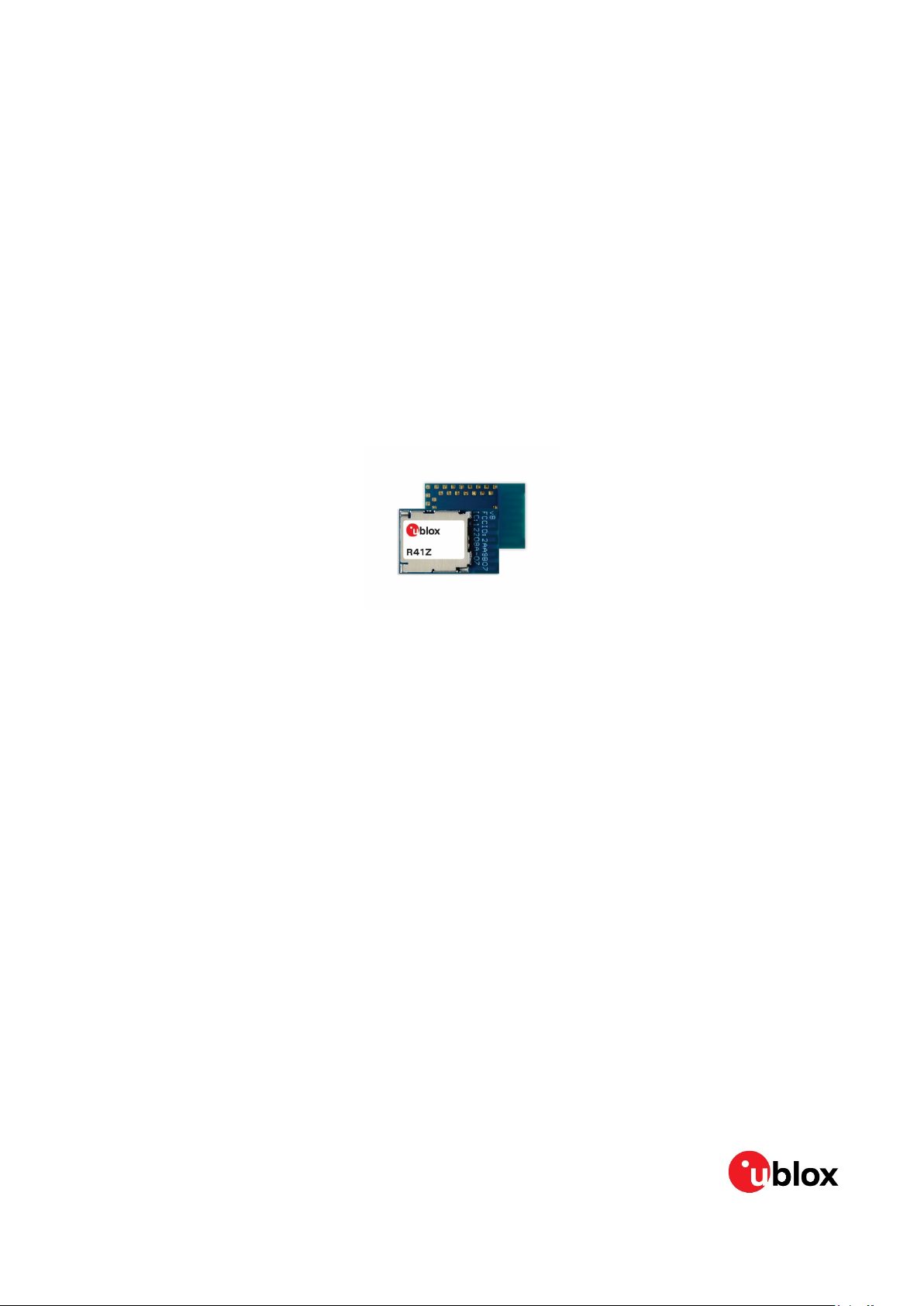
R41Z
Stand-alone Bluetooth 4.2 low energy and IEEE 802.15.4
module
Data sheet
This technical data sheet describes the R41Z stand-alone Bluetooth® low energy and IEEE 802.15.4
module.
stack using the NXP MCUXpresso SDK and integrated development environment (IDE).
UBX-19033355 - R08
C1-Public www.u-blox.com
Page 2
R41Z - Data sheet
u-blox or third parties may hold intellectual property rights in the products, names, logos and designs included in this
document. Copying, reproduction, modification or disclosure to third parties of th
permitted with the express written permission of u
The information contained herein is provided “as is” and u
implied, is given, including b
purpose of the information. This document may be revised by u
documents, visit www.u
Copy
Document information
Title R41Z
Subtitle Stand-alone Bluetooth 4.2 low energy and IEEE 802.15.4 module
Document type Data sheet
Document number UBX-19033355
Revision and date R08 17-Feb-2021
Disclosure restriction C1-Public
Product status Corresponding content status
Functional sample Draft For functional testing. Revised and supplementary data will be published later.
In development /
Prototype
Engineering sample Advance information Data based on early testing. Revised and supplementary data will be published later.
Initial production Early production information Data from product verification. Revised and supplementary data may be published later.
Mass production /
End of life
Objective specification Target values. Revised and supplementary data will be published later.
Production information Document contains the final product specification.
This document applies to the following products:
Product name Type number IN / PCN reference Product status
R41Z R41Z-TA-R-00 N/A Initial production
R41Z R41Z-TA-R-10 UBX-20017684 Initial production
right © u-blox AG.
UBX-19033355 - R08 Document information Page 2 of 42
C1-Public
ut not limited to, with respect to the accuracy, correctness, reliability and fitness for a particular
-blox.com.
-blox.
-blox assumes no liability for its use. No warranty, either express or
-blox at any time without notice. For the most recent
is document or any part thereof is only
Page 3

R41Z - Data sheet
Contents
Document information ............................................................................................................................. 2
Contents ....................................................................................................................................................... 3
1 Functional description ....................................................................................................................... 6
1.1 Features ........................................................................................................................................................ 6
1.2 Applications ................................................................................................................................................. 6
1.3 Block diagram .............................................................................................................................................. 7
1.4 Product specifications ............................................................................................................................... 7
2 Pin definition......................................................................................................................................... 9
2.1 Pin assignment ............................................................................................................................................ 9
2.1.1 Reference ........................................................................................................................................... 10
2.1.2 Power ................................................................................................................................................... 10
2.2 GPIO and LLWU signals ........................................................................................................................... 11
2.3 UART signals .............................................................................................................................................. 11
2.4 SPI signals .................................................................................................................................................. 12
2.5 I2C signals .................................................................................................................................................. 12
2.6 Touch sensing input (TSI) signals ......................................................................................................... 13
2.7 Timer/PWM module (TPM) signals ....................................................................................................... 13
2.8 Radio signals .............................................................................................................................................. 14
2.8.1 Wi-Fi/Bluetooth low energy coexistence signals ........................................................................ 14
2.8.2 Direct test mode (DTM) signals ..................................................................................................... 14
2.8.3 IEEE 802.15.4 Bit streaming mode (BSM) signals .................................................................... 14
2.9 Carrier modulator timer (CMT) signal ................................................................................................... 14
2.10 Single wire debug (SWD) and reset signals ......................................................................................... 14
2.11 RTC and clock signals .............................................................................................................................. 15
2.12 Analog signals ............................................................................................................................................ 15
3 Electrical specifications ................................................................................................................. 16
3.1 Absolute maximum ratings .................................................................................................................... 16
3.2 Operating conditions ................................................................................................................................ 16
3.3 DCDC converter operation ...................................................................................................................... 17
3.3.1 DCDC bypass mode .......................................................................................................................... 17
3.3.2 DCDC buck mode .............................................................................................................................. 18
3.3.3 DCDC boost mode ............................................................................................................................. 19
3.4 General purpose I/O and ports ................................................................................................................ 21
3.5 Analog I/O and VREF ................................................................................................................................ 21
3.5.1 Analog signals ................................................................................................................................... 21
3.5.2 VDDA and VREF ................................................................................................................................ 22
3.6 Module reset .............................................................................................................................................. 22
3.7 Debug and programming ......................................................................................................................... 22
3.8 Clocks .......................................................................................................................................................... 22
3.8.1 General parameters.......................................................................................................................... 22
UBX-19033355 - R08 Contents Page 3 of 42
C1-Public
Page 4

R41Z - Data sheet
3.8.2 Low frequency crystal ...................................................................................................................... 23
4 Firmware ............................................................................................................................................. 24
4.1 Factory image ............................................................................................................................................ 24
4.2 Bluetooth device address ........................................................................................................................ 24
5 Mechanical specifications ............................................................................................................. 25
5.1 Dimensions ................................................................................................................................................. 25
5.2 Recommended PCB land pads ............................................................................................................... 25
5.3 Module marking ......................................................................................................................................... 26
5.3.1 Module marking for type number R41Z-TA-R-00 ...................................................................... 26
5.3.2 Module marking for type number R41Z-TA-R-10 ...................................................................... 27
6 RF design notes ................................................................................................................................ 28
6.1 Recommended RF layout and ground plane ........................................................................................ 28
6.2 Mechanical enclosure ............................................................................................................................... 28
6.3 Antenna patterns ...................................................................................................................................... 29
6.3.1 X-Y plane ............................................................................................................................................. 29
6.3.2 Y-Z plane ............................................................................................................................................ 30
6.3.3 X-Z plane ............................................................................................................................................. 30
7 Evaluation development kit .......................................................................................................... 31
8 Qualification and approvals .......................................................................................................... 32
8.1 United States (FCC): ................................................................................................................................ 32
8.1.1 Labeling and user information requirements ............................................................................. 32
8.1.2 RF exposure ....................................................................................................................................... 33
8.2 Canada (ISED) ............................................................................................................................................ 33
8.2.1 Labeling and user information requirements ............................................................................. 33
8.2.2 RF exposure ....................................................................................................................................... 34
8.3 European Union regulatory compliance ............................................................................................... 34
8.3.1 Radio Equipment Directive (RED) 2014/53/EU .......................................................................... 34
8.4 Australia / New Zealand (RCM) .............................................................................................................. 34
8.5 Japan (MIC) ................................................................................................................................................ 34
8.6 Bluetooth qualification ............................................................................................................................. 35
9 Environmental ................................................................................................................................... 36
9.1 RoHS ............................................................................................................................................................ 36
9.2 REACH ......................................................................................................................................................... 36
9.3 California proposition 65 (P65) .............................................................................................................. 36
10 Product handling .............................................................................................................................. 37
10.1 Packaging ................................................................................................................................................... 37
10.2 Reel packaging ........................................................................................................................................... 37
10.3 Carrier tape dimensions for type number R41Z-TA-R-00 ................................................................ 37
10.4 Carrier tape dimensions for type number R41Z-TA-R-10 ................................................................ 38
10.5 Moisture sensitivity level ......................................................................................................................... 38
10.6 Reflow soldering ........................................................................................................................................ 38
11 Ordering information ...................................................................................................................... 39
UBX-19033355 - R08 Contents Page 4 of 42
C1-Public
Page 5

R41Z - Data sheet
12 Life support and other high-risk use warnings ....................................................................... 40
Related documents ................................................................................................................................ 41
Revision history ....................................................................................................................................... 41
Contact ....................................................................................................................................................... 42
UBX-19033355 - R08 Contents Page 5 of 42
C1-Public
Page 6

R41Z - Data sheet
1 Functional description
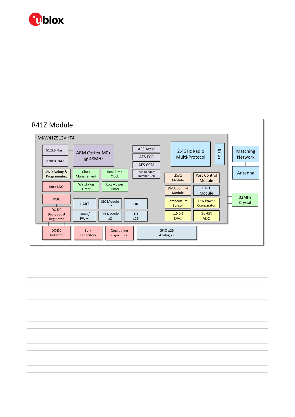
The R41Z module from u-blox is a highly integrated, ultra-low power module that enables Bluetooth
low energy and IEEE 802.15.4 connectivity based on the Kinetis KW41Z SoC from NXP
Semiconductors. With an ARM® Cortex™ M0+ processor, embedded 2.4 GHz transceiver supporting
FSK/GFSK and O-QPSK modulations, and integrated antenna, the R41Z provides a complete RF
solution with no additional RF design allowing faster time to market. Equipped with the ability to
concurrently communicate over Bluetooth, Thread, and Zigbee connections, the R41Z offers an
unprecedented level of connectivity in a single module. With an internal DC-DC Converter and a wide
supply voltage range of 0.9 V to 4.2 V, the R41Z can be directly powered by sources ranging from a
single alkaline cell to lithium polymer batteries.
1.1 Features
• Based on the NXP Kinetis KW41Z SoC
• Complete RF solution with an integrated DC-DC converter
• Bluetooth 4.2 1M PHY
• IEEE 802.15.4 with Thread and Zigbee support
• ARM® Cortex™-M0+ 32-bit processor
• Serial Wire Debug (SWD)
• Over-the-Air (OTA) firmware updates
• 512 KB embedded flash memory
• 128 KB RAM
• 25 GPIO, 2 dedicated analog pins
• 16-bit / 500KSPS ADC
• 12-bit DAC
• – 40 °C to +85 °C temperature range
• 16 capacitive touch sensing Inputs
• Two SPI master/slave (12 Mbps)
• Two I2C master/slave
• UART (w/ CTS/RTS and DMA)
• Low power comparator
• Temperature sensor
• Infrared communication interface
• Nine low power modes
• True random number generator
• 128-bit AES HW encryption
• 32-bit Real-Time Clock (RTC)
• Wi-Fi coexistence support
• Dimensions: 10.6 x 16.2 x 2.0 mm
1.2 Applications
• Beacons – iBeacon™, Eddystone, AltBeacon, and so on.
• Low-power sensors
• Fitness devices
• Wearables
• Climate control
• Lighting
• Safety and security
• Home appliances
• Access control
UBX-19033355 - R08 Functional description Page 6 of 42
C1-Public
Page 7
R41Z - Data sheet
• Internet of Things
• Home health care
• Advanced remote controls
• Smart energy management
• Low-power sensor Networks
• Interactive entertainment
• Key fobs
• Environmental monitoring
• Hotel automation
• Office automation
1.3 Block diagram
Figure 1: Block diagram of R41Z
1.4 Product specifications
Detail Description
Bluetooth
Bluetooth version Bluetooth 4.2
Security AES-128
LE connections 2
Thread / Zigbee
Version Thread 1.1, Zigbee 3.0
Stack NXP KW41Z Thread stack, NXP KW41Z Zigbee stack
Security AES-128
Radio
Frequency 2.360 GHz to 2.483 GHz
Modulations GFSK at 1 Mbps, OQPSK @ 250 Kbps
Transmit power +3.5 dBm
Receiver sensitivity – 95 dBm (Bluetooth low energy), – 100 dBm (IEEE 802.15.4)
Antenna Integrated (-1 dBi peak)
UBX-19033355 - R08 Functional description Page 7 of 42
C1-Public
Page 8

R41Z - Data sheet
Detail Description
Current consumption
TX only @ 0 dBm, bypass mode 14.7 mA
TX only @ 0 dBm, DCDC enabled,
3.6 V Vin
RX only bypass mode 16.2 mA
RX only, DCDC enabled, 3.6 Vin 6.7 mA
Normal Run CPU @ 48 MHz @ 3.0 V,
DCDC enabled
Very-Low-Power Run CPU @ 4 MHz
@ 3.0 V, DCDC enabled
Very-Low-Leakage Stop 3 (RAM
retained) @ 3.0 V @ 25 °C, DCDC
enabled
Very-Low-Leakage Stop 0 @ 3.0 V
@25 °C, bypass mode
Dimensions
R41Z Length: 16.2 mm ± 0.3 mm
Width: 10.6 mm ± 0.3 mm
Height: 2.0 mm ± 0.1 mm
Hardware
Interfaces SPI Master/Slave x 2
Power supply Boost mode: 0.9 V to 1.8 V, 1.1 V required to startup
Temperature range -40 °C to +85 °C
Certifications
USA (FCC) FCC part 15 modular certification
Canada (ISED) Industry Canada RSS-210 modular certification
Europe (CE) EN 62368-1:2014+A11:2017: Health and Safety of the User
Japan (MIC) Ministry of Internal Affairs and Communications (MIC) of Japan pursuant to the Radio
Australia / New Zealand (RCM)
Bluetooth
Radio chip
NXP KW41Z Additional details: MKW41Z Data Sheet Software & Tools
6.1 mA
4.8 mA
137 µA
1.8 µA
182 nA
UART x 1
Touch Sense Interface x 16
Two-Wire Master/Slave (I2C) x2
GPIO x 25
Analog input x 6
Bypass mode: 1.71 V to 3.6 V
Buck mode: 1.8 V to 4.2 V, 2.1 V required to startup
FCC ID: 2AA9B07
IC: 12208A-07
EN 301 489-1 V2.1.1 & 3.1 (b): Electromagnetic Compatibility
EN 301 489-17 V3.1.1
EN 300 328 V2.1.1 3.2: Effective use of spectrum allocated
Act of Japan
MIC: 210-109448
AS/NZS 4268:2017, Radio equipment and systems – Short range devices
RF-PHY Component (Tested) – DID: D035037; QDID: 95459
UBX-19033355 - R08 Functional description Page 8 of 42
C1-Public
Page 9
R41Z - Data sheet
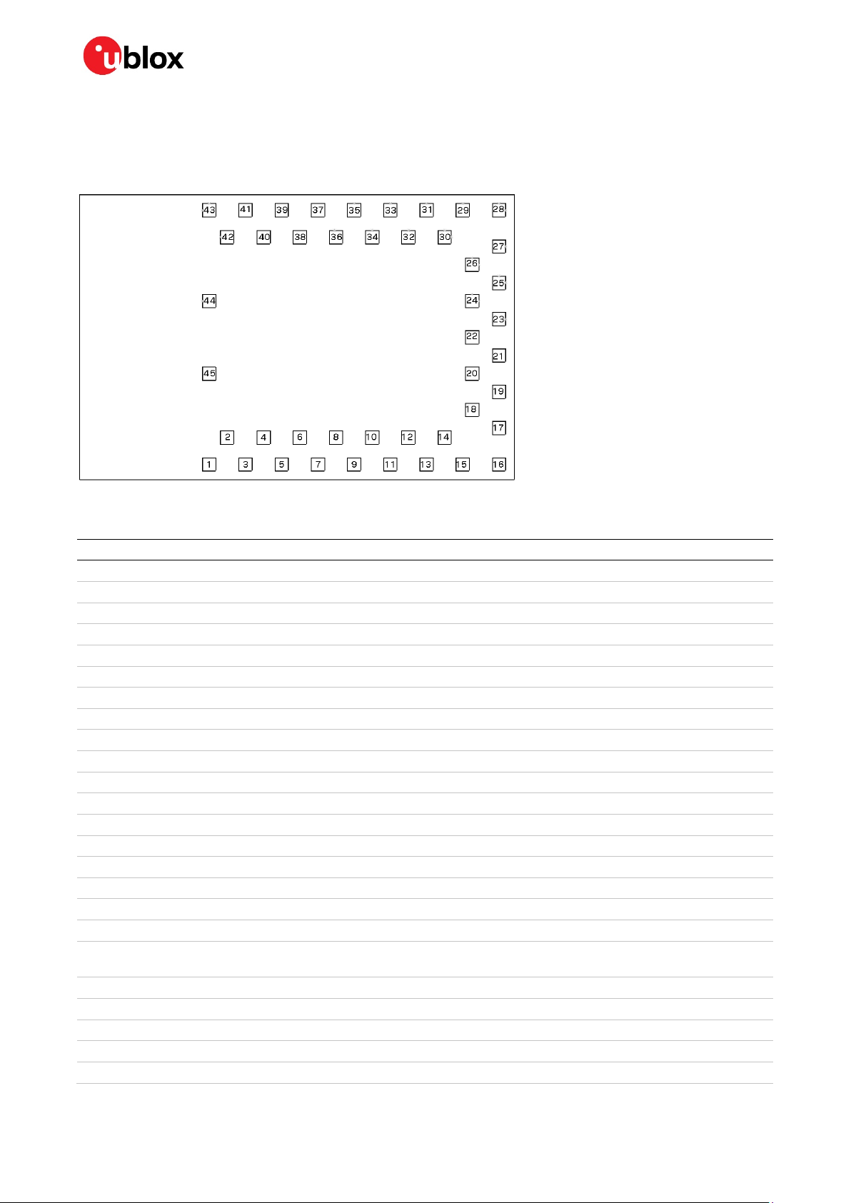
2 Pin definition
2.1 Pin assignment
Figure 2: R41Z pin assignment
Pin Name Direction Description Default State at POR KW41Z pin Remarks
2 PTC1 I/O GPIO Disabled PTC1
3 PTC2 I/O GPIO Disabled PTC2
4 PTC3 I/O GPIO Disabled PTC3
5 PTC4 I/O GPIO Disabled PTC4
6 PTC5 I/O GPIO Disabled PTC5
7 PTC6 I/O GPIO Disabled PTC6
8 PTC7 I/O GPIO Disabled PTC7
10 PTC16 I/O GPIO Disabled PTC16
11 PTC17 I/O GPIO Disabled PTC17
12 PTC18 I/O GPIO Disabled PTC18
13 PTC19 I/O GPIO Disabled PTC19
14 PTA0 I/O GPIO SWDIO, Pullup EN PTA0
15 PTA1 I/O GPIO SWCLK, Pulldown EN PTA1
17 PTA2 I/O GPIO Reset, Pullup EN PTA2
18 PTA16 I/O GPIO Disabled PTA16
19 PTA17 I/O GPIO Disabled PTA17
20 PTA18 I/O GPIO Disabled PTA18
21 PTA19 I/O GPIO Disabled PTA19
30 PTB0 I/O GPIO XTAL_OUT_EN
31 PTB1 I/O GPIO Disabled PTB1
32 PTB2 I/O GPIO Disabled PTB2
33 PTB3 I/O GPIO Disabled PTB3
34 PTB16 I/O GPIO EXTAL32K PTB16
36 PTB17 I/O GPIO XTAL32K PTB17
PTB0 See e10224 in NXP
KW41Z errata
UBX-19033355 - R08 Pin definition Page 9 of 42
C1-Public
Page 10
R41Z - Data sheet
ADC/Comparator
ADC/Comparator
Pin Name Direction Description Default State at POR KW41Z pin Remarks
37 PTB18 I/O GPIO Non-maskable
Interrupt req
38 ADC0_P In
input
39 ADC0_N In
input
Table 1: R41Z GPIO / Analog pin-out
N/A ADC0_P
N/A ADC0_N
PTB18
2.1.1 Reference
Pin Name Direction Description Remarks
40 XTAL_OUT Out 32 MHz Clock output
41 VREF I/O Analog reference voltage. Internally or
externally sourced
42 VDDA Power Analog supply. Internally sourced VDDA is connected to V1P8 through a
Table 2: Pin descriptions – Reference
power filtering circuit on the module
2.1.2 Power
Pin Name Direction Description Remarks
1 GND Power Electrical Ground
9 GND Power Electrical Ground
16 GND Power Electrical Ground
22 PSWITCH Input DCDC start signal
23 DCDC_CFG Input DCDC mode
24 GND Power Electrical Ground
25 VCC Power DCDC input
26 DCDC_LP Power DCDC signal
27 V1P8 Power DCDC IO and peripheral voltage
28 GND Power Electrical Ground
29 V1P5 Power DCDC RF supply See the DCDC converter operation
35 GND Power Electrical Ground
43 GND Power Electrical Ground
44 GND Power Electrical Ground
45 GND Power Electrical Ground
Table 3: Power
See the DCDC converter operation
section for details on signal usage
and DCDC modes
section for details on signal usage
and DCDC modes
☞ Internal peripherals on the R41Z (such as UART and I2C) can be routed to multiple pin options
using multiplexing. However, each pin can only be used with certain peripherals. See the following
sections for details on which pins can be used for a given function.
☞ Signal options for a pin are selected using a pin mux value. On many pins, there are multiple signals
UBX-19033355 - R08 Pin definition Page 10 of 42
C1-Public
that are accessed with the same pin mux value. See the
details on configuring these functions.
NXP KW41Z Reference Manual for
Page 11

R41Z - Data sheet
2.2 GPIO and LLWU signals
To use a Pin as GPIO or as a Low Leakage Wake-Up source, use pin mux ALT1. The LLWU pins can be
used to trigger interrupts that can bring the module out of Low Leakage sleep modes.
Signal Direction Description Pin Port Mux Alt Remarks
PTC1 I/O GPIO 2 PTC1 ALT1
PTC2 / LLWU_P10 I/O GPIO, LLWU 3 PTC2 ALT1
PTC3 / LLWU_P11 I/O GPIO, LLWU 4 PTC3 ALT1
PTC4 / LLWU_P12 I/O GPIO, LLWU 5 PTC4 ALT1
PTC5 / LLWU_P13 I/O GPIO, LLWU 6 PTC5 ALT1
PTC6 / LLWU_P14 I/O GPIO, LLWU 7 PTC6 ALT1
PTC7 / LLWU_P15 I/O GPIO, LLWU 8 PTC7 ALT1
PTC16 / LLWU_P0 I/O GPIO, LLWU 10 PTC16 ALT1
PTC17 / LLWU_P1 I/O GPIO, LLWU 11 PTC17 ALT1
PTC18 / LLWU_P2 I/O GPIO, LLWU 12 PTC18 ALT1
PTC19 / LLWU_P3 I/O GPIO, LLWU 13 PTC19 ALT1
PTA0 I/O GPIO 14 PTA0 ALT1
PTA1 I/O GPIO 15 PTA1 ALT1
PTA2 I/O GPIO 17 PTA2 ALT1
PTA16 / LLWU_P4 I/O GPIO, LLWU 18 PTA16 ALT1
PTA17 / LLWU_P5 I/O GPIO, LLWU 19 PTA17 ALT1
PTA18 / LLWU_P6 I/O GPIO, LLWU 20 PTA18 ALT1
PTA19 / LLWU_P7 I/O GPIO, LLWU 21 PTA19 ALT1
PTB0 / LLWU_P8 I/O GPIO, LLWU
PTB1 I/O GPIO 31 PTB1 ALT1
PTB2 I/O GPIO 32 PTB2 ALT1
PTB3 I/O GPIO 33 PTB3 ALT1
PTB16 I/O GPIO 34 PTB16 ALT1
PTB17 I/O GPIO 36 PTB17 ALT1
PTB18 I/O GPIO 37 PTB18 ALT1
Table 4: GPIO and LLWU signal map
30 PTB0 ALT1 See e10224 in
NXP KW41Z errata
2.3 UART signals
Signal Direction Description Pin Port Mux Alt
LPUART0_RX In UART Data Receiver 3
LPUART0_TX Out UART Data Transmit 4
LPUART0_CTS_b In UART Clear to Send 5
LPUART0_RTS_b Out UART Request to Send 2
Table 5: UART signal map
UBX-19033355 - R08 Pin definition Page 11 of 42
C1-Public
7
11
8
12
13
6
10
PTC2
PTC6
PTC17
PTC3
PTC7
PTC18
PTC4
PTC19
PTC1
PTC5
PTC16
ALT4
ALT4
ALT4
ALT4
ALT4
ALT4
ALT4
ALT4
ALT4
ALT4
ALT4
Page 12

R41Z - Data sheet
2.4 SPI signals
Signal Direction Description Pin Port Mux Alt
SPI0_SCK I/O SPI0 Clock 10 PTC16 ALT2
SPI0_SOUT Out SPI0 Serial Out 11 PTC17 ALT2
SPI0_SIN In SPI0 Serial In 12 PTC18 ALT2
SPI0_PCS0 I/O SPI0 Chip Select / Slave Select 0 13 PTC19 ALT2
SPI0_PCS1 I/O SPI0 Chip Select / Slave Select 1 14 PTA0 ALT2
SPI0_PCS2 I/O SPI0 Chip Select / Slave Select 2 8 PTC7 ALT2
SPI1_SCK I/O SPI1 Clock 20 PTA18 ALT2
SPI1_SOUT Out SPI1 Serial Out 18 PTA16 ALT2
SPI1_SIN In SPI1 Serial In 19 PTA17 ALT2
SPI1_PCS0 I/O SPI1 Chip Select / Slave Select 0 15
21
Table 6: SPI signal map
PTA1
PTA19
ALT2
ALT2
2.5 I2C signals
Signal Direction Description Pin Port Mux Alt
I2C0_SDA I/O I2C0 Serial Data Line 2
10
31
I2C0_SCL I/O I2C0 Serial Clock Line 13
30
I2C1_SDA I/O I2C1 Serial Data Line 4
8
12
36
I2C1_SCL I/O I2C1 Serial Clock Line 3
7
11
34
37
Table 7: I2C signal map
PTC1
PTC16
PTB1
PTC19
PTB0
PTC3
PTC7
PTC18
PTB17
PTC2
PTC6
PTC17
PTB16
PTB18
ALT3
ALT3
ALT3
ALT3
ALT3
ALT3
ALT3
ALT3
ALT3
ALT3
ALT3
ALT3
ALT3
ALT3
UBX-19033355 - R08 Pin definition Page 12 of 42
C1-Public
Page 13

R41Z - Data sheet
2.6 Touch sensing input (TSI) signals
TSI signals are the inputs used by the R41Z’s capacitive touch sensing system. See NXP Application
Note AN3863 for electrical and PCB layout recommendations.
Signal Direction Description Pin Port Mux Alt
TSI0_CH0 In TSI0 channel 0 5 PTC4 ALT0
TSI0_CH1 In TSI0 channel 1 6 PTC5 ALT0
TSI0_CH2 In TSI0 channel 2 7 PTC6 ALT0
TSI0_CH3 In TSI0 channel 3 8 PTC7 ALT0
TSI0_CH4 In TSI0 channel 4 10 PTC16 ALT0
TSI0_CH5 In TSI0 channel 5 11 PTC17 ALT0
TSI0_CH6 In TSI0 channel 6 12 PTC18 ALT0
TSI0_CH7 In TSI0 channel 7 13 PTC19 ALT0
TSI0_CH8 In TSI0 channel 8 14 PTA0 ALT0
TSI0_CH9 In TSI0 channel 9 15 PTA1 ALT0
TSI0_CH10 In TSI0 channel 10 18 PTA16 ALT0
TSI0_CH11 In TSI0 channel 11 19 PTA17 ALT0
TSI0_CH12 In TSI0 channel 12 20 PTA18 ALT0
TSI0_CH13 In TSI0 channel 13 21 PTA19 ALT0
TSI0_CH14 In TSI0 channel 14 3 PTC2 ALT0
TSI0_CH15 In TSI0 channel 15 4 PTC3 ALT0
Table 8: TSI signal map
2.7 Timer/PWM module (TPM) signals
Signal Direction Description Pin Port Mux Alt
TPM0_CH0 I/O TPM0 channel 0 18
TPM0_CH1 I/O TPM0 channel 1 4
TPM0_CH2 I/O TPM0 channel 2 2
TPM0_CH3 I/O TPM0 channel 3 10
TPM1_CH0 I/O TPM1 channel 0 5
TPM1_CH1 I/O TPM1 channel 1 6
TPM2_CH0 I/O TPM2 channel 0 7
TPM2_CH1 I/O TPM2 channel 1 8
TPM_CLKIN1 In TPM external clock signal 19 PTA17 ALT5
EXTRG_IN In TPM/ADC External Trigger signal 5 PTC4 ALT3
Table 9: TPM signal map
37
30
31
17
14
32
15
33
20
34
21
36
PTA16
PTB18
PTC3
PTB0
PTC1
PTB1
PTC16
PTA2
PTC4
PTA0
PTB2
PTC5
PTA1
PTB3
PTC6
PTA18
PTB16
PTC7
PTA19
PTB17
ALT5
ALT5
ALT5
ALT5
ALT5
ALT5
ALT5
ALT5
ALT5
ALT5
ALT5
ALT5
ALT5
ALT5
ALT5
ALT5
ALT5
ALT5
ALT5
ALT5
UBX-19033355 - R08 Pin definition Page 13 of 42
C1-Public
Page 14

R41Z - Data sheet
2.8 Radio signals
2.8.1 Wi-Fi/Bluetooth low energy coexistence signals
Signal Direction Description Pin Port Mux Alt
BLE_RF_ACTIVE Out External radio disable signal 2
13
RF_NOT_ALLOWED In R41Z radio disable signal 6
32
Table 10: Wi-Fi/Bluetooth LE Coexistence signal map
2.8.2 Direct test mode (DTM) signals
Signal Direction Description Pin Port Mux Alt
DTM_RX In Direct Test Mode receive signal 3
11
31
DTM_TX Out Direct Test Mode transmit signal 4
12
32
RF_RESET In Radio reset signal 19 PTA17 ALT1
Table 11: DTM signals
PTC1
PTC19
PTC5
PTB2
PTC2
PTC17
PTB1
PTC3
PTC18
PTB2
ALT7
ALT7
ALT2
ALT2
ALT7
ALT7
ALT2
ALT7
ALT7
ALT3
2.8.3 IEEE 802.15.4 Bit streaming mode (BSM) signals
Signal Direction Description Pin Port Mux Alt
BSM_DATA I/O Bit Streaming Mode Data signal 5
8
12
BSM_CLK Out Bit Streaming Mode clock signal 6
13
36
BSM_FRAME Out Bit Streaming Mode Frame signal 7
11
Table 12: BSM signal map
PTC4
PTC7
PTC18
PTC5
PTC19
PTB17
PTC6
PTC17
ALT7
ALT7
ALT5
ALT7
ALT5
ALT7
ALT7
ALT5
2.9 Carrier modulator timer (CMT) signal
Signal Direction Description Pin Port Mux Alt
CMT_IRO Out Carrier Modulator Timer out
signal
Table 13: CMT signal map
3
30
PTC2
PTB0
ALT5
ALT7
2.10 Single wire debug (SWD) and reset signals
Signal Direction Description Pin Port Mux Alt
SWD_DIO I/O SWD data signal 14 PTA0 ALT7
SWD_CLK In SWD clock signal 15 PTA1 ALT7
RESET_b I/O System reset signal, bidirectional 17 PTA2 ALT7
Table 14: SWD and reset signals
UBX-19033355 - R08 Pin definition Page 14 of 42
C1-Public
Page 15

R41Z - Data sheet
2.11 RTC and clock signals
Signal Direction Description Pin Port Mux Alt Remarks
XTAL_OUT_EN In EN input for XTAL_OUT (Pin 40) 7
30
CLKOUT Out Internal clocks monitor 30
33
RTC_CLKOUT Out RTC 1 Hz clock signal 33 PTB3 ALT7
EXTAL32K In 32 kHz external clock/oscillator 34 PTB16 ALT0
XTAL32K In 32 kHz external clock 36 PTB17 ALT0
Table 15: RTC and clock signal map
PTC6
PTB01
PTB0
PTB3
ALT1
ALT1
ALT7
ALT4
See e10224 in NXP
KW41Z errata
2.12 Analog signals
Signal Direction Description Pin Port Mux Alt
CMP0_OUT Out Comparator 0 output 30 PTB0 ALT4
CMP0_IN0 In Comparator 0 Single-ended
input 0
CMP0_IN1 In Comparator 0 Single-ended
input 1
CMP0_IN2 In Comparator 0 Single-ended
input 2
CMP0_IN3 In Comparator 0 Single-ended
input 3
CMP0_IN4 In Comparator 0 Single-ended
input 4
CMP0_IN5 In Comparator 0 Single-ended
input 5
ADC0_SE0 In ADC Channel 0 Single-ended
input 0
ADC0_SE1 In ADC Channel 0 Single-ended
input 1
ADC0_SE2 In ADC Channel 0 Single-ended
input 2
ADC0_SE3 In ADC Channel 0 Single-ended
input 3
ADC0_SE4 In ADC Channel 0 Single-ended
input 4
ADC0_DP0 In ADC Channel 0 Differential input
positive
ADC0_DN0 In ADC Channel 0 Differential input
negative
DAC0_OUT Out DAC Channel 0 Single-ended
output
Table 16: Analog signals
38 - -
39 - -
37 PTB18 ALT0
32 PTB2 ALT0
33 PTB3 ALT0
31 PTB1 ALT0
31 PTB1 ALT0
33 PTB3 ALT0
32 PTB2 ALT0
37 PTB18 ALT0
21 PTA19 ALT0
38 - -
39 - -
37 PTB18 ALT0
UBX-19033355 - R08 Pin definition Page 15 of 42
C1-Public
Page 16

R41Z - Data sheet
3 Electrical specifications
⚠ Stressing the device above one or more of the ratings listed in the Absolute maximum rating
section may cause permanent damage. These are stress ratings only. Operating the module at
these or at any conditions other than those specified in the Operating conditions section of this
document should be avoided. Exposure to absolute maximum rating conditions for extended
periods may affect device reliability.
☞ Operating condition ranges define those limits within which the functionality of the device is
guaranteed. Where application information is given, it is advisory only and does not form part of
the specification.
3.1 Absolute maximum ratings
Symbol Description Condition Min Max Unit
V
Voltage on supply pin DCDC Boost Mode
CC_MAX
DCDC Bypass Mode
DCDC Buck Mode
V
Voltage on V1P8 and GPIO pins All DCDC modes –0.3 3.6 V
1P8_MAX
V
Voltage on V1P5 All DCDC modes –0.3 3.6 V
RF_MAX
TS Storage Temperature - –40 125 °C
Table 17: Absolute maximum ratings
–0.3
–0.3
–0.3
1.8
3.6
4.2
V
V
V
⚠ The product is not protected against overvoltage or reversed voltages. If necessary, voltage spikes
exceeding the power supply voltage specification, given in table above, must be limited to values
within the specified boundaries by using appropriate protection devices.
3.2 Operating conditions
☞ Unless otherwise specified, all operating condition specifications are at an ambient temperature
of 25 °C and a supply voltage of 3.0 V.
⚠ Operation beyond the specified operating conditions is not recommended and extended exposure
beyond them may affect device reliability.
Symbol Parameter Condition Min. Typ. Max. Unit
V
cc
V
1P8
V
RF
I
1P8
T
A
Figure 3: Operating conditions
Voltage on Supply Pin DCDC Boost Mode
Voltage on V1P8 and
GPIO
Voltage on V1P5 All DCDC modes 1.8 3.3 3.6 V
V1P8 output current DCDC Buck Mode,
Ambient Temperature - –40 25 85 °C
DCDC Bypass Mode
DCDC Buck Mode
All DCDC modes 1.45 3.3 3.6 V
1.8 Vout
DCDC Buck Mode,
3.0 Vout
DCDC Boost Mode, 1.7 Vin, 1.8 Vout
DCDC Boost Mode,
0.9 Vin, 3.0Vout
0.9
1.71
1.8
-
-
-
-
1
2
1.5
3.3
3.3
-
-
-
-
1.8
3.6
4.2
45
27
45
10
V
V
V
mA
mA
mA
mA
UBX-19033355 - R08 Electrical specifications Page 16 of 42
C1-Public
Page 17

R41Z - Data sheet
☞ 1: In Boost mode, a minimum of 1.1 V is required to start the DCDC converter. Once started, the
converter can operate at 0.9 V.
☞ 2: In Buck mode, a minimum of 2.1 V is required to start the DCDC converter.
3.3 DCDC converter operation
The R41Z module contains an integrated DCDC converter which allows for three modes of operation
without additional components. When operating in DCDC Buck mode, power consumption from using
the radio can be reduced compared to DCDC Bypass mode. DCDC Boost mode allows the use of a
single alkaline or other low voltage source. While it is possible to switch between these modes in a
single design, for example the R41Z Evaluation Board, it is not recommended to switch between
modes while power is applied.
3.3.1 DCDC bypass mode
Mode Pin Name Net connection
Bypass 22 PSWITCH Ground
23 DCDC_CFG 1.71 V - 3.6 V Source IN
25 VCC 1.71 V - 3.6 V Source IN
26 DCDC_LP No Connection
27 V1P8 1.71 V - 3.6 V Source IN
29 V1P5 1.45 V - 3.6 V Source IN
Table 18: Bypass mode pin connections
Figure 4: Schematic: DCDC bypass mode example
UBX-19033355 - R08 Electrical specifications Page 17 of 42
C1-Public
Page 18

R41Z - Data sheet
3.3.2 DCDC buck mode
Mode Pin Name Net Connection
Buck 22 PSWITCH
23 DCDC_CFG 1.8 V - 4.2 V Source IN
25 VCC 1.8 V - 4.2 V Source IN
26 DCDC_LP No Connection
27 V1P8 No Connection or 1.8 V – 3.0 V OUT
29 V1P5 No Connection
1
1.8 V - 4.2 V Source IN
2
☞ 1: In Buck mode, PSWITCH can inhibit the DCDC converter from starting when the source voltage is applied. When
PSWITCH is connected to the source voltage, the DCDC converter will start. Once started, PSWITCH can be reconnected
to GND without disrupting the DCDC converter’s operation.
☞ 2: V1P8 is the R41Z’s IO voltage when the DCDC converter is running in either Buck or Boost mode. V1P8 can source a
limited number of additional peripheral devices (sensors, LEDs, etc.) that connect directly to the R41Z’s IO. In Buck mode,
V1P8 cannot output a voltage greater than the source voltage.
Table 19: DCDC buck mode pin connections
Figure 5: Schematic: DCDC buck mode example
UBX-19033355 - R08 Electrical specifications Page 18 of 42
C1-Public
Page 19

R41Z - Data sheet
V1P8 is the R41Z’s IO voltage when the DCDC
converter is running in either Buck or Boost mode.
V1P8 can source a limited number of additional
.) that
Figure 6: Schematic: DCDC buck mode PSWITCH example
3.3.3 DCDC boost mode
Mode Pin Name Net Connection Remarks
Boost 22 PSWITCH 0.9 V – 1.8 V Source IN
23 DCDC_CFG Ground
25 VCC 0.9 V – 1.8 V Source IN
26 DCDC_LP 0.9 V – 1.8 V Source IN
27 V1P8 No Connection or 1.8 V – 3.0 V OUT
29 V1P5 No Connection
Table 20: DCDC boost mode pin connections
peripheral devices (sensors, LEDs, and so on
connect directly to the R41Z’s IO.
UBX-19033355 - R08 Electrical specifications Page 19 of 42
C1-Public
Page 20

R41Z - Data sheet
VCC →
PSWITCH
DCDC_CFG
Figure 7: Schematic: DCDC boost mode example
When using Boost Mode care should be taken to ensure that DCDC_LP (Pin 26) is connected to VCC
(Pin 25) with a trace wide enough to carry the full current expected to be drawn from the R41Z module
and any peripherals sourced by the module. The connection should also be as short as possible.
V1P8 →
DCDC_LP
Figure 8: PCB: Boost mode suggested layout
UBX-19033355 - R08 Electrical specifications Page 20 of 42
C1-Public
Page 21

R41Z - Data sheet
3.4 General purpose I/O and ports
The general-purpose I/O is organized as three ports (A, B, and C) that enable access and control to
each of the 25 available GPIO pins. Each GPIO can be configured individually through a Pin Control
Register (PCR) and Port Data Direction Register (PDDR) with the following available features:
• Input/output direction
• Output drive strength
• Internal pull-up and pull-down resistors
• Trigger interrupts and/or DMA from input
• Read and clear interrupt flags
• Enable passive input filter
• Fast/slow slew rate selection
• Control pin multiplexing to internal modules
To use a pin as GPIO set the Pin Mux Control field of the pin to ALT1 in the PCR. Ports must have their
clock source enabled in the System Clock Gating Control Register 5 (SIM_SCGC5) before accessing
any port registers. Attempting to access port registers without the port clock enabled will cause
program execution to immediately vector to the default exception handler. Disabling the clock to ports
that are not being used will reduce power consumption. Ports should be disabled before turning off
the clock.
Symbol Parameter Min Max Unit
VIH Input High Voltage, 2.7 V ≤ VIO ≤ 3.6 V
Input High Voltage, 1.7 V ≤ V
≤ 2.7 V
IO
VIL Input Low Voltage, 2.7 V ≤ VIO ≤ 3.6 V
Input Low Voltage, 1.7 V ≤ V
V
Input Hysteresis - 0.6 x VIO V
HYS
≤ 2.7 V
IO
0.7 x V
IO
0.75 x VIO
-
-
-
-
0.35 x V
0.3 x VIO
V
IO
V
VOH Output high voltage VIO – 0.5 - V
VOL Output low voltage - 0.5 V
RP Pull resistance 20 50 kΩ
Table 21: GPIO properties
3.5 Analog I/O and VREF
3.5.1 Analog signals
Symbol Parameter Min Typ. Max. Unit
V
DDA
V
REF_OUT
V
VREF externally sourced 1.13 V
REFH
V
ADIN
V
ACIN
V
ACIO
I
CMPHS
I
CMP current, Low-speed mode - - 20 µA
CMPLS
V
CMPH
V
CMPL
Table 22: Analog properties
Analog supply voltage - V
- V
1P8
VREF internally sourced, factory trim 1.190 1.1950 1.200 V
DDA
V
DDA
16-bit, differential mode GND - 31/32 × V
16-bit, All other modes GND - V
CMP/6-bit ADC analog input voltage GND – 0.3 - V
V
REFH
V
1P8
REFH
V
V
CMP/6-bit ADC analog input voltage offset - - 20 mV
CMP current, High-speed mode - - 200 µA
Comparator output high V
– 0.5 - - V
1P8
Comparator output low - - 0.5 V
UBX-19033355 - R08 Electrical specifications Page 21 of 42
C1-Public
Page 22

R41Z - Data sheet
3.5.2 VDDA and VREF
The source voltage for the analog sub-system, VDDA, is supplied by V1P8 through a filtering circuit
onboard the R41Z module. The voltage reference pin, VREF, has two sourcing options: internal or
external. When externally supplied, VREF should be referenced to VDDA. Internal VREF is provided by
a resistor trimmed circuit. For details on using the analog modules, see the KW41Z Data Sheet.
3.6 Module reset
Pin 17, PTA2, is used as an external reset source by default. This pin can be used for other functions,
such as GPIO, by setting the RESET_PIN_CFG option bit of the FTFA_FPORT register to 0. This bit is
retained through system resets and low power modes.
3.7 Debug and programming
The R41Z module supports the two pin Serial Wire Debug (SWD) interface and offers flexible
mechanisms for non-intrusive debugging of program code. Breakpoints, single stepping, and
instruction trace capture of code execution flow are part of this support. The R41Z also supports
Micro Trace Buffer (MTB) which provide lightweight program trace capabilities using system RAM.
SWD pins can be repurposed as additional GPIO by the application.
The R41Z module does not support resets through the SWD interface. Resets from programmers and
test fixtures must be asserted through the reset pin.
3.8 Clocks
3.8.1 General parameters
The R41Z requires two clocks: a high frequency clock and a low frequency clock.
The high frequency clock is provided on-module by a high accuracy 32 MHz crystal. The low frequency
clock is required for Real Time Clock (RTC) operation and radio Deep Sleep Mode (DSM). In most
applications, an external crystal oscillator is required to provide the low frequency clock.
For normal run modes, an internal oscillator can provide the low frequency clock. However, to make
full use of reduced power modes an external crystal must be present.
For most applications with the low frequency crystal, external capacitors are not required. Internal,
programmable capacitors are provided on the R41Z module. To maintain accurate time keeping,
these internal capacitors should be adjusted for the PCB’s and crystal’s characteristics during
hardware initialization. Internal capacitance can be configured in 2pF increments using the RTC_CR
configuration register.
An external clock source can be used in place of the low frequency crystal. In this case, the clock source
should be connected to the EXTAL32K pin (PTB16) and XTAL23K (PTB17) should be left
unconnected.
The R41Z’s internal 32MHz clock can be provided to other devices using the XTAL_OUT signal on pin
40. This clock output can be toggled via software or externally enabled with the XTAL_OUT_EN signal.
See section 2.10 for XTAL_OUT_EN signal mapping options.
UBX-19033355 - R08 Electrical specifications Page 22 of 42
C1-Public
Page 23

R41Z - Data sheet
±
±
3.8.2 Low frequency crystal
Symbol Parameter Typ. Max. Unit
F
F
C
Table 23: Low frequency crystal recommended specifications
Crystal frequency 32.768 - kHz
NOM_LFXO
TOL_LFXO_BLE
L_LFXO
Frequency tolerance, Bluetooth LE applications
Load capacitance 7 12.5 pF
20
250 ppm
Figure 9: Schematic: Low frequency crystal
UBX-19033355 - R08 Electrical specifications Page 23 of 42
C1-Public
Page 24

R41Z - Data sheet
4 Firmware
Projects for the R41Z should utilize the MCUXpresso SDK, IDE and other utilities provided by NXP
Semiconductors. This will allow access to the very latest Bluetooth support from NXP
Semiconductors and provide an ongoing path as new features are released.
4.1 Factory image
The R41Z module is not loaded with a factory firmware image and is assigned firmware code “00”.
This code is either marked or encoded within the 2D data matrix. See section 5.3 for details.
☞ When the R41Z does not have firmware loaded that can be executed out of Power-on Reset (POR),
the R41Z module re-asserts POR. This should be considered when connecting the R41Z to other
devices on a shared reset circuit.
4.2 Bluetooth device address
The R41Z module is assigned a unique public Bluetooth device address that consists of the IEEE
Organizationally Unique Identifier (OUI) combined with six unique hexadecimal digits. The entire
Bluetooth device address is encoded within a 2D data matrix and the last six digits in human-readable
text printed on the module label, as described in section 5.3.
☞ This value is not pre-programmed into flash. The Bluetooth device address is typically located in
flash as part of the firmware image and accessed as a global constant. The Bluetooth device
address is printed encoded within the 2D data matrix and human readable text on the top of the
module.
☞ When loading custom firmware to the module, the MAC address must be inserted into the image.
This can be done using a 2D barcode scanner and suitable factory programmer tools. When
loading a new application to the module, care should be taken to ensure the MAC address is not
overwritten.
UBX-19033355 - R08 Firmware Page 24 of 42
C1-Public
Page 25

R41Z - Data sheet
5 Mechanical specifications
5.1 Dimensions
Figure 10: Mechanical drawing
5.2 Recommended PCB land pads
Figure 11: Recommended PCB land pads
☞ The RF keep-out area extends vertically to the board edges
UBX-19033355 - R08 Mechanical specifications Page 25 of 42
C1-Public
Page 26

R41Z - Data sheet
5.3 Module marking
5.3.1 Module marking for type number R41Z-TA-R-00
1
2
3
4
5
Figure 12: Module marking for type number R41Z-TA-R-00
Reference Description
1 FCC ID (USA)
2 Firmware version (00 = no factory firmware loaded)
3 Data Matrix with unique serial number of six alphanumeric symbols, also in human-readable form. The full
Bluetooth address consists of the IEEE OUI (94:54:93) with the six symbols appended: Example value:
94:54:93:XX:YY:ZZ
4 MIC ID and Giteki mark (Japan)
5 ISED ID (Canada)
Table 24: Module marking for type number R41Z-TA-R-00
UBX-19033355 - R08 Mechanical specifications Page 26 of 42
C1-Public
Page 27

R41Z - Data sheet
5.3.2 Module marking for type number R41Z-TA-R-10
1
2
3
4
5
6a
6b
7
Figure 13: Module marking for type number R41Z-TA-R-10
Reference Description
1 FCC ID (USA)
2 ISED ID (Canada)
3 Product name
3 + 4 Type number
5 MIC (Japan) Giteki mark and Certification ID
6a Data Matrix with unique serial number of 19 alphanumeric symbols. The first 3 symbols represent module
type number unique to each module variant, the next 12 symbols represent the unique hexadecimal Bluetooth
device address of the module AABBCCDDEEFF, and the last 4 symbols represent the hardware and firmware
version encoded HHFF. The IEEE OUI is in the first three bytes of the Bluetooth device address (AABBCC) and
is one of the following values: D4:CA:6E, CC:F9:57, 60:09:C3, 6C:1D:EB. The remaining hexadecimal digits
(DDEEFF) are unique.
6b Second half of Bluetooth device address in human-readable format (DDEEFF above)
7 Date of production encoded YY/WW (year / week)
Table 25: Module marking for type number R41Z-TA-R-10
UBX-19033355 - R08 Mechanical specifications Page 27 of 42
C1-Public
Page 28

R41Z - Data sheet
6 RF design notes
6.1 Recommended RF layout and ground plane
The integrated antenna on the R41Z module requires a suitable ground plane to radiate effectively.
The module antenna has been tuned for having a PCB directly below with no copper or any other metal
present. The module should be placed at the edge of the PCB with the antenna edge facing out. For
best performance, the ground plane should be on the same layer as the module or as close as possible.
If this is not possible in a design, ground planes on multiple layers generously connected with vias may
also be used. Reduced ground plane size will result in reduced radio performance.
Figure 14: R41Z RF Example based on evaluation board
6.2 Mechanical enclosure
Care should be taken when designing and placing the module into an enclosure. Metal should be kept
clear from the antenna area, both above and below. Any metal around the module can decrease RF
performance.
The module is designed and tuned to be in free air. Any potting, epoxy fill, plastic over-molding, or
conformal coating can negatively impact RF performance and must be evaluated by the customer. If
potting must be used, the compound should have a low dielectric constant and should be designed
for use with 2.4 GHz RF electronics.
UBX-19033355 - R08 RF design notes Page 28 of 42
C1-Public
Page 29

R41Z - Data sheet
6.3 Antenna patterns
Antenna patterns are based on the R41Z evaluation kit with a ground plane size of
82 mm x 56 mm. The X-Y-Z orientation is shown in Figure 15:
Figure 15: X-Y-Z antenna orientation
6.3.1 X-Y plane
Figure 16: X-Y plane antenna pattern
UBX-19033355 - R08 RF design notes Page 29 of 42
C1-Public
Page 30

R41Z - Data sheet
6.3.2 Y-Z plane
Figure 17: Y-Z plane antenna pattern
6.3.3 X-Z plane
Figure 18: X-Z plane antenna pattern
UBX-19033355 - R08 RF design notes Page 30 of 42
C1-Public
Page 31

R41Z - Data sheet
7 Evaluation development kit
u-blox has developed a full featured evaluation board that provides on-board programming and
debugging, power, and virtual COM port over USB, 32.768 kHz crystal, Arduino style IO headers two
mechanical user buttons, two capacitive touch buttons, 3-axis accelerometer/magnetometer (I
and a 4 Mbit flash chip (SPI). The evaluation board also allows for easy use of all the R41Z’s DCDC
power modes and can be powered from an adjustable LDO regulator, CR2032 coin cell battery, or
through an external power header. Power consumption can be measured through onboard current
sensing resistors and headers.
2
C),
Figure 19: R41Z evaluation board
UBX-19033355 - R08 Evaluation development kit Page 31 of 42
C1-Public
Page 32

R41Z - Data sheet
8 Qualification and approvals
8.1 United States (FCC):
The R41Z module has received Federal Communications Commission (FCC) CFR47
Telecommunications, Part 15 Subpart C “Intentional Radiators” modular approval in accordance with
Parts 15.212 and 15.247. The modular approval allows the end user to integrate the module into a
finished product without obtaining subsequent and separate FCC approvals for intentional radiation,
provided no changes or modifications are made to the module circuitry. Changes or modifications
could void the user’s authority to operate the equipment. The end user must comply with all of the
instructions provided by the Grantee, which indicate installation and/or operating conditions
necessary for compliance.
The finished product is required to comply with all applicable FCC equipment authorizations
regulations, requirements and equipment functions not associated with the transmitter module
portion. For example, compliance must be demonstrated to regulations for other transmitter
components within the host product; to requirements for unintentional radiators (Part 15 Subpart B
“Unintentional Radiators”), such as digital devices, computer peripherals, radio receivers, etc.; and to
additional authorization requirements for the non-transmitter functions on the transmitter module
(that is, Verification, or Declaration of Conformity) (for example, transmitter modules may also
contain digital logic functions) as appropriate.
☞ Modification to this product will void the users’ authority to operate this equipment.
⚠ The OEM is still responsible for verifying end product compliance with FCC Part 15, subpart B
limits for unintentional radiators through an accredited test facility.
8.1.1 Labeling and user information requirements
The R41Z is assigned the FCC ID number: 2AA9B07
If the FCC ID is not visible when the module is installed inside another device, then the outside of the
finished product into which the module is installed must also display a label referring to the enclosed
module. This exterior label can use the following or similar wording:
Contains FCC ID: 2AA9B07
In addition to marking the product with the appropriate FCC ID, the end product shall bear the
following statement in a conspicuous location on the device (FCC Rules, Title 47, Subchapter A, Part
15, Subpart B, Chapter §15.19):
This device complies with part 15 of the FCC Rules. Operation is subject to the following two
conditions: (1) This device may not cause harmful interference, and (2) this device must
accept any interference received, including interference that may cause undesired operation.
When the device is so small or for such use that it is impracticable to label it with the statement
specified above in a font that is four-point or larger, and the device does not have a display that can
show electronic labeling, then the information required by this paragraph shall be placed in the user
manual and must also either be placed on the device packaging or on a removable label attached to
the device.
The user manual may also require specific information based on the digital device classification. Refer
to the FCC Rules, Title 47, Subchapter A, Part 15, Subpart B, Chapter §15.105 for specific wording of
these notices.
UBX-19033355 - R08 Qualification and approvals Page 32 of 42
C1-Public
Page 33

R41Z - Data sheet
8.1.2 RF exposure
All transmitters regulated by FCC must comply with RF exposure requirements. KDB 447498 General
RF Exposure Guidance provides guidance in determining whether proposed or existing transmitting
facilities, operations or devices comply with limits for human exposure to Radio Frequency (RF) fields
adopted by the Federal Communications Commission (FCC).
This module is approved for installation into mobile and/or portable host platforms and must not be
co-located or operating in conjunction with any other antenna or transmitter except in accordance
with FCC multi-transmitter guidelines. End users must be provided with transmitter operating
conditions for satisfying RF Exposure compliance.
8.2 Canada (ISED)
The R41Z module is certified for use in Canada under Innovation, Science and Economic Development
Canada (ISED) Radio Standards Specification (RSS) RSS-247 Issue 2 and RSSGen.
8.2.1 Labeling and user information requirements
The R41Z is assigned the IC ID number: 12208A-07
Labeling Requirements for the Host Device (from Section 3.2.1, RSS-Gen, Issue 3, December 2010):
The host device shall be properly labeled to identify the module within the host device. The Industry
Canada certification label of a module shall be clearly visible at all times when installed in the host
device, otherwise the host device must be labeled to display the Industry Canada certification number
of the module, preceded by the words “Contains transmitter module”, or the word “Contains”, or
similar wording expressing the same meaning, as follows:
Contains transmitter module IC: 12208A-07
User Manual Notice for License-Exempt Radio Apparatus (from Section 7.1.3 RSS-Gen, Issue 3,
December 2010): User manuals for license-exempt radio apparatus shall contain the following or
equivalent notice in a conspicuous location in the user manual or alternatively on the device or both:
This device complies with Industry Canada license exempt RSS standard(s). Operation is
subject to the following two conditions: (1) this device may not cause interference, and (2)
this device must accept any interference, including interference that may cause undesired
operation of the device.
Le présent appareil est conforme aux CNR d'Industrie Canada applicables aux appareils radio
exempts de licence. L'exploitation est autorisée aux deux conditions suivantes: (1) l'appareil
ne doit pas produire de brouillage, et (2) l'utilisateur de l'appareil doit accepter tout brouillage
radioélectrique subi, même si le brouillage est susceptible d'en compromettre le
fonctionnement.
Transmitter Antenna (from Section 7.1.2 RSS-Gen, Issue 3, December 2010): User manuals
for transmitters shall display the following notice in a conspicuous location:
Under Industry Canada regulations, this radio transmitter may only operate using an
antenna of a type and maximum (or lesser) gain approved for the transmitter by Industry
Canada. To reduce potential radio interference to other users, the antenna type and its gain
should be so chosen that the equivalent isotropically radiated power (e.i.r.p.) is not more than
that necessary for successful communication.
Conformément à la réglementation d'Industrie Canada, le présent émetteur radio peut
fonctionner avec une antenne d'un type et d'un gain maximal (ou inférieur) approuvé pour
l'émetteur par Industrie Canada. Dans le but de réduire les risques de brouillage
radioélectrique à l'intention des autres utilisateurs, il faut choisir le type d'antenne et son
gain de sorte que la puissance isotrope rayonnée équivalente (p.i.r.e.) ne dépasse pas
l'intensité nécessaire à l'établissement d'une communication satisfaisante.
UBX-19033355 - R08 Qualification and approvals Page 33 of 42
C1-Public
Page 34

R41Z - Data sheet
8.2.2 RF exposure
All transmitters regulated by IC must comply with RF exposure requirements listed in RSS-102 - Radio
Frequency (RF) Exposure Compliance of Radiocommunication Apparatus (All Frequency Bands). This
module is approved for installation into mobile and/or portable host platforms and must not be colocated or operating in conjunction with any other antenna or transmitter except in accordance with
Industry Canada's multi-transmitter guidelines. End users must be provided with transmitter
operating conditions for satisfying RF Exposure compliance.
8.3 European Union regulatory compliance
Information about regulatory compliance of the European Union for the R41Z module is available in
the R41Z Declaration of Conformity.
8.3.1 Radio Equipment Directive (RED) 2014/53/EU
The R41Z module complies with the essential requirements and other relevant provisions of Radio
Equipment Directive (RED) 2014/53/EU.
8.4 Australia / New Zealand (RCM)
The R41Z has been tested to comply with the AS/NZS 4268:2017, Radio equipment and systems –
Short range devices – Limits and methods of measurement. The report may be obtained from your
local FAE and may be used as evidence in obtaining permission to use the Regulatory Compliance
Mark (RCM).
Information on registration as a Responsible Party, license and labeling requirements may be found
at the following websites:
Australia: http://www.acma.gov.au/theACMA/radiocommunications-short-range-devices-standard-
2004
New Zealand: http://www.rsm.govt.nz/compliance
Only Australian-based and New Zealand-based companies who are registered may be granted
permission to use the RCM. An Australian-based or New Zealand-based agent or importer may also
register as a Responsible Party to use the RCM on behalf of a company not in Australia or New
Zealand.
8.5 Japan (MIC)
The R41Z module has received type certification and is labeled with its own technical conformity mark
and certification number as required to conform to the technical standards regulated by the Ministry
of Internal Affairs and Communications (MIC) of Japan pursuant to the Radio Act of Japan.
Integration of this module into a final end product does not require additional radio certification
provided installation instructions are followed and no modifications of the module are allowed.
Additional testing may be required:
• If the host product is subject to electrical appliance safety (for example, powered from an AC
mains), the host product may require Product Safety Electrical Appliance and Material (PSE)
testing. The integrator should contact their conformance laboratory to determine if this testing is
required.
• There is a voluntary Electromagnetic Compatibility (EMC) test for the host product administered
by VCCI: http://www.vcci.jp/vcci_e/index.html
The label on the end product which contains a R41Z module must follow the MIC marking
requirements. Labeling requirements for Japan available at the Ministry of Internal Affairs and
Communications (MIC) website:
UBX-19033355 - R08 Qualification and approvals Page 34 of 42
C1-Public
http://www.tele.soumu.go.jp/e/index.htm.
Page 35

R41Z - Data sheet
The R41Z module is labeled with its assigned technical conformity mark and certification number.
The end-product in which this module is being used must have an external label referring to the type
certified module inside:
Contains transmitter module with certificate number:
Figure 20: Japan MIC Mark
8.6 Bluetooth qualification
The Bluetooth SIG maintains the Bluetooth Specification, and ensures that products are properly
tested and comply with the Bluetooth license agreements. Companies that list products with the
Bluetooth SIG are required to be members of the SIG and submit the listed fees. Refer to this link for
details: https://www.bluetooth.com/develop-with-bluetooth/qualification-listing
The R41Z Bluetooth Low Energy module based on the NXP Semiconductors KS41Z is listed as a
“Tested Component” with QDID 95459. This allows an end-product based on a R41Z module to inherit
the component listings without the need to run through all of the tests again. The end-product will
often inherit several QDIDs that are identified on a “Declaration of Compliance”.
UBX-19033355 - R08 Qualification and approvals Page 35 of 42
C1-Public
Page 36

R41Z - Data sheet
9 Environmental
9.1 RoHS
The R41Z module is in compliance with Directive 2011/65/EU, 2015/863/EU of the European
Parliament and the Council on the restriction of the use of certain hazardous substances in electrical
and electronic equipment.
9.2 REACH
The R41Z module does not contain the SVHC (Substance of Very High Concern), as defined by
Directive EC/1907/2006 Article according to REACH Annex XVII.
9.3 California proposition 65 (P65)
This product can expose you to Nickel (metallic), which is known to the State of California to cause
cancer. For more information go to www.P65Warnings.ca.gov.
☞ Warnings are not required where the listed chemical is inaccessible to the average user of the
end product.
UBX-19033355 - R08 Environmental Page 36 of 42
C1-Public
Page 37

R41Z - Data sheet
10 Product handling
10.1 Packaging
10.2 Reel packaging
Modules are packaged on 330 mm reels loaded with 1000 modules. Each reel is placed in an antistatic
bag with a desiccant pack and humidity card and placed in a 340x350x65 mm box. An antistatic
warning and reel label are adhered to the outside of the bag.
Figure 21: Reel cartons
10.3 Carrier tape dimensions for type number R41Z-TA-R-00
Figure 22: Carrier tape dimensions for type number R41Z-TA-R-00
UBX-19033355 - R08 Product handling Page 37 of 42
C1-Public
Page 38

R41Z - Data sheet
10.4 Carrier tape dimensions for type number R41Z-TA-R-10
Figure 23: Carrier tape dimensions for type number R41Z-TA-R-00
10.5 Moisture sensitivity level
The R41Z series is rated for MSL 3, 168-hour floor life after opening.
10.6 Reflow soldering
Figure 24: Reflow profile for lead-free solder
UBX-19033355 - R08 Product handling Page 38 of 42
C1-Public
Page 39

R41Z - Data sheet
11 Ordering information
Ordering Code Product
R41Z-TA-R R41Z module, Rev A, Tape and Reel, 1000-piece multiples
R41Z-Eval R41Z evaluation kit with OpenSDA programmer
Table 26: Product ordering codes
UBX-19033355 - R08 Ordering information Page 39 of 42
C1-Public
Page 40

R41Z - Data sheet
12 Life support and other high-risk use
warnings
This product is not designed nor intended for use in a life support device or system, nor for use in other
fault-intolerant, hazardous, or other environments requiring fail-safe performance, such as any
application in which the failure or malfunction of the product could lead directly or indirectly to death,
bodily injury, or physical or property damage (collectively, “High-Risk Environments”).
⚠ u-blox expressly disclaims any express or implied warranty of fitness for use in high-risk
environments.
The customer using this product in a high-risk environment agrees to indemnify and defend u-blox
from and against any claims and damages arising out of such use.
UBX-19033355 - R08 Life support and other high-risk use warnings Page 40 of 42 C1-Public
Page 41

R41Z - Data sheet
Related documents
[1] u-blox Package information guide, UBX-14001652
[2] R41Z Evaluation board user guide, UBX-19033357
[3] NXP KW41Z Fact sheet
[4] NXP BLE Mobile Toolbox
[5] NXP KW41Z Data sheet
[6] NXP KW41Z Reference manual
[7] NXP KW41Z Errata sheet
[8] NXP AN3863: Designing touch sensing electrodes
☞ For product change notifications and regular updates of u-blox documentation, register on our
website, www.u-blox.com.
Revision history
Revision Date Name Comments
0.9 20-Oct-2016 Initial release.
1.0 21-Dec-2016 Added: Certifications, Antenna patterns, Carrier tape info. Images updated
1.1 21-Apr-2017 Added: Additional pin mux tables, errata note in section 6.
2.0 01-Feb-2019 Updated to new format
Updated Life Support and other High-Risk Use Warning
2.1 07-May-2019 Included references to Zigbee, now part of the NXP SDK
R06 07-Jan-2020 brec Document converted from Rigado R41Z data sheet to u-blox R41Z data sheet.
R07 02-Feb-2021 brec Added type number R41Z-TA-R-10, updated product photos, corrected
operating temperature range, updated polar plot image orientation for
consistency with other products, updated Bluetooth device address description,
corrected module marking information for type number R41Z-TA-R-00 and
added module marking and tape and reel dimensions information for type
number R41Z-TA-R-10, updated safety standard to EN 62368, updated height
dimension, updated drawings with u-blox font.
R08 17-Feb-2021 brec Added Bluetooth device address OUI information to Table 25.
UBX-19033355 - R08 Related documents Page 41 of 42
C1-Public
Page 42

R41Z - Data sheet
Contact
For complete contact information, visit us at www.u-blox.com.
u-blox Offices
North, Central and South America
u-blox America, Inc.
Phone: +1 703 483 3180
E-mail: info_us@u-blox.com
Regional Office West Coast:
Phone: +1 408 573 3640
E-mail: info_us@u-blox.com
Technical Support:
Phone: +1 703 483 3185
E-mail: support@u-blox.com
Headquarters
Europe, Middle East, Africa
u-blox AG
Phone: +41 44 722 74 44
E-mail: info@u-blox.com
Support: support@u-blox.com
Asia, Australia, Pacific
u-blox Singapore Pte. Ltd.
Phone: +65 6734 3811
E-mail: info_ap@u-blox.com
Support: support_ap@u-blox.com
Regional Office Australia:
Phone: +61 3 9566 7255
E-mail: info_anz@u-blox.com
Support: support_ap@u-blox.com
Regional Office China (Beijing):
Phone: +86 10 68 133 545
E-mail: info_cn@u-blox.com
Support: support_cn@u-blox.com
Regional Office China (Chongqing):
Phone: +86 23 6815 1588
E-mail: info_cn@u-blox.com
Support: support_cn@u-blox.com
Regional Office China (Shanghai):
Phone: +86 21 6090 4832
E-mail: info_cn@u-blox.com
Support: support_cn@u-blox.com
Regional Office China (Shenzhen):
Phone: +86 755 8627 1083
E-mail: info_cn@u-blox.com
Support: support_cn@u-blox.com
Regional Office India:
Phone: +91 80 405 092 00
E-mail: info_in@u-blox.com
Support: support_in@u-blox.com
Regional Office Japan (Osaka):
Phone: +81 6 6941 3660
E-mail: info_jp@u-blox.com
Support: support_jp@u-blox.com
Regional Office Japan (Tokyo):
Phone: +81 3 5775 3850
E-mail: info_jp@u-blox.com
Support: support_jp@u-blox.com
Regional Office Korea:
Phone: +82 2 542 0861
E-mail: info_kr@u-blox.com
Support: support_kr@u-blox.com
Regional Office Taiwan:
Phone: +886 2 2657 1090
E-mail: info_tw@u-blox.com
Support: support_tw@u-blox.com
UBX-19033355 - R08 Contact Page 42 of 42
C1-Public
 Loading...