

Page 1
Abstract
This document provides the necessary information to successfully
design in and configure the PAM-7Q u-blox 7 GPS antenna module
featuring the u-blox 7 positioning engine. This module has the
exceptional performance of the u-blox 7 receiver and delivers high
sensitivity and minimal acquisition times.
Incorporating the PAM‑7Q into customer designs is simple and
straightforward, thanks to the embedded antenna, low power
consumption, simple interface, and sophisticated interference
suppression that ensures maximum performance even in GPS-hostile
environments.
www.u-blox.com
UBX-13003143 - R06
PAM-7Q
u-blox 7 GPS Antenna Module
Hardware Integration Manual
Page 2

PAM-7Q - Hardware Integration Manual
Document Information
Title
PAM-7Q
Subtitle
u-blox 7 GPS Antenna Module
Document type
Hardware Integration Manual
Document number
UBX-13003143
Revision, date
R06
06-Oct-2017
Document status
Early Production Information
Document status explanation
Objective Specification
Document contains target values. Revised and supplementary data will be published later.
Advance Information
Document contains data based on early testing. Revised and supplementary data will be published later.
Early Production Information
Document contains data from product verification. Revised and supplementary data may be published later.
Production Information
Document contains the final product specification.
European Union regulatory compliance
Product name
Type number
ROM/FLASH version
PCN reference
PAM-7Q
PAM-7Q-0-000
ROM1.00
N/A
u-blox reserves all rights to this document and the information contained herein. Products, names, logos and designs described herein
may in whole or in part be subject to intellectual property rights. Reproduction, use, modification or disclosure to third parties of this
document or any part thereof without the express permission of u-blox is strictly prohibited.
The information contained herein is provided “as is” and u-blox assumes no liability for the use of the information. No warranty, either
express or implied, is given, including but not limited, with respect to the accuracy, correctness, reliability and fitness for a particular
purpose of the information. This document may be revised by u-blox at any time. For most recent documents, visit www.u-blox.com.
Copyright © 2017, u-blox AG.
u-blox is a registered trademark of u-blox Holding AG in the EU and other countries.
PAM-7Q complies with all relevant requirements for RED 2014/53/EU. The PAM-7Q Declaration of Conformity (DoC) is available at
www.u-blox.com within Support > Product resources > Conformity Declaration.
This document applies to the following products:
UBX-13003143 - R06 Page 2 of 26
Page 3

PAM-7Q - Hardware Integration Manual
Preface
u-blox Technical Documentation
As part of our commitment to customer support, u-blox maintains an extensive volume of technical
documentation for our products. In addition to our product-specific technical data sheets, the following manuals
are available to assist u-blox customers in product design and development.
GPS Compendium: This document, also known as the GPS book, provides a wealth of information
regarding generic questions about GPS system functionalities and technology.
Receiver Description including Protocol Specification: This document describes messages, configuration
and functionalities of the u-blox 7 software releases and receivers.
Hardware Integration Manuals: These manuals provide hardware design instructions and information on
how to set up production and final product tests.
Application Notes: These documents provide general design instructions and information that applies to all
u-blox GNSS positioning modules.
How to use this Manual
This manual has a modular structure. It is not necessary to read it from the beginning to the end.
The following symbols are used to highlight important information within the manual:
An index finger points out key information pertaining to module integration and performance.
A warning symbol indicates actions that could negatively influence or damage the module.
Questions
If you have any questions about PAM-7Q Hardware Integration, please:
Read this manual carefully.
Contact our information service on the homepage http://www.u-blox.com
Read the questions and answers on our FAQ database on the homepage http://www.u-blox.com
Technical Support
Worldwide Web
Our website (www.u-blox.com) is a rich pool of information. Product information, technical documents and
helpful FAQ can be accessed 24h a day.
By E-mail
If you have technical problems or cannot find the required information in the provided documents, contact the
closest Technical Support office. To ensure that we process your request as soon as possible, use our service pool
email addresses rather than personal staff email addresses. Contact details are at the end of the document.
Helpful Information when Contacting Technical Support
When contacting Technical Support please have the following information ready:
Receiver type (e.g. PAM-7Q-0-000), Datacode (e.g. 172100.0100.000) and firmware version (e.g. ROM1.00)
Receiver configuration
Clear description of your question or the problem together with a u-center logfile
A short description of the application
Your complete contact details
UBX-13003143 - R06 Early Production Information Preface
Page 3 of 26
Page 4

PAM-7Q - Hardware Integration Manual
Contents
Preface ................................................................................................................................ 3
Contents .............................................................................................................................. 4
1 Quick reference ............................................................................................................ 6
2 Hardware description .................................................................................................. 6
2.1 Overview .............................................................................................................................................. 6
2.2 Architecture .......................................................................................................................................... 6
2.3 Operating modes .................................................................................................................................. 6
2.3.1 Continuous Mode ......................................................................................................................... 6
2.3.2 Power Save Mode ......................................................................................................................... 7
2.4 Configuration ....................................................................................................................................... 7
2.4.1 Electrical Programmable Fuse (eFuse) ............................................................................................. 7
2.5 Connecting power ................................................................................................................................ 7
2.5.1 VCC: Main Supply Voltage ............................................................................................................ 7
2.5.2 V_BCKP: Backup Supply Voltage ................................................................................................... 8
2.6 Interfaces .............................................................................................................................................. 8
2.6.1 UART ............................................................................................................................................. 8
2.6.2 Display Data Channel (DDC) .......................................................................................................... 8
2.7 I/O pins ................................................................................................................................................. 9
2.7.1 TIMEPULSE .................................................................................................................................... 9
3 Design ......................................................................................................................... 10
3.1 Design checklist .................................................................................................................................. 10
3.1.1 Schematic checklist ..................................................................................................................... 10
3.1.2 Layout checklist ........................................................................................................................... 11
3.1.3 Antenna checklist ........................................................................................................................ 11
3.2 Design considerations for minimal designs .......................................................................................... 11
3.2.1 Minimal design ............................................................................................................................ 11
3.3 Layout ................................................................................................................................................ 12
3.3.1 PCB mounting ............................................................................................................................. 12
3.3.2 Placement ................................................................................................................................... 14
4 Migration to PAM-7Q module ................................................................................... 15
4.1 Hardware migration............................................................................................................................ 15
4.2 Software migration ............................................................................................................................. 15
5 Product handling ........................................................................................................ 16
5.1 Packaging, shipping and storage ........................................................................................................ 16
5.2 Soldering ............................................................................................................................................ 16
5.2.1 Hand soldering ............................................................................................................................ 16
UBX-13003143 - R06 Early Production Information Contents
Page 4 of 26
Page 5

PAM-7Q - Hardware Integration Manual
5.2.2 Optical inspection ........................................................................................................................ 16
5.2.3 Cleaning ...................................................................................................................................... 16
5.2.4 Rework ........................................................................................................................................ 16
5.2.5 Conformal coating ...................................................................................................................... 16
5.2.6 Casting ........................................................................................................................................ 17
5.2.7 Grounding metal covers .............................................................................................................. 17
5.2.8 Use of ultrasonic processes .......................................................................................................... 17
5.3 EOS/ESD/EMI precautions ................................................................................................................... 17
5.3.1 Electrostatic discharge (ESD) ........................................................................................................ 17
5.3.2 ESD handling precautions ............................................................................................................ 17
5.3.3 ESD protection measures ............................................................................................................. 18
5.3.4 Electromagnetic interference (EMI) .............................................................................................. 18
5.3.5 Applications with cellular modules .............................................................................................. 19
6 Product testing ........................................................................................................... 21
6.1 u-blox in-series production test ........................................................................................................... 21
6.2 Test parameters for OEM manufacturer .............................................................................................. 21
6.3 System sensitivity test ......................................................................................................................... 22
6.3.1 Guidelines for sensitivity tests ...................................................................................................... 22
6.3.2 ‘Go/No go’ tests for integrated devices ........................................................................................ 22
Appendix .......................................................................................................................... 23
A Abbreviations ............................................................................................................. 23
A.1 Design-in recommendations in combination with cellular operation ................................................... 24
Related documents........................................................................................................... 25
Revision history ................................................................................................................ 25
Contact .............................................................................................................................. 26
UBX-13003143 - R06 Early Production Information Contents
Page 5 of 26
Page 6
PAM-7Q - Hardware Integration Manual
1 Quick reference
When using this manual for a design, make sure you also have the corresponding data sheet for the specific
positioning module (see the Related documents section).
2 Hardware description
2.1 Overview
PAM-7Q module is standalone GPS positioning receiver featuring the high performance u-blox 7 positioning
engine. They are easy to integrate and combine exceptional positioning performance with highly flexible power,
design, and connectivity options.
For product features see the PAM-7Q Data Sheet [1].
To determine which u-blox product best meets your needs, see the product selector tables on the u-blox
website (www.u-blox.com).
2.2 Architecture
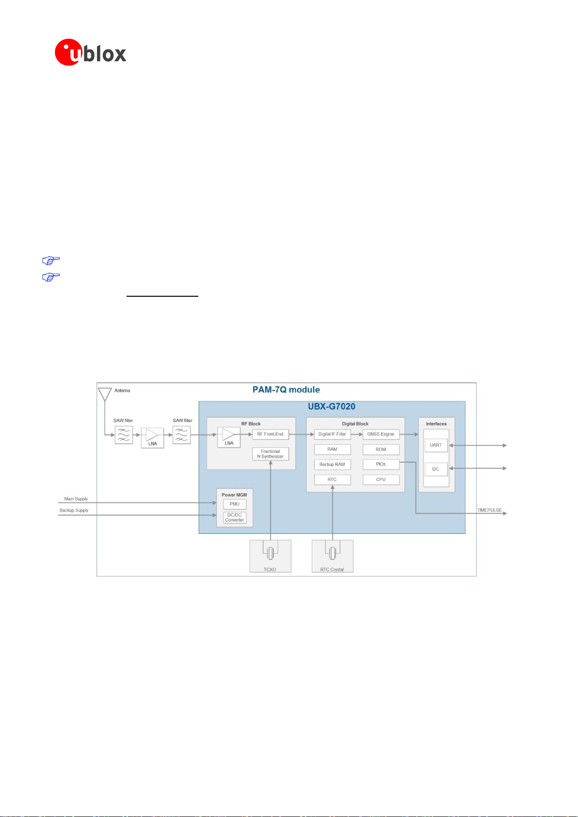
PAM-7Q module consists of two functional parts - the RF block and the digital block (see Figure 1).
The RF block includes the input matching elements, the SAW band pass filter, the integrated LNA and the
oscillator, while the digital block contains the u-blox 7 GNSS engine, the RTC crystal and additional elements
such as the optional FLASH Memory for enhanced programmability and flexibility.
Figure 1: PAM-7Q block diagram
2.3 Operating modes
u-blox receivers support different power modes. These modes represent strategies of how to control the
acquisition and tracking engines in order to achieve either the best possible performance or good performance
with reduced power consumption.
2.3.1 Continuous Mode
During a cold start, a receiver in Continuous Mode continuously deploys the acquisition engine to search for all
satellites. Once the receiver can calculate a position and track a sufficient number of satellites, the acquisition
engine powers off, resulting in significant power savings. The tracking engine continuously tracks acquired
UBX-13003143 - R06 Early Production Information Quick reference
Page 6 of 26
Page 7

PAM-7Q - Hardware Integration Manual
Baud Rate
String
UART Baud Rate 1200
B5 62 06 41 09 00 01 01 30 81 00 00 00 00 FE 01 22
UART Baud Rate 2400
B5 62 06 41 09 00 01 01 30 81 00 00 00 00 FD 00 21
UART Baud Rate 4800
B5 62 06 41 09 00 01 01 30 81 00 00 00 00 FC FF 20
UART Baud Rate 19200
B5 62 06 41 09 00 01 01 30 81 00 00 00 00 FB FE 1F
UART Baud Rate 38400
B5 62 06 41 09 00 01 01 30 81 00 00 00 00 FA FD 1E
UART Baud Rate 57600
B5 62 06 41 09 00 01 01 30 81 00 00 00 00 F9 FC 1D
UART Baud Rate 115200
B5 62 06 41 09 00 01 01 30 81 00 00 00 00 F8 FB 1C
satellites and acquires other available or emerging satellites. Whenever the receiver can no longer calculate a
position or the number of satellites tracked is below the sufficient number, the acquisition engine powers on
again to guarantee a quick reacquisition. Even if the acquisition engine powers off, the tracking engine
continues to acquire satellites.
For best performance, use continuous mode.
2.3.2 Power Save Mode
Two Power Save Mode (PSM) operations called ON/OFF and Cyclic tracking are available. These use different
ways to reduce the average current consumption in order to match the needs of the specific application. PSM
operations are set and configured using serial commands. For more information, see the u-blox 7 Receiver
Description Including Protocol Specification [2].
2.4 Configuration
The configuration settings can be modified using UBX protocol configuration messages. The modified settings
remain effective until power-down or reset. If these settings have been stored in BBR (Battery Backed RAM), then
the modified configuration will be retained, as long as the backup battery supply is not interrupted.
.
2.4.1 Electrical Programmable Fuse (eFuse)
PAM-7Q includes an integrated eFuse memory for permanently saving configuration settings.
The eFuse memory can also be used to store the configuration. The customer can program the eFuse.
eFuse is One-Time-Programmable; it cannot be changed if it has been programmed once.
String to change the default Baud rate:
Table 1: Strings to change baud rate
2.5 Connecting power
The PAM-7Q positioning module has two power supply pins: VCC and V_BCKP.
2.5.1 VCC: Main Supply Voltage
The VCC pin provides the main supply voltage. During operation, the current drawn by the module can vary by
some orders of magnitude, especially if enabling low-power operation modes. For this reason, it is important
that the supply circuitry be able to support the peak power (see datasheet for specification) for a short time.
PAM-7Q module integrates a DC/DC converter. This allows reduced power consumption, especially when using
a main supply voltage above 2.5 V.
UBX-13003143 - R06 Early Production Information Hardware description
Page 7 of 26
Page 8
PAM-7Q - Hardware Integration Manual
When switching from backup mode to normal operation or at start-up, PAM-7Q module must charge
the internal capacitors in the core domain. In certain situations, this can result in a significant current
draw. For low power applications using Power Save and backup modes, it is important that the power
supply or low ESR capacitors at the module input can deliver this current.
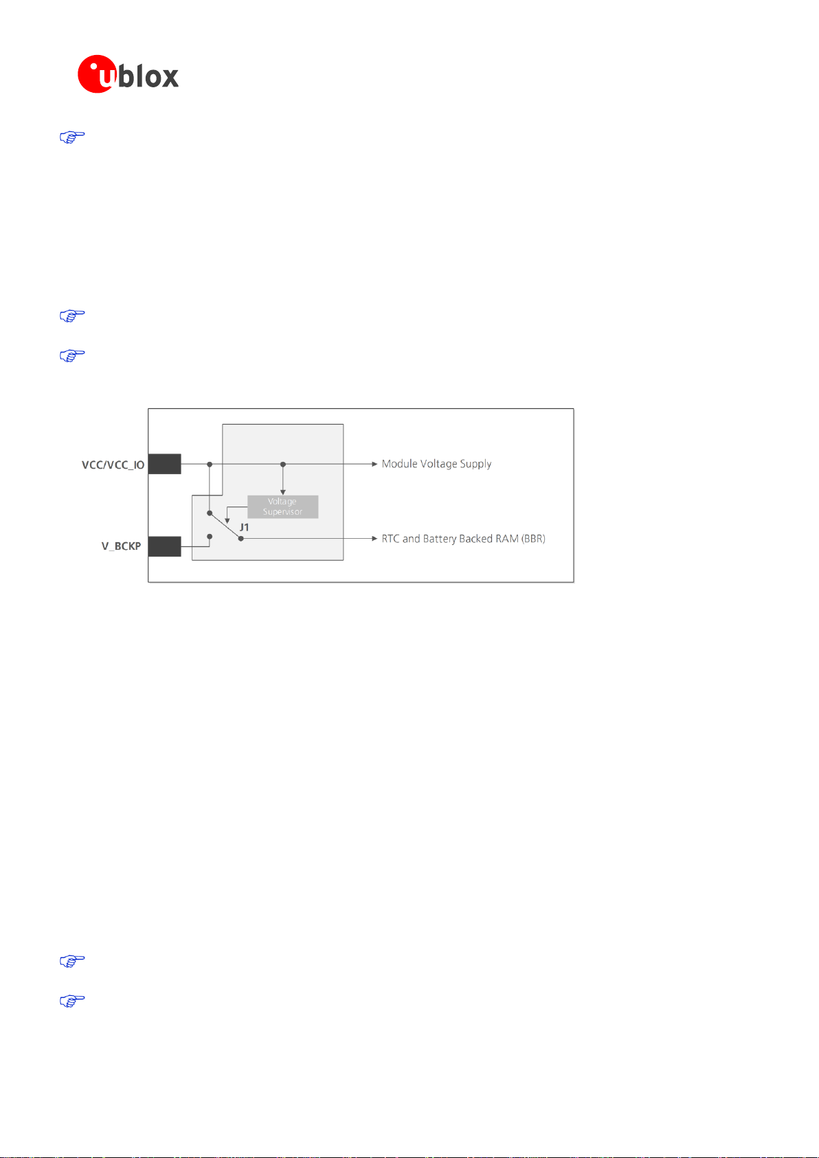
2.5.2 V_BCKP: Backup Supply Voltage
If the module supply has a power failure, then V_BCKP will supply the real-time clock (RTC) and battery backed
RAM (BBR). Use of valid time and the GNSS orbit data at start-up will improve the GNSS performance, as with
hot starts, warm starts, AssistNow Autonomous and AssistNow Offline. If no backup battery is connected, the
module performs a cold start at power up.
Avoid high resistance on the V_BCKP line: During the switch from main supply to backup supply, a short
current adjustment peak can cause high voltage drop on the pin with possible malfunctions.
As long as the PAM-7Q module is supplied to VCC, the backup battery is disconnected from the RTC
and the BBR to avoid unnecessary battery drain (see Figure 2). In this case, VCC supplies power to the
RTC and BBR.
Figure 2: Backup battery and voltage (for exact pin orientation, see data sheet)
2.6 Interfaces
2.6.1 UART
PAM-7Q positioning module includes a Universal Asynchronous Receiver Transmitter (UART) serial interface
RxD/TxD supporting configurable baud rates. The baud rates supported are specified in the u-blox 7 Receiver
Description Including Protocol Specification [2].
The signal output and input levels are 0 V to VCC. An interface based on RS232 standard levels (+/- 12 V) can be
implemented using level shifters such as Maxim MAX3232. Hardware handshake signals and synchronous
operation are not supported.
2.6.2 Display Data Channel (DDC)
An I2C compatible Display Data Channel (DDC) interface is available for serial communication with an external
host CPU. The interface only supports operation in slave mode (master mode is not supported). The DDC
protocol and electrical interface are fully compatible with the Fast-Mode of the I2C industry standard. DDC pins
SDA and SCL have internal pull-up resistors.
For more information about the DDC implementation, see the u-blox 7 Receiver Description Including Protocol
Specification [2]. For bandwidth information, see the Data Sheet. For timing, parameters consult the I 2C-bus
specification [7].
The u-blox 7 DDC interface supports serial communication with u-blox cellular modules. See the
specification of the applicable cellular module to confirm compatibility.
With u-blox 7, when reading the DDC internal register at address 0xFF (messages transmit buffer), the
master must not set the reading address before every byte is accessed, as this could cause faulty behavior.
UBX-13003143 - R06 Early Production Information Hardware description
Page 8 of 26
Page 9

PAM-7Q - Hardware Integration Manual
After every byte is read from register 0xFF, the internal address counter is incremented by one, saturating
at 0xFF. Therefore, subsequent reads can be performed continuously.
2.7 I/O pins
2.7.1 TIMEPULSE
A configurable time pulse signal is available with the PAM-7Q module. By default, the time pulse signal is
configured to 1 pulse per second. For more information see the u-blox 7 Receiver Description including Protocol
Specification [2].
UBX-13003143 - R06 Early Production Information Hardware description
Page 9 of 26
Page 10

PAM-7Q - Hardware Integration Manual
3 Design
3.1 Design checklist
Designing-in a PAM-7Q module is easy, especially when based on a u-blox reference design. This section lists the
most important items for a simple design check. The design checklist can also help to avoid an unnecessary PCB
respin and achieve the best possible performance. Follow the design checklists when developing PAM-7Q GPS
applications. This can significantly reduce development time and costs.
3.1.1 Schematic checklist
Power supply requirements
GNSS positioning modules require a stable power supply. In selecting a strategy to achieve a clean and
stable power supply, any resistance in the VCC supply line can negatively influence performance.
Consider the following points:
o Wide power lines or even power planes are preferred.
o Avoid resistive components in the power line (e.g. narrow power lines, coils, resistors, etc.).
o Placing a filter or other source of resistance at VCC can create significantly longer acquisition
times.
Is the power supply (VCC) within the specified range? (see the PAM-7Q Data Sheet [1])
Compare the peak supply current consumption of your PAM-7Q module with the specification of the
power supply. (See the PAM-7Q Data Sheet [1] for more information.)
At the module input, use low ESR capacitors that can deliver the required current/charge for switching
from backup mode to normal operation.
Backup battery
Use of valid time and the GNSS orbit data at startup will improve the GNSS performance i.e. enables hot
starts, warm starts and the AssistNow Autonomous process as well as AssistNow Offline. To make use of
these features connect a battery to V_BCKP to continue supplying the backup domain in case of power
failure at VCC.
If no backup supply voltage is available, connect the V_BCKP pin to VCC).
UBX-13003143 - R06 Early Production Information Design
Page 10 of 26
Page 11

PAM-7Q - Hardware Integration Manual
3.1.2 Layout checklist
See section 3.3.
Is the GNSS module located according to the recommendation?
Has the grounding concept been followed?
Add a ground plane underneath the GNSS module to reduce interference.
For improved shielding, add as many vias as possible around the serial communication lines, underneath
the GNSS module etc.
Have appropriate EOS/ESD/EMI protection measures been included? This is especially important for
designs including cellular modules.
3.1.3 Antenna checklist
Make sure the antenna is not placed close to noisy parts of the circuitry. (E.g. micro-controller, display,
etc.)
3.2 Design considerations for minimal designs
For a minimal design with a PAM-7Q GPS module, the following functions and pins need consideration:
Connect the Power supply to VCC.
Assure an optimal ground connection to all ground pins of the module.
Choose the required serial communication interface (UART or DDC) and connect the appropriate pins to
your application.
If you need improved start-up or use AssistNow Autonomous in your application, connect a backup supply
voltage to V_BCKP.
3.2.1 Minimal design
This is a minimal setup for a GNSS receiver with a PAM-7Q module:
Figure 3: PAM-7Q passive antenna design
UBX-13003143 - R06 Early Production Information Design
Page 11 of 26
Page 12

PAM-7Q - Hardware Integration Manual
Function
PIN
No
I/O
Description
Remarks
Power
VCC 4 I
Supply Voltage
Provide clean and stable supply.
GND 3 I
Ground
Assure a good GND connection to GND pin of the module,
preferably with a large ground plane.
V_BCKP
5 I Backup Supply
Voltage
It is recommended to connect a backup supply voltage to V_BCKP
in order to enable warm and hot start features on the positioning
modules. Otherwise, connect to VCC.
UART
TxD
2 O Serial Port
Communication interface
RxD 1 I
Serial
Serial input. Internal pull-up resistor to VCC. Leave open if not used.
System
TIMEPULSE
6 O Time pulse
Signal
Configurable Time pulse signal (one pulse per second by default).
Leave open if not used.
SDA 7 I/O
DDC Data
DDC Data
SCL 8 I
DDC Clock
DDC Clock.
Table 2: Pinout PAM-7Q
3.3 Layout
This section provides important information for designing a robust GNSS system.
GNSS signals at the surface of the Earth are about 15 dB below the thermal noise floor. When defining a GNSS
receiver layout, the placement of the PAM-7Q, as well as grounding, shielding and jamming from other digital
devices, are crucial issues requiring careful consideration.
3.3.1 PCB mounting
The PAM-7Q can be mounted on a customer PCB (“motherboard” in the instructions below) by using standard
2.54 mm pitch 1x8 pin header (for example Samtec TLW-108-06-G-S). Two dummy pads are used to solder the
module metal shield on the motherboard. Reference pad layout is shown in Figure 4.
UBX-13003143 - R06 Early Production Information Design
Page 12 of 26
Page 13

PAM-7Q - Hardware Integration Manual
Figure 4: Pad layout of mounting side for PAM-7Q module.
There are some rules that need to be followed in order to maintain good performance for the on-board patch
antenna of the PAM-7Q:
Solder the pin header to the module in such way that the pins are as short as possible on the antenna
side of the PAM-7Q module (see Figure 5).
Place any active circuitry (processors, memory busses, switching regulators, etc.) on the motherboard as
far away as possible from the PAM-7Q module.
Design a solid VDD source for the PAM-7Q module (VDD supply voltage ripple should be <50 mVp-p).
If there is no need for the PPS and DDC signal, a 4-pin header (for example Samtec TLW-104-06-G-S)
can be used to contact pins #1 through #4. However, the 8-pin header is recommended since it is
mechanically more robust. In this case, pins #5 to #8 may be left floating on the motherboard.
Figure 5: Side view of the pin header assembly for the PAM-7Q module.
Figure 6 describes the footprint for PAM-7Q module.
UBX-13003143 - R06 Early Production Information Design
Page 13 of 26
Page 14

PAM-7Q - Hardware Integration Manual
Figure 6: PAM-7Q footprint
3.3.2 Placement
A very important factor in achieving maximum performance is the placement of the receiver on the PCB. Make
sure that the PAM-7Q is separated from any other digital circuits on the system board. To achieve this, position
the module’s digital part towards the digital section on the system PCB. Exercise care if placing the receiver in
proximity to heat-emitting circuitry. The RF part of the receiver is very sensitive to temperature, and sudden
changes can have an adverse impact on performance.
The RF part of the receiver is a temperature sensitive component. Avoid high temperature
drift and air vents near the receiver.
UBX-13003143 - R06 Early Production Information Design
Page 14 of 26
Page 15

4 Migration to PAM-7Q module
Pin
Fastrax UP501
PAM-7Q
1
RXD
RxD 2 TXD
TxD 3 GND
GND 4 VDD 3.0 to 4.2 V
VCC 2.7 to 3.6 V
5
VDD_B 2.0 to 4.2 V
V_BCKP 1.4 to 3.6 V
6
PPS
TIMEPULSE
7 - SDA
8 - SCL
4.1 Hardware migration
The PAM-7Q is form-factor compatible with the UP501.
Table 3: Pins for UP501 to PAM-7Q migration
PAM-7Q - Hardware Integration Manual
4.2 Software migration
Fastrax UP501 is based on MTK chipset, while PAM-7Q has u-blox 7 GNSS engine. For functionality aspects,
protocol porting, and software interface considerations when migrating from the Fastrax UP501 to the u-blox
PAM-7Q, see the NMEA manual for Fastrax IT500 Series GPS/GNSS receivers [6] and the u-blox 7 Receiver
Description including Protocol Specification [2].
UBX-13003143 - R06 Early Production Information Migration to PAM-7Q module
Page 15 of 26
Page 16

PAM-7Q - Hardware Integration Manual
5 Product handling
5.1 Packaging, shipping and storage
For information pertaining to reels and tapes, shipment and storage information, as well as drying for
preconditioning, see the specific PAM-7Q Data Sheet [1].
5.2 Soldering
5.2.1 Hand soldering
Use a soldering iron temperature setting equivalent to 350 °C.
5.2.2 Optical inspection
After soldering the PAM-7Q module, consider an optical inspection step to check whether:
The module is properly aligned
All pads are properly soldered
No excess solder has created contacts to neighboring pads, or possibly to pad stacks and vias nearby
5.2.3 Cleaning
In general, cleaning the populated modules is strongly discouraged. Residues underneath the modules cannot be
easily removed with a washing process.
Cleaning with water will lead to capillary effects where water is absorbed in the gap between the baseboard
and the module. The combination of residues of soldering flux and encapsulated water leads to short circuits
or resistor-like interconnections between neighboring pads.
Cleaning with alcohol or other organic solvents can result in soldering flux residues flooding into the two
housings, areas that are not accessible for post-wash inspections. The solvent will also damage the sticker
and the ink-jet printed text.
Ultrasonic cleaning will permanently damage the module, in particular the quartz oscillators.
The best approach is to use a "no clean" soldering paste and eliminate the cleaning step after the soldering.
5.2.4 Rework
The PAM-7Q module can be unsoldered from the baseboard using a hot air gun or a soldering iron. Use a wide
iron tip to unsolder all the pins at the same time. In general, we do not recommend using a hot air gun because
this is an uncontrolled process and might damage the module.
Attention: use of a hot air gun can lead to overheating and severely damage the module.
Always avoid overheating the module.
After the module is removed, clean the pads before placing and hand soldering a new module.
Never attempt a rework on the module itself, e.g. replacing individual components. Such
actions immediately terminate the warranty.
In addition, manual rework on particular pins by using a soldering iron is allowed. Manual rework steps on the
module can be done several times.
5.2.5 Conformal coating
Certain applications employ a conformal coating of the PCB using HumiSeal® or other related coating products.
These materials affect the HF properties of the GNSS module, and it is important to prevent them from flowing
into the module. The RF shields do not provide 100% protection for the module from coating liquids with low
viscosity; therefore, care is required in applying the coating.
UBX-13003143 - R06 Early Production Information Product handling
Page 16 of 26
Page 17

PAM-7Q - Hardware Integration Manual
Conformal Coating of the module will void the warranty.
5.2.6 Casting
Casting is not allowed. The OEM is strongly advised to qualify such processes in combination with the PAM-7Q
module before implementing this in the production.
Antenna element of PAM-7Q must have free space at least 1mm for any plastic case or radome.
5.2.7 Grounding metal covers
Attempts to improve grounding by soldering ground cables, wick or other forms of metal strips directly onto the
EMI covers is done at the customer's own risk. The numerous ground pins should be sufficient to provide
optimum immunity to interferences and noise.
u-blox makes no warranty for damages to the PAM-7Q module caused by soldering metal cables or any
other forms of metal strips directly onto the EMI covers.
5.2.8 Use of ultrasonic processes
Some components on the PAM-7Q module are sensitive to Ultrasonic Waves. Use of any Ultrasonic Processes
(cleaning, welding etc.) may cause damage to the GNSS Receiver.
u-blox offers no warranty against damages to the PAM-7Q module caused by any Ultrasonic Processes.
5.3 EOS/ESD/EMI precautions
When integrating GNSS positioning modules into wireless systems, careful consideration must be given to
electromagnetic and voltage susceptibility issues. Wireless systems include components, which can produce
Electrical Overstress (EOS) and Electro-Magnetic Interference (EMI). CMOS devices are more sensitive to such
influences because their failure mechanism is defined by the applied voltage, whereas bipolar semiconductors
are more susceptible to thermal overstress. The following design guidelines are provided to help in designing
robust yet cost effective solutions.
To avoid overstress damage during production or in the field it is essential to observe strict
EOS/ESD/EMI handling and protection measures.
To prevent overstress damage at the RF_IN of your receiver, never exceed the maximum input
power (see the PAM-7Q Data Sheet [1]).
5.3.1 Electrostatic discharge (ESD)
Electrostatic discharge (ESD) is the sudden and momentary electric current that flows between
two objects at different electrical potentials caused by direct contact or induced by an
electrostatic field. The term is usually used in the electronics and other industries to describe
momentary unwanted currents that may cause damage to electronic equipment.
5.3.2 ESD handling precautions
ESD prevention is based on establishing an Electrostatic Protective Area (EPA). The EPA can be a small working
station or a large manufacturing area. The main principle of an EPA is that there are no highly charging materials
near ESD sensitive electronics, all conductive materials are grounded, workers are grounded, and charge build-up
on ESD sensitive electronics is prevented. International standards are used to define typical EPA and can be
obtained for example from International Electrotechnical Commission (IEC) or American National Standards
Institute (ANSI).
GNSS positioning modules are sensitive to ESD and require special precautions when handling. Particular care
must be exercised when handling patch antennas, due to the risk of electrostatic charges. In addition to
standard ESD safety practices, the following measures should be taken into account whenever handling the
receiver.
UBX-13003143 - R06 Early Production Information Product handling
Page 17 of 26
Page 18

PAM-7Q - Hardware Integration Manual
Unless there is a galvanic coupling between the local GND (i.e. the
work table) and the PCB GND, then the first point of contact when
handling the PCB must always be between the local GND and PCB
GND.
Before mounting an antenna patch, connect ground of the device
When handling the RF pin, do not come into contact with any
charged capacitors and be careful when contacting materials that
can develop charges (e.g. patch antenna ~10 pF, coax cable ~50 80 pF/m, soldering iron, …)
To prevent electrostatic discharge through the RF input, do not
touch any exposed antenna area. If there is any risk that such
exposed antenna area is touched in non ESD protected work area,
implement proper ESD protection measures in the design.
When soldering RF connectors and patch antennas to the receiver’s
RF pin, make sure to use an ESD safe soldering iron (tip).
Failure to observe these precautions can result in severe damage to the GNSS module!
5.3.3 ESD protection measures
GNSS positioning modules are sensitive to Electrostatic Discharge (ESD). Special precautions
are required when handling.
5.3.4 Electromagnetic interference (EMI)
Electromagnetic interference (EMI) is the addition or coupling of energy originating from any RF emitting device.
This can cause a spontaneous reset of the GNSS receiver or result in unstable performance. Any unshielded line
or segment (>3mm) connected to the GNSS receiver can effectively act as antenna and lead to EMI disturbances
or damage.
The following elements are critical regarding EMI:
Unshielded connectors (e.g. pin rows etc.)
Weakly shielded lines on PCB (e.g. on top or bottom layer and especially at the border of a PCB)
Weak GND concept (e.g. small and/or long ground line connections)
EMI protection measures are recommended when RF emitting devices are near the GNSS receiver. To minimize
the effect of EMI a robust grounding concept is essential. To achieve electromagnetic robustness follow the
standard EMI suppression techniques.
http://www.murata.com/products/emc/knowhow/index.html
http://www.murata.com/products/emc/knowhow/pdf/4to5e.pdf
Improved EMI protection can be achieved by inserting a resistor (e.g. R>20 ) or better yet a ferrite bead
(BLM15HD102SN1) or an inductor (LQG15HS47NJ02) into any unshielded PCB lines connected to the GNSS
receiver. Place the resistor as close as possible to the GNSS receiver pin.
UBX-13003143 - R06 Early Production Information Product handling
Page 18 of 26
Page 19
PAM-7Q - Hardware Integration Manual
TX
RX
GPS
Receiver
FB
FB
BLM15HD102SN1
>10mm
1525 1550 1625
GPS input filter
characteristics
1575 1600
0
-110
Jammin
g signal
1525 1550 1625
Frequency [MHz]
Power [dBm]
GPS input filter
characteristics
1575 1600
0
Jamming
signal
GPS
signals
GPS Carrier
1575.4 MHz
Example of EMI protection measures on the RX/TX line using a ferrite bead:
Figure 7: EMI Precautions
VCC can be protected using a feed thru capacitor.
Intended use
In order to mitigate any performance degradation of a radio equipment under EMC disturbance, system
integration shall adopt appropriate EMC design practice and not contain cables over three meters on
signal and supply ports.
5.3.5 Applications with cellular modules
GSM uses power levels up to 2 W (+33 dBm). Consult the Data Sheet for the absolute maximum power input at
the GNSS receiver.
5.3.5.1 Isolation between GPS and GSM antenna
In a handheld type design, an isolation of approximately 20 dB can be reached with careful placement of the
antennas relative to the GPS receiver.
5.3.5.2 Increasing jamming immunity
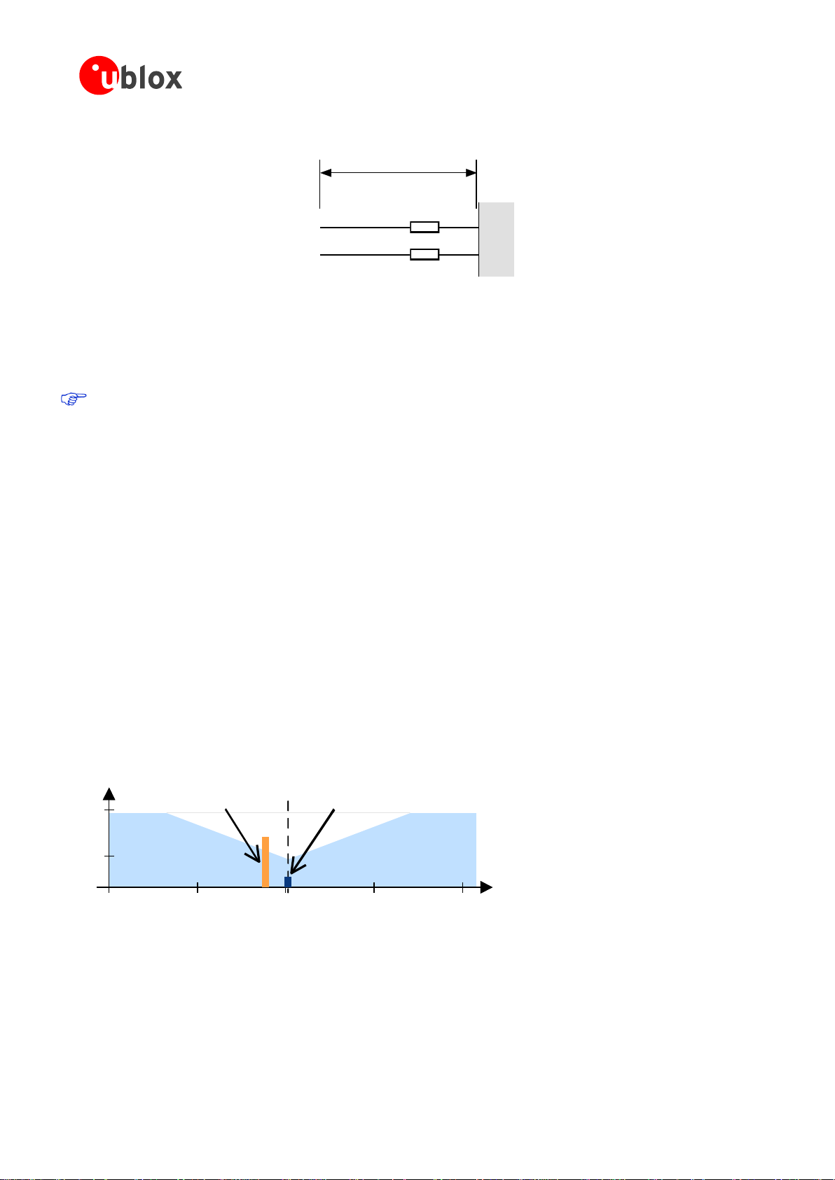
Jamming signals come from in-band and out-band frequency sources.
5.3.5.3 In-band jamming
With in-band jamming the signal frequency is very close to the GPS frequency of 1575 MHz (see Figure 8). Such
jamming signals are typically caused by harmonics from displays, micro-controller, bus systems, etc.
Figure 8: In-band jamming signals
UBX-13003143 - R06 Early Production Information Product handling
Page 19 of 26
Page 20

PAM-7Q - Hardware Integration Manual
Figure 9: In-band jamming sources
Measures against in-band jamming include:
Maintaining a good grounding concept in the design
Shielding
Layout optimization
Filtering
Placement of the GPS antenna
5.3.5.4 Out-band jamming
Out-band jamming is caused by signal frequencies that are different from the GPS carrier (see Figure 10). The
main sources are wireless communication systems such as GSM, CDMA, WCDMA, Wi-Fi, BT, etc.
Figure 10: Out-band jamming signals
Measures against out-band jamming include maintaining a good grounding concept in the design.
For design-in recommendations in combination to Cellular operation see Appendix (Appendix A.1).
See the GPS Implementation and Aiding Features in u-blox wireless modules [5].
UBX-13003143 - R06 Early Production Information Product handling
Page 20 of 26
Page 21

PAM-7Q - Hardware Integration Manual
Figure 11: Automatic Test Equipment for Module Tests
Figure 12: X-Ray Inspection
6 Product testing
6.1 u-blox in-series production test
u-blox focuses on high quality for its products. To achieve a high standard it is our philosophy to supply fully
tested units. Therefore, at the end of the production process, every unit is tested. Defective units are analyzed in
detail to improve the production quality.
This is achieved with automatic test equipment, which delivers a detailed test report for each unit. The following
measurements are done:
Digital self-test (Software Download, verification of FLASH firmware, etc.)
Measurement of voltages and currents
Measurement of RF characteristics (e.g. C/No)
Traceability down to component level
X-Ray and Automated Optical Inspection (AOI)
Ongoing Reliability Tests
6.2 Test parameters for OEM manufacturer
Because of the testing done by u-blox (with 100% coverage), it is obvious that an OEM manufacturer does not
need to repeat firmware tests or measurements of the GNSS parameters/characteristics (e.g. TTFF) in their
production test.
An OEM manufacturer should focus on:
Overall sensitivity of the device (including antenna, if applicable)
Communication to a host controller
UBX-13003143 - R06 Early Production Information Product testing
Page 21 of 26
Page 22

PAM-7Q - Hardware Integration Manual
6.3 System sensitivity test
The best way to test the sensitivity of a GNSS device is with the use of a 1-channel GNSS simulator. It assures
reliable and constant signals at every measurement.
Figure 13: 1-channel GNSS simulator
u-blox recommends the following Single-Channel GNSS Simulator:
Spirent GSS6100 (GPS)
Spirent GSS6300 (GPS/GLONASS)
Spirent Communications Positioning Technology www.spirent.com
6.3.1 Guidelines for sensitivity tests
1. Connect a 1-channel GNSS simulator to the OEM product via an antenna.
2. Choose the power level in a way that the “Golden Device” would report a C/No ratio of 38-40 dBHz
3. Power up the DUT (Device Under Test) and allow enough time for the acquisition
4. Read the C/No value from the NMEA GSV or the UBX-NAV-SVINFO message (e.g. with u-center)
5. Compare the results to a “Golden Device” or a PAM-7Q Evaluation Kit.
6.3.2 ‘Go/No go’ tests for integrated devices
The best test is to bring the device to an outdoor position with excellent sky view (HDOP < 3.0). Let the
receiver acquire satellites and compare the signal strength with a “Golden Device”.
As the electro-magnetic field of a redistribution antenna is not homogenous, indoor tests are in most
cases not reliable. These kind of tests may be useful as a ‘go/no go’ test but not for sensitivity
measurements.
UBX-13003143 - R06 Early Production Information Product testing
Page 22 of 26
Page 23

Appendix
Abbreviation
Definition
ANSI
American National Standards Institute
CDMA
Code Division Multiple Access
EMC
Electromagnetic compatibility
EMI
Electromagnetic interference
EOS
Electrical Overstress
EPA
Electrostatic Protective Area
ESD
Electrostatic discharge
GLONASS
Russian satellite system
GND
Ground
GNSS
Global Navigation Satellite System (general term for any system, GPS, GLONASS, etc.)
GPS
Global Positioning System
GSM
Global System for Mobile Communications
IEC
International Electrotechnical Commission
PCB
Printed circuit board
QZSS
Quasi-Zenith Satellite System
A Abbreviations
PAM-7Q - Hardware Integration Manual
Table 4: Explanation of abbreviations used
UBX-13003143 - R06 Early Production Information Appendix
Page 23 of 26
Page 24

PAM-7Q - Hardware Integration Manual
Product Receiver Chain
Cellular and GNSS
Simultaneous operation
Family
Variant
Antenna
SAW LNA On-chip LNA
SAW
Passive GNSS
Antenna
Active GNSS
Antenna
SAW
2G cellular
3G/4G cellular
2G/3G/4G
cellular
MAX-6
Any
•
•
NEO-6
Any
•
•
LEA-6
Any
•
•
EVA-7
M
•
MAX-7
C
•
W
•
Q
•
NEO-7
N
•
•
M
•
P
•
•
PAM-7
Q
•
•
•
•
A.1 Design-in recommendations in combination with cellular operation
• = integrated = optimal performance
Table 5: Combinations of u-blox GNSS modules with different cellular technologies (2G/3G/4G).
See the GPS Implementation and Aiding Features in u-blox wireless modules [5].
UBX-13003143 - R06 Early Production Information Appendix
Page 24 of 26
Page 25

PAM-7Q - Hardware Integration Manual
Revision
Date
Name
Status / Comments
R01
07-Nov-2013
jfur
Objective Specification
R02
23-Jan-2014
jfur
Advance Information. Updated product picture (patch antenna side) in cover page.
Updated section 5.2 Soldering.
R03
05-Mar-2014
jfur
Early Production Information
R04
12-May-2014
jfur
Added • = integrated
= optimal performance
Table 5: Blocking dependence on different cellular technology (2G/3G/4G).
R05
05-Dec-2014
jfur
Removed section wave soldering and ground plane related contents.
R06
06-Oct-2017
msul
Added information on RED DoC in European Union regulatory compliance (page 2), added
Intended use statement in section 5.3.4 Electromagnetic interference (EMI), updated legal
statement in cover page and added Documentation feedback e-mail address in contacts
page.
Related documents
[1] PAM-7Q Data Sheet, Docu. No UBX-13002455
[2] u-blox 7 Receiver Description including Protocol Specification, Docu. No GPS.G7-SW-12001
[3] u-blox 7 Firmware Version 1.0 Release Note, Docu. No GPS.G7-SW-12003
[4] GPS Compendium, Doc No GPS-X-02007
[5] GPS Implementation and Aiding Features in u-blox wireless modules, Doc No GSM.G1-CS-09007
[6] NMEA manual for Fastrax IT500 Series GPS/GNSS receivers, Docu. No UBX-13003181
[7] I
2
C-bus specification, Rev. 5, Oct 2012, http://www.nxp.com/documents/other/UM10204_v5.pdf
For regular updates to u-blox documentation and to receive product change notifications please register
on our homepage (http://www.u-blox.com)
Revision history
UBX-13003143 - R06 Early Production Information Appendix
Page 25 of 26
Page 26

Contact
u-blox Offices
North, Central and South America
u-blox America, Inc.
Phone: +1 703 483 3180
E-mail: info_us@u-blox.com
Regional Office West Coast:
Phone: +1 408 573 3640
E-mail: info_us@u-blox.com
Technical Support:
Phone: +1 703 483 3185
E-mail: support_us@u-blox.com
Headquarters
Europe, Middle East, Africa
u-blox AG
Phone: +41 44 722 74 44
E-mail: info@u-blox.com
Support: support@u-blox.com
Documentation Feedback
E-mail: docsupport@u-blox.com
Asia, Australia, Pacific
u-blox Singapore Pte. Ltd.
Phone: +65 6734 3811
E-mail: info_ap@u-blox.com
Support: support_ap@u-blox.com
Regional Office Australia:
Phone: +61 2 8448 2016
E-mail: info_anz@u-blox.com
Support: support_ap@u-blox.com
Regional Office China (Beijing):
Phone: +86 10 68 133 545
E-mail: info_cn@u-blox.com
Support: support_cn@u-blox.com
Regional Office China (Chongqing):
Phone: +86 23 6815 1588
E-mail: info_cn@u-blox.com
Support: support_cn@u-blox.com
Regional Office China (Shanghai):
Phone: +86 21 6090 4832
E-mail: info_cn@u-blox.com
Support: support_cn@u-blox.com
Regional Office China (Shenzhen):
Phone: +86 755 8627 1083
E-mail: info_cn@u-blox.com
Support: support_cn@u-blox.com
Regional Office India:
Phone: +91 80 4050 9200
E-mail: info_in@u-blox.com
Support: support_in@u-blox.com
Regional Office Japan (Osaka):
Phone: +81 6 6941 3660
E-mail: info_jp@u-blox.com
Support: support_jp@u-blox.com
Regional Office Japan (Tokyo):
Phone: +81 3 5775 3850
E-mail: info_jp@u-blox.com
Support: support_jp@u-blox.com
Regional Office Korea:
Phone: +82 2 542 0861
E-mail: info_kr@u-blox.com
Support: support_kr@u-blox.com
Regional Office Taiwan:
Phone: +886 2 2657 1090
E-mail: info_tw@u-blox.com
Support: support_tw@u-blox.com
For complete contact information, visit us at www.u-blox.com
PAM-7Q - Hardware Integration Manual
UBX-13003143 - R06 Early Production Information Contact
Page 26 of 26
 Loading...